Note: Descriptions are shown in the official language in which they were submitted.
i;~97590
20104-7753
Data processing device composed of four data processing modules of
substantially identical construction, with protection both against
simultaneous single-bit failures in a plurality of data processing
modules and against failure of a single data processing module.
BACKGROUND TO THE INVENTION
The invention relates to a data processing device which
is composed of four processing modules of substantially identical
construction, with protection both against coincident single-bit
failures in a plurality of data processing modules and also
against an arbitrary data failure in a single data processing
module. A device of this kind is known from US patent 4512020
(PHN 10155) of applicant. The known device operates on the basis
of so-called symbols of four bits, while an optimum code as
therein presented allows in a so-called 'normal mode' for
correcting of two arbitrary single bit errors, at a minimum
Hamming distance of five. In an 'erasure' mode, one of the data
processlng modules is ignored while the code over the remaining
three four-bit symbols has a Hamming distance of three, allowing
for one additional bit-error to be correctable. If any two data
processing modules would fail simultaneously while their identity
is known, the two remaining data processing modules, in the
absence of further errors, could still function and attain the
correct results. The above error protection capability may be
expressed in the minimum distance profile of this code at a
redundancy of 100% as being (5,3,1). The definition of minimum
~297590
20104-7753
distance profile is given hereinafter.
SUMMARY OF THE INVENTION
Data processing technology has evolved to processors
having an increased bit width. It is an object of the invention
of improving the aforesaid error protection capability at the same
amount of redundancy by using 8-bit symbols to optimally realize a
minimum distance profile of (7,4,1). That is, in the normal mode
the distance is 7, allowing for the correction of three arbitrary
single bit errors. It is known in the art, that this degree of
protection may also be used to correct up to two arbitrary single
bit errors and to detect up to four arbitrary single bit errors.
Other trade-offs between correction and detection are well known.
In the erasure mode, the minimum Hamming distance oE four allows
for single-bit correction, double-bit error detection, or
alternatively for triple-bit-error detection. Ignorin~ any
combination of two data processing modules in the absence of any
further error still allows the two remaining data processing
modules to attain correct results.
~`he object oE the invention is realized by a data
processing device comprising: (a) four data processing modules
which each include (i) corresponding data processing means having
a data path width of at least 2n bytes, where n is an integer
greater than or equal to one, (ii) a respective encoder module fed
by the corresponding data processing means for bytewise encoding a
processing result of 2n bytes to a respective encoding result of n
bytes, (iii) a respective memory module fed by the respective
12!~7S90
20104-7753
encoder module Eor storing the respective encoding result, P2(iv)
respective input decoders for receiving said encoding resul-ts in
groups of four bytes and therefrom reconstituting a two-byte data
word representing said processing result for presentation to the
corresponding data processing means, (b) an interconnection
network fed by the respective data processing modules for applying
encoding results between all data processing modules and the
respective input decoders, (c) mode register means for controlling
said input decoders so that they assume respective ~Eirst, second
and third modes, so that (i) in the first mode, said input
decoders accept and digest all bytes of one of said groups, (li)
in the second mode, the input decoders accept and digest three
bytes of one of said groups but reject an associated fourth byte
of said group, there being four possible modes designated the
second mode, and (iii) in the third mode, the input decoders
accept and digest two bytes of one of said groups but reject an
associated combination of two remaining bytes of said group, there
being six possible modes designated the third mode, and wherein
said encoder modules multiply each byte of a data word by a
regular matrix and add the multiplication bytes to produce a code
byte, the four code bytes thus generated by the respective encoder
modules constituting a code word, of a code with a minimum Hamming
distance over the bits of seven, the three code bytes accepted in
any second mode constituting a partial code word with a minimum
Hamming distance over the bits of four, the two bytes accepted in
any third mode constituting a representation of all bits of the
associated processing result.
2a
12g7~0
20104-7753
~RIEF DESCRIPTION O~ THE ~IGURES
The invention will be explained herein after with respect
to a preferred e-bodioent a~ exe~pli~ied by the following figures
Figure 1 gives a data proces~ing devices according to
the invention;
Figurc 2 give~ the parity chec~ ~atrices of nine code~
with re~pect to baset ~43 And egs having ~ini~u~ distance profile of t7,
4, 1);
Figure 3a, 3b, 3c give the binary ~epresentations of the
elc~ents of a particular Galoi~ field Gf (28);
Figure 3d i3 a so-called redundant parity check ~atrix;
Figure ~a gives A ~et of decoding definitions ;
Figure 4b gives a ~et of aessage esti ate~;
Figures 5a, 5b qive a li~t of all correctable error
cla~se3, their detection and ~e~age esti ate selection;
~igure 6 give~ the rule~ to the iaplenented by a
decoder;
Figure 7 qives a global decode de~ign
DESCR~PT~ON OF A PRE~ERRED EM~ODIHENT
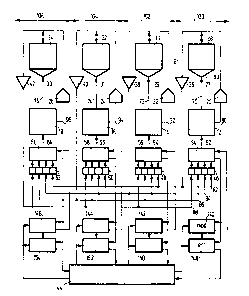
Fiqure 1 gives a data proces~ing device according to the
invention The data consist of wordJ, each word having sixteen bits and
repre~enting two Jynbol~ of a GaloiJ field to be explained hereina~ter
The data ~ords appear on the lines 62, 6~, 66, 68 They are
30 proce~sed in the re-~pective proces~or eleoents 12, 14, 16, 18 In
reaction thereto, the proce~sor ele-ent~ generate data re~ult~ words on
the line~ 90, 92, 94, g6 or address ~ords on the line~ 70, 72, 74, 76
A knswn ~eoory anage~ent unit (not ~hown) ~ay be pro~ided for each o~
the ~e~ory ~odules ~he local e~ories 28, 30, 32, 34 ~re atdre~ed
35 via the addres~ decoder~ 27, 29, 31, 33, Frou each 16-bit data word
recelved, an 8-bit code sy~bol i~ for~ed in each one of the code
generator3 20, 22, 24, 26, ~o that the code ~y~bol~ forned fro~ one
` 1;297S9~
PHN 11.853 4
data word together form one code word. ~hese code symbols are presented
to the memories 2B, 30, 32, 3q in order to be stored. The code symbols
after reading are regenerated in the read amplifiers 36, 38, 40, 42. The
regeneration can alternatively be realized without intermediate storage
in the memories~ The code symbols can all be applied to all registers
46, 48, 50, 52. These registers are connected to the reconstruction
devices or decoders 54, 56, 58, 60 for reconstructing the data words
from the code words for presentation to the lines 62, 64, 66. 68. The
combination of elements 46, 54, 12, 20, 28 and 36 is included in a
single separate error isolation zone and correspondingly for further
zones. It is assumed that the errors in two different zones are
independent; in many cases this re~uirement is satisfied for many
categories of errors if each error-isolation zone covers, for example,
a separate printed circuit board plus components, or alternatively a
separate integrated circuit. The circuit shown in the figure thus forms
four respective error isolation zones. The synchronization of the
operations in the four error isolation zones has been omitted for the
sake of clarity. The processors operate in accordance with programs. The
construction of the sub-systems in the relevant error-isolation zones is
identical, except for the code generators (20, 22, 24, 26) which each
implement a different algorithm for forming the four respective code
symbols from the 16-bit data word. Furthermore, the control of the data
reconstruction devices 54, 56, 58, 60 may differ depending on the
control mode of the computer system.It has been found that the normal
mode which is capable of correcting up to three arbitrarily situated bit
errors or a one-symbol error is very well suited for the correction of
errors occurring in the memory. These latter errors usually are mutually
independent and, moreover, are often so-called ~soft errors~. Symbol
erroxs which render an entire symbol unreliable are usually caused by a
faulty processor. These may be treated in an erasure mode wherein all
data and/or control signals produced by a selectable error isolation
zone or data processing module are ignored. It has been found that such
symbol errors are usually of a permanent nature. However, they need not
be repaired at short notice in this computer system, because the
decoders can switch over to the erasure mode. It has been found
advantageous to switch to the erasure mode as soon as necessary.
Furthermore, each error-isolation zone in Figure 1 comprises a separate
lZ97S90
20104-7753
error register (148,150,152,154) which is controlled by output
signals from the relevant decoder (54,56,58,60) and whose output
signals are applied to the central control device 44. Finally
there are shown reset lines for the error registers from the
central control unit 44. The multiplicity of these control lines
is not shown. Furthermore, each error-isolation zone comprises a
respective 4-bit mode register 140, 142, 144, 146. The mode
registers are controlied by output signals from the associated
decoders (54,56,58,60). The content of each mode register
controls the operating mode of the associated decoder. The
setting of the error register is co-controlled by the content of
the associated mode register. This relation is indicated each
time by an additional arrow. Finally, each mode register receives
control signals from the central control device 44. In another
realization, also the central control is distributed over the four
data processing modules. The communication system for
communicating control messages between those distributed control
modules (not shown) may be executed according to Canadian Patent
No. 1,241,758 of Applicant. The communication scheme allows for
arbitrary malfunction of one data processing module.
In the arrangement of Figure 1, in the error-free
condition, the same program is executed in all isolation zones.
This is also applicable in the normal mode. However, if a
systematic disturbance occurs in a given error isolation zone, the
symbol error having up to the bit weight 8 resulting therefrom, is
detected in the other isolation zones; these zones will switch
over to the erasure mode, so that the faulty isolation zone is no
~Z975~(~
20104-7753
longer taken into account. In the :Eaulty isolation zone itself
the signalling need not be correct; it may even occur that
completely different control occurs (for example, due to a failure
of the mode register). However, the system as a whole continues
to operate correctly thanks to the three other error isolation
zones.
CONSTRUCTION OF POSSIBLE CODES
In this section, the constructions of [4,2] codes over
the Galois field GF (28) having minimum distance profile (7,4,1)
are described.
5a
1297S9O
PHN 11.853 6
As alphabet we take GF t28) = 0,1,a,a2,....a254,
where a is a primitive root of the primitive polynominal x8+x4+x3
~x2+1 (for an extensive treatment of Galois fields, see F.J.
MacWilliams and D.J.A. Sloane, ~The Theory of Error-correcting Codes~,
North Holland Publ. Cy. Amsterdam 1977).
With respect to a basis < ab(0),ab(1),...,ab(7) ~
of GF (28) over GF (2), the elements of GF (28) can be represented
as binary vectors of length 8. For ~ ~GF(28),(aO,a1,..., a7) is
the binary representation of ~ if
= I ai ab(i)
i=O
A [~,2] code over GF (28) has a systematic parity- check matrix of the following form:
1 0 aP11 aP12
H =
I 0 1 aP21 aP22J
The problem is to find an 8-tuple (b(O),b(1),...,b(7))
and a 4-tuple (P11lp12lp21lp22) such that the [4,2] code
with parity check matrix H has a ~large~ minimum distance profile with
respect to the basis < ab(0),ab(1),....,ab(7)>. The minimum
distance profile of any t4,2] code over GF (28) can be proven to have
no higher elements than those of the profile (8,4,1). No analytical
expression, however, exsists for the actually attainable minimum
distance profile. The elements of the minimum distance profile
constitute a decreasing series.
The Galois field GF (28) has a very large number
( 1012) of bases, so it is impractible to evaluate all of them.
Furthermore, each different basis gives rise to an appreciable number of
different codes, as follows from the embodiment described hereinafter.
On the other hand, although the fraction of codes that have an optimum
distance profile is very low, in itself the number of these optimum
codes is large. Therefore, the following search strategy is presented.
In the first place, we have restricted ourselves to the normal bases of
GF(8), of which there are only 16:
Bj:= < ai 2 , i=0,1,2,...,7 >,
~Z975~
PHN 11.853 7
where j= 5,9,11,15,21,29,39,43,47,53,55,61,63,87,91,95.
In itself, these normal bases are known in the art. With respect to each
of these normal bases, we have searched for 4-tuples (P11l P12l
P21~ P22) that give ~good" codes. These normal bases, in combination
with the 2554 possible four-tuples give rise to 2554x16 candidate
codes. This large number of codes each give rise to a particular minimum
distance profile. It is possible to postulate a search operation for
finding four-tuples that yield good codes.This is described hereinafter.
The outcome of this search was all four-tuples for which the
corresponding [4,2] code produces a minimum distance profile of (7,4,1)
with respect to a given normal basis.
With respect to the bases Bi, =
i=5,9,15,21,29,39,53,55,61,63,87,91, no [4,2].code over GF(28)
having minimun distance profile (7,4,1) or (8,4,1) exists.
With respect to the bases B11 and B47 essentially
only one [4,2] code having minimum distance profile ~7,4,1) exists,
i.e. the one with parity-check matrix
r1 0 B B12
H =¦
lo 1 ~3 ~4~
where ~:=a17 (5O ~ GF (24) : ~ is an element of a sub-field.
With respect to the bases B43 and B95 essentially 9
codes having minimum distance profile (7, 4, 1) exist, that are the ones
with the parity-check matrices shown in figure 2.
Other, equivalent, codes can be obtained by permuting
columns of the associated matrix H or/and by premultiplying these matrix
H by 2 by 2 regular matrices over GF(28).
With respect to the normal bases of GF(28), [4,2] codes
having minimum distance profile (8, 4, 1) do not exist. The above is a
limited demonstration of the code finding strategy. For brevity, no
other codes have been presented. It is considered extremely unlikely
that an (8, 4, 1) code would really exist for any other basis.
DECODER CONSTRUCTION
Hereinafter the construction of a decoder embodiment is
considered.
lZ97590
PHN 11.853 8
Let us consider the [4,2] code C over the Galois field
F:= GF(28) with parity-check matrix
1 0 ~ B2
Hs =
0 1 ~6 ~ .
The matrix
B B6 1 0
Gs =
I ~B2 Ç~ o 1 J
is a generator matrix of this code, which has a minimum distance profile
(7,4,1) with respect to the basis ~43 =< a43, a36, a172, a89,
a175, a101~ a202~ a149 >. Let M be the 8 by 8 binary matrix
whose ith row is the binary representation of ~a43 2 with respect
to the basis ~43. The binary representation of the elements of
15 GF(28)= 0 1 ~,a2, ,a254, where a is a root of
x3+X4+x3+x2+1=0, with respect to the basis ~43 is given in
figures 3a, 3b, 3c. So, the binary image of the matrix Gs is
~ M M6 I 0
Gbin =
~ M2 M 0 I~
and the binary image Of Hs is
I MT (MT)2
Hbin =
I (MT)6 MT .
For decoding the "redundant~ parity-check matrix is used,
shown in figure 3d.
A codeword C=(c1,c2,3,4) of the
[4,2] code C over GF (28) consists of four symbols ci, i=1,2,3,4
of 8 bits each. The syndrome of a corrupted codeword
30 E=(L1-r2~3~r4)=(1~C2~c3lc4)
(e1,e2,e3,e4) is defined by
~0 I M6 M
s (51'52'53~54) ¦ I 0 M M
(r1~r2~ r3~r4) X ¦ M6 M o
~M M2 I 0
For a binary ~ector x, the weight wt(x) of ~ is defined to be the
number of components in x equal to one ~_ different from
PHN 11.853 9
zero).
Now, we will define a number of sets. The set ~IOOO) is
defined by ~(_,O,Q,Q : _ ~ F, x ~ 0)~. This corresponds
to an error pattern that would only corrupt the first symbol of the code
word. In an analogous way the sets (0'00), (00~0), and (000l) are
defined.
The sets (ijkm), i,j,k,m ~ {0,1,2,) are defined
by~(u,y,_,x):u,y,w,x ~ F,wt(u) = i,wt(v) =
j,wt(_) = k,wt(x~ . These sets define error patterns that would
disturb at most two bits in any code symbol. An erasure, i.e. a known
data processing module to have failed beyond correctibility, will be
denoted by ~E~. The sets (Ejkm), j,k,m ~ tO,11, are defined by
l(U,Y,_,X): U,Q,_,X ~ F, wt(y) = j, wt(_) = k,
wt(_) = ~-
In this set no restriction on ~ is set, because it is
considered as an erasure and is completely ignored. These sets define
error patterns having at most a single bit error outside the erased code
symbol. In an analogous way (iEjk), (ijEk), and (ijkE) are defined. The
sets defined by all the above four-tuples are called error classes. The
set U of correctable error patterns is the union of the error classes
shown in figure 5a, 5b (first column). Herein, an asterisk is an
arbritrary symbol error, an E is an erasure symbol, and integers
indicate the number of bit errors in the associated symbol.
For a fixed error class in the set U of correctable error
patterns, the syndromes of its elements have some property in common.
For example, all error patterns e in the error class (~000) have in
common that their syndromes =(s1~2~s3~24) satisfY
~1 Q,52~Q,s3~Q,s4~Q. All error patterns
e in the error class (iOjO) have in common that their syndromes
s=(sl,~2,s3,s4) satisfy wt(s1M 6)=j and
wt(s3M~6)=i. We shall use such properties shared by ele~ents in an
error class in the decoding process. ~herefore, we have constructed a
set of boolean expressions, one for each error class çontained in the
set U of correctable error patterns, such that these boolean expressions
are mutually exclusive and such that each error pattern in an error
class from U satisfies the boolean expression corresponding with that
error class. These boolean expressions are given by way of example, in
1297~90
PHN 11.853 10
the first place, because they relate to the specific code given supra
(which is one of many), in the second place because other sets of
boolean expressions may be chosen for this particular code.
For all error classes containing elements of which at
least two symbols are correct this can be done easily. If it is an error
pattern predicted to be in such an error class, then also the estimation
of the ~essage is straightforward, because at least two symbols (the
correct ones) of the corrupted codeword of the [4,2] code determine the
corresponding message uniquely.
For error classes containing elements of which three
symbols have weight one, we have to determine the bit error in one of
the symbols. If this is done, we have two correct codeword symbols. From
these the sent message is estimated.
To construct the above-mentioned boolean variables, we
need the following definitions. 8y _j we denote the binary vector of
length 8 having a one on the jth position and zeroes elsewhere.
DEFINITIONS
Figure 4a gives a set of definitions to start with.
The following modes of the decoder are defined:
RM = 1 if and only if the decoder is running in random mode i.e.
all outputs of the four slices (data processing modules)
are considered in the decoding process;
EMi = 1 if and only if the docoder is running in erasure mode i,
i.e. slice i is considered to be malfunctioning (producing
an erasure);
SMij = 1 if and only if the decoder is running in single mode, i.e.
only the slices i and j are considered to be functioning
correctly;
Figure 4b gives a set of estimates for the
message.
Figure 5a, Sb give a list of all correctable error
classes (EC), the corresponding boolean expression to be used (8E) and
the associated message estimate (ME) for all error classes of
correctable error patterns. Again, an asterisk indicates an arbitrary
symbol error. An E indicates an erasure symbol of which the location
1297S9O
PHN 11.853 11
is known, Integers 0,1,... indicate the number of bit errors in the
associated symbol. (Zero indicates a correct symbol). Integers
3,4,... would be represented by an asterisk. Three or more bit errors in
one (non-erasure) symbol, combined with any non-zero error pattern in
the other sy~bols could not be correc~ed with 100-~ effectiveness.
For example, an error pattern _ in (1100) satisfies the
boolean expression RM f11 f21 = 1, and the message can be estimated
by ~34 (note that the AND-ing dots have not been shown). An error
pattern e in (10EO) satisfies the boolean expression EM3 h31 = 1
and the message can b~ estimated by m24. An error pattern e in
(1101) satisfies the boolean expression RM t4j = 1 for exactly one j
in ~1,..,8), and the message can be estimated by ~4j.
From figure 5a, 5b we can see that the decoder should
implement the logic expressions shown in figure 6. Herein, the last
expression gives the condition which must be met for a detection flag
that is generated if the syndrome produced is a non-zero syndrome that
does not correspond to a correctable error pattern.
Figure 7 gives a global design of a decoder. The decoder
has a mode register 202 containing the values of ~M, EMi, and SMij
for i,j = 1,2,3,4,i ~ j, After a decoding step, the mode register is
updated also. Ona of the possible strategies could be to switch from
random mode to erasure mode when a single symbol error occurs not being
a single bit error. Other switching strategies would depend on the error
statistics of the entire system. For brevity, no further discussion
thereof is presented.
In the decoder, also other kinds of registers could be
implemented, for example a register storing the positions and
frequencies of bit errors.
In particular, in figure 7 on inputs 210 the four,
possibly corrupted, code symbols ~1,r2,E3,r4 appear- In
block 200 a network is present for determining the binary quantities
fij~ gij' hij, tij. In block 204 a network is present for upon
the basis of these 60 values generating the decision taking signals
DSEL** and ISEL~, and also for updating the mode register and other
registers named hereabove. To effect this, block 204 also receives the
mode control signals from mode register 202. In block 208, upon the
basis of the four code symbols r1..r4, the six possible
~297590
PHN 11.853 12
estimates based upon two correct symbols are generated, and also the 32
estimated, for each symbol having a one-bit correction on position j. On
line 212 these 38 possible estimates are produced while the selecting
signals appear on lines 214. In block 206 a network is present for
gating the correct estimate, which appears on line 218 (note that this
selection need not always be unique), while also on output 216 a
detection flag is produced for signalling an uncorrectable, detected
error tit would also be possible for an undetectable error to occur.) In
the above it was assumed that a processing word was sixteeD bits (i.e.
two bytes), and a code word was thirtytwo bits. If the data path in the
(micro-) processor would be still wider, on the one hand, a transition
to sixteen-bit symbols could be envisaged which would allow for a still
further increased error protection capabilitY. On the other hand, the
apparatus could still work with code words of four symbols, each code
word, for example relating to only one half of a computer word. The
advantage of the latter would lie in the simplified processing of eight-
bit symbols with respect to sixteen-bit symbols.
THE SEARCH PROCESS FOR GOOD CODES.
Hereinafter, the search process for good codes is
described. Given a basis < ab(), ab(~ b(7)>, the search
algorithm determines all four-tuples P11, P12, P21~ P
0 < p11 < 254,
P11 < P12 < 2S4,
P11 < P21 < 254,
P11 < P22 < 254,
P11 ~ P22 or (P11 = P22 and P12 < P21)~
such that the [4,2] code with parity-check matrix
~1 aP11 aP12
Hc l 1 ~P21 ~P22 )
has a mini~um distance profile of at least (7,4,1) with respect to the
1297S90
PHN 11.853 13
basis < ab(), ab(1), " ~b(7)> This can be done by checking a
number of conditions on the four-tuples (P11l P12, P21, P22)
Therefore we need the following definitions:
V1 := ~ i : wttai) = 1 ~ = tb~0), b(1), ..., b(7)~,
V2 := ~ i : wt(ai) = 2 },
W1 := t (v1-v;) mod 255 : v1,vj ~ V1 ~
W2 = { (v2-v2) mod 255 : V2lv2 ~ V2 ~'
W12:= { (v1-v2) mod 255 : v1 ~ V1, v2 ~ V2 ~
U { (v2-v1) mod 255 : v1 ~ V1, v2 ~ V2 ~.
For all v ~ V2 : Xv := { (u-v) mod 255 : u ~ V2 ~.
For a set X ~ (0, 1, 2, ..., 254~, X denotes the complement of X
with respect to {0, 1, 2, ..., 254~: X = {0, 1, 2, ..., 254 ~X. The
function Z(.) denotes the Zech's logarithm, which is defined by the
equation
20 1 + an = aZ(n) for n {1, 2, 3, , 254~.
The [4,2] code with parity-check matrix Hc has a minimum distance
profile mdp with respect to the basis < ~b(0), ~b(1), ,,,, ~b~7)>,
that satifies
* mdp > (3, 2, 1) if and only if
(A): P11 P12 ~ P21 P22;
mdp > ~4, 3, 1) if and only if
(A)
30 and (B1): P11~ P12~ P21~ P22 ~ W1;
and (B2) P11-P12~ P11-P22~ P22-p12' P22-P21~W1;
and (B3): P12+Z(p11+p22-p12-p21)l
P21+Z (P1 1+P22-p12-p21 ) '
P1 1+Z ( P1 1-P22+P12+P21 ) ~
P22+Z(-p11-P22+p12+P21) ~ W1;
* mdp > (5, 3, 1) if and only if
lZ97S90
PHN 11.853 14
(A) and (B1,B2,B3)
and (C): For all i, j ~ V1 x V1:
i+p11+z(j-i+p12-p11) ~ Vl or
i+p21+Z(j-i+P22-P21) ~ V1;
* mdp > (6, 4, 1) if and only if
(A) and (B1, 2, 3) and (C)
and (D1): P11~ P12~ P21~ P22 ~ W12;
and (D2) P11-P12~ P11-P21~ P22-P12~ P22 P21 ~ ~12
and (D3): P12+Z(P11+p22-p12 P21)'
P21+Z(P1 l+P22-P12-P21 ) ~
P11+Z(-P11-p22+p12+p21) '
P22+Z(-P1 1-P22+P12+P21 ) ~ W12;
and (D4): Fox all i, j ~ V1 x V1:
i+p2~+Z ( j-i+P22-P21 ) ~
i+p11+Z(j-i+P12 P11)'
i P12 Z(P11+P22 P12 P21)+Z(i i+p~ P21)~
i P11 Z( P11 P22+P12+P21)+Z(j i+P12 P22) ~ V1;
* mdp > (7, 4, 1) if and only if
(A) and (~1, 2, 3) and (C) and (D1, 2, 3, 4)
and (E1): For all u ~ V2:
(P11 ~ 2u or P21 ~ XU)
and (P12 ~ 2u or P22 ~ 2U)
and (P12+Z(p11+p22-p12-p21)~ gu or
P22-P21 ~ gu)
` lZ97590
PHN 11.853 15
and (P22+Z( P11 P22+P12+P21) ~ Xu or
P12-P11 ~ ~u~;
and (E2): For all (i,j) ~ V1 x V1:
5i+p11+Z(j-i+p12-p11) ~ ~2 or
i~P21+Z(i-i+P12-p21)~2;
and (E3): For all (u,v) ~ V2 x Y2:
(U-v=p12-p1 1 )
10or ~U-v=P22-p21)
or ((u-v~P12-P11) and (U-V~P22-P21) and
(u+p11+Z(V~u+P12-p11)~ or
u+p21+Z(V~u+P22-p21) ~ ~1));
and (E4): For all i ~ V1 and u ~ V2:
(i+P1~+Z(u~i+P12-p11) ~ ~1 or
i+P21+z(u-i+p22-p21) ~ ~2)
and (i+p12+z(u-i+p11-p12) ~ ~1 or
i+P22+z(u-i+p21-p22) ~ ~2)
20and (i+p21+z(u-i+p22-p21) ~ ~1
i+p~+Z(U-i+P12-P11)~2~
and (i+p22+z(u-i+p21-p22) ~ ~1 or
i+p~2+Z(U-i+P11-p12) ~ ~2)
DEFINITION AND PROPERTIES OF THE MINIMUM DISTANCE PROFILE OF A CODE.
Herein an exact definition of the minimum distance
profile of a code is given and also some properties thereof.
Consider a linear [n,m] code of length n and dimension m
over the field F:=GF(2k) having minimum (symbol) distance S. The
elements of F are symbols. Any symbol c can be represented by a binary k-
vector c. The (binary) weight wt(c) of a symbol c ~ F with respect
to the chosen vector representation is defined as the number of ones in
the binary vector representation c of c. The (binary~ weight of a vector
of symbols is defined as the sum of the (binary) weights of its
components.
The weight profile of an n-vector = (~0, c
J.297S90
PHN 11.853 16
..., cn_1) of symbols of F, called a word, is defined as the vector
wp(c) :=
(wp(c¦0), wp(cl1), ..., wp(clS-1)) where the component
wp(cl;) is defined by
wp(clj) := minimum ~li A wt(ci) :
Aj~0,1,...,n-1~,lAjl=n-j, i=0,1,...,S-1}.
Thus wp(cl;) is the minimum of the weights of all vectors of length
n-j obtained from c by deleting j components from c. For example, =
~1001, 1101, 0010) has weight profile wp(~) = (6, 3, 1). The minimum
distance profile d(C) of the linear code C is defined by d~C) :=
((d(C10), d(C11), ..., d(CIS-1)), where
d(C~ inimum { wp(cl;) : c ~C, c ~ O ), j=0,1,...,S-1.
If one takes n-j arbitrary components of an arbitrary nonzero codeword
in C, then the sum of the weights of these n-j components is at least
d(CIj). There also is a codeword in the code C having n-j components
whose weights add up to exactly d(CIj).
A pair (s,t) is called a description of a word ~ ~ Fn
if it is possible to delete s nonzero components from ~ such that the
sum of the weights of the remaining components equals t. The set of all
possible descriptions of ~ is called the description set of ~. For
25 example the description set of ~1001, 1101, 0010) is ~(0,6), (1,3),
(1,4), (1,5), (2,1), (2,2), (2,3), (3,0)~ and the description set of
(0000, 1001, 1000) is ~(0,3), (1,1), (1,2), (2,0)).
A finite set A := ~(a1'b1)' (a2'b2)' '
(alA~,b~AI)} of pairs of natural numbers is called a list of pairs
if all first components ai, i=1,...,IAI of the pairs in A are mutually
different. We say that a word ~ is covered by A, A being a list of
pairs, if at least one of its descriptions (s,t) is covered by at least
one pair in A, i.e. if at least one pair (ai,bi) of A satisfies
ai > 5, bi > t-
Let T and U be two lists of pairs. The code C is said to
be simultaneously T-correcting and U-detecting if it corrects all errors
e covered by T and if it detects all errors e which are covered by U
~Z97590
PHN 11.~53 17
and which are not covered by T. If U = ~ then C is called T-
correcting, if T = 0 then C is called U-detecting. It is immediately
clear that C is simultaneously T-correcting and U-detectins if and only
i~
1. None of its cosets contains more than one word covered by T.
2. If a coset does contain a word covered by T then it does not contain
a word that is covered by U and not covered by T.
This is equivalent with saying that no difference between two differentwords of which one is covered by T and the other is covered by T or U is
a code word. The following property is a dire~t consequence of these
remarks.
The code C is simultaneously T-correcting and U-detecting
if and only if for any pair (s,t) in T and any pair (u,v) in the union
of T and U the component d(CIs~u) of d~C) satisfies the inequality
d(CIs+u) > t + v + 1
If in any codeword e components, where e < S-1, are
erased then we obtain a set of codewords of an [n-e,m] code C' over
GF(2k) with minimum distance profile d(C') = (d(C'1), ..., d(C'In-e-
1)), where d(C'Ij) satisfies the inequality
d(C'~ d(CIj+e)