Note: Descriptions are shown in the official language in which they were submitted.
~2~7599
-- 1 --
MODEM COMMUNICATION SYSTEM
~AVING MAIN AND SECONDARY CHANMELS
Background of the Invention
1. Field of the Invention. This invention
relates to communication systems and more particularly
to modems used to transmit data over a transmission
medium.
2. Description of the Prior Ar_. Data
modem communication systems are known which employ a
relatively high data rate main channel and a
relatively low data rate secondary channel, the two
channels sharing a common transmission medium. For
example, U.S. Patent No. 4,273,955 discloses a data
communication system which utilizes a 2400 bits per
second main communication channel and a 110 bits per
second auxiliary channel for telemetry information.
At the receiver, high-pass and low-pass filters are
used to separate the signals on the respective
transmission channels.
The application of secondary channel
transmission in data modem communication systems with
main channel data transmission rates which are
substantially higher than the aforementioned rate of
2400 bits per second, such as 14400 bits per second,
is more complex than with lower main channel data rate
transmission such as 2400 bits per second, because of
bandwidth limits on the transmission medium, which is
normally a telephone line, and because of a higher
sensitivity to disturbances at the higher data rate.
Summary of the Invention
This invention relates to a data modem
communication system, including a transmission medium
having a main data channel whereon data is transmitted
at a relatively high hit rate, a secondary data
channel whereon data is transmitted at a relative low
~l2~7~599
2 62118-~790
bit rate, modem transmitter means coupled -to said transmission
medium for transmitting data on said transmission medium, moclem
receiver means coupled to said transmission medium and including a
main channel receiver and a secondary channel receiver, first
filter means coupled to said main channel receiver and second
filter means mounted in said secondary channel receiver, and an
analog-to-digital converter coupled to said transmission medium
and having an output connected to said first filter means which is
adapted to suppress signals in said main channel receiver, said
analog-to-digital converter further having an output coupled to
said second filter means wherein said second filter means includes
a low-pass digital filter adapted to process signal samples at
successively decreasing sample .rates and a frequency converter
coupled to said secondary channel receiver connected to the output
of said low-pass digital filter whereby, after processing at a
first one of said sample rates, said digital filter output is
subject to a fre~uency conversion in said frequency converter to
effect a negative frequency shift, prior to effecting processiny
at a second one of said sample rates. The use of the analog-to-
digital converter in both channels together with the use of thelow-pass filter achi.eves high suppression of main channel signals
while employing a minimum amount of circuitry when digital signal
processing is utilized.
This invention further relates to a data modem
communication system comprising; a transmission medium having a
main data channel whereon data signals are transmitted at a
relatively high bit rate and a secondary data channel whereon data
signals are transmitted at a relatively low bit rate; modem
~'7599
- 2cl -- 6~ -179U
transmitter me-,ns coupled to said transmi.ssion medium for
transmitting data signals on said transmission medium: a remote
modem receiver means coupled to said transmission medium and
including a main chclnrlel re-eiver and a secondary channel receiver
for receiviny the same data signals transmitted over the
transmission medium; first filter means coupled to said main
channel receiver and second filter means coupled to said secondary
channel receiver for suppressing the main channel da~a signals by
processing samples of the data siynals a number of times; and an
analog-to-digital converter coupled to said transmission medium
and having an output connected to said first filter means whicll is
adapted to suppress the secondary channel data siynals in said
main channel receiver, said analog-to-digital converter further
having an output coupled to said second filter means, wherein said
second filter means includes a low-pass digital filter adapted to
process samples of the data signals in said secondary channel
receiver at successively decreasing sample rates.
According to another aspect, the invention provides a
data modem communication system comprising:
a transmission medi.um having a mclin data channel whereon data
is transmitted at a relatively high bit rate and a secondary data
channel whereon data is transmitted at a relatively low bit rate;
modem transmitter means coupled to said transmission medium
for transmitting data on said transmission medium;
modem receiver means coupled to said transmission medium and
including a main channel receiver and a seconclary channel
receiver;
first filter means coupled to said main channel receiver and
.~
....
~7S99
~ 2b - 6211~--17'~0
second filter means coupled to said secondary channel receiver;
an analog-to-di.yi-tal converter coupled to said transmission
medium and having an output connected to said first ~ilter means
which is adapted to supprèss signals in said main channel.
receiver, said analog-to-digital converter further having an
output coupled to said second filter means, wherein said second
filter means includes a low-pass digital filter adapted to process
signal samples at .successively decreasing sample rates; and
detector means connected to an output of said second filter
means, said detector means including first and second correlators
adapted to determine the correlation with respect to first and
second predetermined frequencies of the output of said low-pass
digital fil.t.er.
It is thus an object of the present invention to provide
a data modem communication system having main and secondary
channels, which is suitable for a high data transmission rate on
the main channel, ancl which employs a minimum amount of circuitry
using digital signal processing.
B ef Description of the Drawinq
Additional advantages and meritorious features of the
present invention ~ill be apparent from the following detailed
description and appended claims when read in conjunction with the
drawings, wherein like numerals identify correspondiny elements.
Fig. 1 is a block diagram showing a data modem
communication system includinq main and secondary channels;
.
```` 12~7599
3 --
Fig. 2 is a graph showing plots of power
spectral density for the main and secondary channels
Fig. 3 is a block diagram showing the
arrangement of the main and secondary channel
transmitters and receivers in each of the modems;
Fig. 4 is a block diagram for a secondary
channel transmitter;
Fig. 5 is a diagram illustrating an IIR
digital filter included in the secondary channel
transmitter;
Figs. 6A and 6B are graphs showing the signal
spectrum at different locations in the secondary
channel trans~itter;
Fig. 7 is a block diagram illustrating the
theory of the filtering operation in the secondary
channel receiver;
Figs. 8A, 8B and 8C are graphs showing the
signal spectrum at three locations in the secondary
channel receiver;
Fig. 9 is a diagram illustrating the use of a
single IIR digital filter in the filtering operation
in the secondary channel receiver;
Fig. 10 is a diagram of the construction of
the IIR digital filter shown in Fig. 9;
Figs. llA and 11~ are graphs illustrating the
amplitude distortion and delay distortion in the
secondary channel; and
Fig. 12 is a diagram showing the detector
used in the secondary channel receiver.
Description of the Preferred Embodiment
Referring now to Fig. 1, there is shown a
multipoint modem network 10 wherein a control modem 12
is in communication with three tributary modems 14, 16
and 18. In practice, a larger or smaller number of
tributary modems may be utilized. The control modem
12 is connected to a four-wire telephone line 20
~ 2~?~759~
including a two-wire transmit line 22 and a two-wire
receive line 24. The four-wire telephone line 20 is
connected to branch lines 20A, 20B and 20C which in
turn are coupled to the respective tributary modems
14, 16 and 18. Thus, the two-wire transmit line 22 is
connected via branch point 26 to the two-wire transmit
lines 22A, 22B and 22C which are connected to the
respective tributary modems 14, 16 and 18. The two-
wire receive line 24 is connected via branch point 28
to the two-wire receive lines 24A, 24B and 24C which
in turn are connected to receive signals from the
respective tributary modem 14, 16 and 18.
Communication in the multipoint network lO is
effected via a main channel at a relatively high bit
rate, such as 14400 bits per second, and via a
secondary channel at a relatively low bit rate, such
as 75 bits per second. The main channel uses QAM
(Quadrature Amplitude Modulation), although other
types of modulation could be used for the main channel
modulation. The secondary channel may carry status,
diagnostic and network management information. Thus,
the four-wire lines 20, 20~, 20B and 20C transmit and
receive information over both main and secondary
channels. In certain applications, however, the
arrangement may be modified. Thus, in one alternative
arrangement, the tributary modems 14, 16 and 18 may
all receive information from the control modem over
the main and secondary channels, but the tributary
modem 14 may transmit only over the second channel
while the tributary modem 16 may have no transmission
capability and the tributary modem 18 may transmit
over both the main and secondary channels.
Referring now to Fig. 2, there is shown a
graph of plots of power spectral density plotted
against frequency in Hz~ The general shape of the
power spectral density for the main channel is shown
as a solid line 30 and the general shape of the power
?7S~9
spectral density for the secondary channel is shown as
dashed line 32. The vertical scale for both plots is
shown in dB, relative to 0 dsm (0 decibel milliwatts)
for 2400 Hz. It will be seen from the plots 30, 32
that the main channel (600-3000 Hz band) has a
relatively wide spectrum and the secondary channel
(30-350 Hz band) has a relatively narrow spectrum.
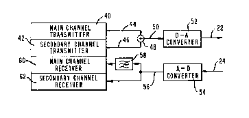
Referring now to Fig. 3, there is shown a
block diagram of the transmitters and receivers in the
control modem 12, with the corresponding configuration
for the tributary modems 14, 16, 18 being identical to
that shown in Fig. 3. Referring first to the
transmitter portion, the main channel transmitter 40
and the secondary channel transmitter 42 transmit
signals on respective output lines 44, 46, which
signals are added in an adder 48 whose output is
connected over a line 50 to the input of a digital-to-
analog converter 52 which has an output coupled to the
transmit line 22.
The receive line 24 is connected to an
analog-to-digital converter 54 whose output is
connected over a line 56 to a digital notch filter 58,
the output of which is coupled to the main channel
receiver 60. The notch filter 58 is a band-stop
digital filter which eliminates the secondary channel
signal (300-350 Hz band) and passes the main channel
signal (600-3000 Hz band) to the main channel receiver
60. Thus, the notch filter 58 acts as a high-pass
filter, but a notch filter is used since the
implementation is simpler than a high-pass filter.
The construction of such notch filters is well known
and will not be described herein.
The output line 56 of the analog-to-digital
converter 54 is also connected to the secondary
channel receiver 62 wherein filtering is effected to
achieve a high suppression of the main channel signal,
in a manner which will be described in detail
hereinafter.
~2~?7599
6 --
Referring now to Fig. 4, there is shown a
block diagram of the secondary channel transmitter 42
(Fig. 3). A signal representing a mark or space
symbol (e.g. high or low level signal3 is applied on
an input line 70 to a complex signal generator 72.
The complex signal generator 72 is a binary continuous
phase FSK modulator, that is, frequency shift keying
with phase turns corresponding to two frequencies and
with continuous phase changes between successive
symbol intervals. The use of continuous phase FSK
modulation results in less bandwidth being used,
whereby the influence of noise and distortion is
restricted. The complex signal generator 72 produces
complex-valued samples at 9600 Hz on an output line
74. It should be understood that throughout the
drawings, a double line interconnection is used for
complex-valued quantities and a single line
interconnection for real-valued quantities. Each
complex-valued signal sample has, with regard to the
previous sample, a phase turn of -2 ~ 20/9600 or +2 ~
30/9600 radians, corresponding to a negative Erequency
of -20 Hz and a positive frequency o~ +30 Hz,
respectively, according to whether the signal on the
input line 70 represents a mark symbol or a space
symbol. A mark symbol corresponds to 128 phase turns
of -2 ~ 20/9600 during the symbol int.erval and a space
symbol corresponding to 128 phase turns of +2 ~
30/9600 during the symbol interval. After each symbol
interval (1/75 sec, 128 samples), the same symbol and
corresponding phase turns can occur or the other
symbol and corresponding phase turns can occur.
The complex output of the complex signal
generator is applied over line 74 to an IIR (Infinite
Impulse Response) digital low~pass filter 76, which
removes signal components from the spectral side
lobes, which could disturb the main channel signal.
Referring briefly to Fig. 5, the IIR filter 76
~?7~S99
includes adders 90, 92, multipliers 94, 96, 98 and a
delay unit 100, connected in the manner shown in Fig.
5 by complex-valued signal lines. In a preferred
embodiment, the coefficients have the values:
Cll = 0.02395
C12 = 0.95209
C13 = 0.5
These coefficients are determined by selecting
initially an analog low-pass filter with minimal
effect on the secondary channel in-band components
(-37.5 Hz to +37.5 Hz) and high suppression of out-
band components above 150 Hz. Then, in a well-known
manner, the analog low-pass filter is converted to a
digital low-pass filter.
Returning to the description of Fig. 4, the
complex-va]ued output of the IIR filter 76 is applied
over line 78 to a frequency converter ~0 having the
form of a co~plex multiplier, which receives over a
line 82 a signal exp(+j2 ~ (320n/9600)) which
represents a complex-valued carrier signal of 320 Hz
for successive samples at a 9600 Hz sample rate. The
fre~uency converter multiplier 80 produces real-valued
signal samples on an output line 84. It will be
appreciated that the frequency converter 80 acts to
effect a spectral shift of 320 Hz in the signal
spectrum. Referring briefly to Fi~. 6A, there is
shown the signal spectrum of the signal at the input
of the IIR filter 76. This signal spectrum is
centered around 0 Hz. Fig. 6B shows the signal
spectrum on the output line 84 of the frequency
converter 80, after spectral shift and removal of the
side lobes, and is a more precise representation of
the dashed line 32 in Fig. 2 in showing the general
shape of the secondary channel signal spectrum. The
output line 84 is coupled to the line 46 (Fig. 3)
whereby the real-valued signal samples of the
secondary channel are added by the adder 48 to real-
~ 2~7~99
valued samples on the output line 44 of the mainchannel transmitter 40, Eor application to the
digital-to-analog converter 52. It should be
understood that the main channel transmitter 40 also
operates at a 9600 Hz sample rate.
The filtering operation in the secondary
channel receiver 62 (Fig. 3) will now be described
with particular reference to Figs. 7 and 9. Fig. 7
illustrates the theoretical basis of the fi~tering
operation, whereas Fig. 9 shows the practical
implementation for such filtering operation.
Referring first to Fig. 7, the signal on the line 56,
from the analog-to-digital converter 54 (Fig. 3), is
applied to a low-pass IIR digital filter llOA, wherein
the signal is processed at the 9600 Hz sample rate,
while frequencies above 800 Hz are eliminated. At the
output of the filter llOA every fourth sample is
selected to provide a real-valued signal having a
sample rate of 2400 Hz which appears on an output line
112 of the filter llOA. This reduced sample rate
signal on line 112~ is applied to a frequency converter
114 appearing in the form of a multiplier, to which an
input signal exp(-j.2 ~ (320.n.4./9600)~ is applied on
a line 116. The resulting complex-valued output
signal is applied over a line 118 to a low-pass IIR
digital filter llOB, which is identical to the filter
llOA, but is processed at a 2400 Hz rate. The filter
llOB eliminates frequencies above 200 Hz,
corresponding to main channel components above 520 Hz
before the frequency conversion occurs in the
frequency converter 114.
At the output of the filter llOB, every
alternate (even) sample is selected to provide a
sample rate of 1200 Hz on a line 120. The signal on
the line 120 is applied to a low-pass IIR digital
filter llOC, which is iden~ical to the filters llOA
and llOB, but is processed at a 1200 Hz rate. The
~ 7S~9
g
filter llOC eliminates frequencies above 100 Hz,
corresponding to main channel components above 420 Hz
before the frequency conversion occurs in the
frequency converter 114. At the output of the filter
llOC, every alternate (even) sample is selected to
provide a 600 Hz sample rate signal which is applied
on a line 122 to a detector 124, which will be
described in more detail hereinafter, and which
provides an output signal representing the detected
data bit on an output line 126. In connection with
the foregoing description of the filters llOA, llOB,
llOC, it will be appreciated that each of the filters
eliminates frequencies greater than 0.08 times the
sample rate at which the filter is processed. Thus,
all frequency components above half of the new sample
rate are eliminated, whereby degradation by aliasing
(frequency fold over) is avoided. Furthermore, since
the filters llOA, llOB, llOC are processed at sample
rates of 9600 Hz, 2400 Hz and 1200 Hz respectively,
the low-pass behavior of the filters has transition
bands at 500-800 Hz, 125-200 Hz and 62-100 Hz
respectively. For such filters, the behavior relative
to the sample rate is the same. Thus, such filtering
makes it possible to use a relatively simple filter
with a low cut-of frequency and a small transition
band.
An understanding of the secondary channel
receiver filtering operation described above is
assisted by reference to Figs. 8A, 8B and 8C. Fig. 8A
is a plot showing signal spectrum level against
frequency at the input to the filter llOA. The solid
line segments 130, 132 represent the main channel
signal spectrum. The dashed line segments 134, 136
represent the secondary channel signal spectrum, and
the dotted line segment 138 represents the filter
characteristic.
~ ~75~9
-- 10 --
E'ig. 8B is a plot showing signal spectrum
level against frequency at the input to the filter
llOB. The solid line segments 140, 142 represent the
main channel signal spectrum, the dashed line segments
144, 146 represent the secondary channel signal
spectrum and the dotted line 148 represents the filter
characteristic.
Fig. 8C is a plot showing signal spectrum
level against frequency at the input to the filter
llOC. The dashed line 150 represents the secondary
channel signal spectrum and the dotted line 152
represents the filter characteristic.
The processing effected in the filters llOA,
llOB and llOC during one symbol interval of 1/75 sec.
is illustrated in the following Table A:
Table A
FilterProcessing EffectedOutput Samples Used
llOA128 times at 9600 Hz 32
llOB32 times at 2400 Hz 16
llOC16 times at 1200 Hz 8
The filters llOA, llOB and llOC have the same
structure and the same coefficients. This enables a
single filter to be utilized in the implementation of
the filtering operation described with reference to
Fig. 7. Such an implementation is shown in Fig. 9,
which illustrates the manner in which a slngle IIR
digital filter 110 is employed in the preferred
embodiment of the invention to effect the processing
described theoretically with reference to Fig. 7.
Referring now to Fig. 9, the IIR filter 110
which performs the functions of the filters llOA, llOB
and llOC (Fig. 7), is shown connected between an input
line 160 coupled to a three-position input switch 162
and an output line 164 coupled to a three-position
output switch 166. Also provided is a third three-
position switch 168 whose three terminals are
5~
connected to respective storage devices 170, 172 and
174. The storage devices 170, 172 and 174 are
utilized to store internal samples from delay elements
in the filter 110 corresponding to the time intervals
during which the filter 110 is utilized for processing
at the different processing rates, as described
hereinafter. It should be understood that the
switches 162, 166 and 168 are operated synchronously
such that the corresponding terminals having positions
labelled 1, 2 and 3 thereof are effective
simultaneously.
It should be understood that the filters
llOA, llOB and llOC shown in Fig. 7 correspond to the
filter 110 (Fig. 9) with the switches 162, 166 and 168
in positions 1, 2 and 3 respectively. For a sample
interval of 1/9600 second with the switches 1~2, 166
and 168 in position 1, the stored values of the delay
elements are read out from the storage device 170 and
supplied to the delay elements in the filter 110. The
filter is then processed and the new contents of the
delay elements are stored in the storage device 170.
For each fourth sample interval with switch 166 in
position one, the output of the filter 110 is used as
the input to the frequency converter 114. With the
switches in position 2, the input to the filter 110 is
derived from position 2 of the input switch 162 and
the contents of the storage device 172 are read into
the delay elements in the filter 110. The filter is
then processed and the contents of the delay elements
are read out and stored in the storage device 172.
For the odd output samples of the filter 110
with the switches in position 2, there is a return to
processing in switch position 1, but for each even
output sample of the filter 110 the output sample of
the filter with the switches in position 2 is used
(once per 8 intervals of 1/9600 second) as the input
of the filter 110 with the switches in position 3.
12~75~9
- 12 -
Thus, with the switches in position 3 the contents of
the storage device 174 are read into the delay
elements in the filter 110, the filter is processed
and the contents of the delay elements are stored in
the storage device 174.
For the odd output samples of the filter 110
with the switches in position 3, there is a return to
processing of the filter 110 with the switches in
position 1, but for each even output sample of the
filter in position 3 the output sample of the filter
is used (once per 16 intervals of 1/9~00 second) as
the input to the detector 124.
Fig. 10 shows an implementation for the IIR
low-pass filter 110 shown in Fig. 9. The filter 110
is connected between the input line 160 and the output
line 16~ and includes adders 180-210 inclusive,
multipliers 212, 214, 216, 218 and 220 utilizing
coefficients C21, C22, C23, C24 and C25 respectively,
and delay elements 222-230 inclusive. The various
components of the filter 110 are interconnected in the
manner shown in Fig. 10. The IIR low-pass filter 110
is an elliptic type filter and the design of the
filter 110 is preferably in accordance with the
principles and filter structures discussed in an
article by R. Ansari and B. Liu "A Class of Low Noise
Computationally Efficient Recursive Digital Filters",
Proceedings of the IEEE International Symposium on
Circuits and Systems, April 1981, pages 550-553. The
values of the coefficients utilized in the preferred
embodiment of the invention are as follows:
C21 = -0.79235
C22 = 0.91922
C23 = -0.94024
C24 = 0.74005
C2s = -0.95751
These coefficients are derived by elliptic filter
design techniques with the desired requirements for
~ ~?7599
- 13 -
pass- and stop- band behavior, as discussed in the
aforementioned article by Ansari and Liu, and in
another article by the same authors, entitled "A Class
of Low-Noise Computationally Efficient Recursive
Digital Filters with Applications to Sampling Rate
Alterations", IEEE Transactions on Acoustics, Speech
and Signal Processing, vol ASSP-33, No. 1, February
1985, pages 90-97.
Referring now to Figs. llA and llB there are
shown plots which illustrate the transfer function
(amplitude distortion in Fig. llA and delay distortion
in Fig. llB) of the total secondary channel
transmission path, including telephone line
distortion. In Fig. llA, (amplitude distortion), the
solid line 240 represents no distortion and the dashed
line 242 represents worst case distortion. In Fig.
llB, (delay distortion), the solid line 250 represents
no distortion and the dashed line 252 represents worst
case distortion. For different telephone lines,
amplitude and delay distortion at 300 Hz relative to
such distortion at 350 Hz will vary as follows:
amplitude distortion: 0 to 1.5 dB
delay distortion: 0 to 1.3 msec.
The total amplitude and delay characteristic of the
filtering in the secondary channel transmitter and
receiver is centered around 320 Hz. This gives
differences in amplitude and delay characteristic at
300 Hz relative to those at 350 Hz as follows:
amplitude characteristic: -0.5 dB
delay characteristic: -0.3 msec.
Hence, the total, composed of contributions from
transmitter filtering, telephone line distortion and
receiver filtering for different telephone lines at
300 Hz relative to 350 Hz, will vary as follows:
amplitude distortion: -0.5 to 1.0 dB
delay distortion: -0.3 to 1.0 msec.
~ 2~
- 14 -
Thus, it will be appreciated that the filtering
provided in the preferred embodiment achieves
precompensation for differences in distortion between
300 Hz and 350 Hz and hence enables a more reliable
detection for telephone lines where a high level of
distortion is introduced.
Referring now to Fig. 12, there is shown a
block diagram of the detector 124 shown in Figs. 7 and
9. The detector 124 has an input line 122 which is
coupled to a -20 Hz correlator 260 and a +30 Hz
correlator 262. The -20 Hz correlator 260 includes a
multiplier 264 which receives the input signal from
the line 122, at a 600 Hz sample rate, and, over a
line 266, the following multiplication factor:
exp(-j.2 ~ (-20.1.16)/9600),
where 1 = 0, 1,....7.
The output of the multiplier 264 is connected to an
adder 268 which effects successive additions for 8
successive samples, according to the formula:
~ sK+l exp(-j2 ~ (-20/600)1
Q=0
once per 1/75 second, with 8 input samples
Sn = Sk, Sk+l ~----Sk+7-
The +30 Hz correlator 262 includes a
multiplier 270 which receives the input signal from
the lines 122, at 600 Hz, and, over a line 272, the
multiplication factor:
exp(-j.2 ~ (30.1.16)/9600),
where 1 = 0, 1,....7.
The output of the multiplier 270 is connected to an
adder 274 which effects successive additions for 8
successive samples according to the formula:
~ sK+l exp(-j2 ~ (~30/600)1
1=0
once per 1/75 second, with 8 input samples
Sn = Sk, Sk+l ~ Sk+7-
~75~9
- 15 -
The complex-valued outputs 276 and 278 of the
respective adders 268, 274 carry signals at a 75 Hz
rate and are connected to a norm comparator 280. In
the norm comparator 280 the squared vector lengths of
the correlator outputs are calculated and compared.
The norm comparator 280 then decides if during the
last 1/75 second, a -20 Hz signal was more likely to
occur than a +30 Hz signal as the input to the
detector 124. Thus, with:
correlator 260 output = xl + j Yl
correlator 262 output = X2 + i Y2
the squared vector lengths:
vl2 = xl + Yl
V22 = X2 + Y2
are calculated. If vl2 > v22 then a -20 Hz signal
corresponding to a mark symbol is detected. If vl2 <
V22 then a +30 Hz signal corresponding to a space
symbol is detected.
The above description refers to the normal
operation of the detector 124 during signal
transmission. However, in order to provide an
efficient initial detection when an initial pattern
consisting of 14 mark symbol followed by 2 space
symbols is transmitted, both correlators are initially
tuned to -20 Hz, but with a half-symbol shift (1/150
sec) timing difference. Thus, in the correlator 260
the adder 268 effects the addition:
~ sK+l exp(-j2 ~ (-20/600)1)
1=0
and in the correlator 262, the adder 274 effects the
addition:
~ SK+4+1- exp(-j2 ~ (-2o/6oo)l)
Q=0
When correlation to -20 Hz falls down, corresponding
to a space symbol being present, the correlator 262 is
changed to correlate at +30 Hz by changing the input
signal on the line 272. Thus, an optimal first sample
~ ~75~3
- 16 -
to start the normal operation of the detector 124 is
derived, based on the aforementioned fall down of the
correlation to -20 Hz. Hence, the two correlation
measurements during subsequent normal operation of the
detector 124 are made with appropriate timing.
Summarizing, it will be seen that the
preferred embodiment of the invention includes a
secondary channel receiver which is implemented by
digital complex-valued signal processing and has the
advantage of using a minimum amount of circuitry while
achieving a high performance. Thus, only a single
analog-to-digital converter is needed at the receiving
modem, since the same signal samples are used for the
secondary channel receiver as for the main channel
receiver. Furthermore, accurate filtering and high
suppresslon of main channel signal frequencies is
achieved without aliasing (frequency fold over) by
using a single filter which is processed a number oE
times at different sample rates. Moreover, the
signalling and timing in the secondary channel are
independent of the main channel and the secondary
channel operates without interference from the channel
and without causing degradation in the main channel
during secondary channel transmission.
While the salient features of the invention
have been illustrated and described, it should be
readily apparent to those skilled in the art that many
changes and modifications can be made in the invention
presented without departing from the spirit and true
scope of the invention. Accordingly, the present
invention should be considered as encompassing all
such changes and modifications of the invention that
fall within the broad scope of the invention as
defined by the claims.