Note: Descriptions are shown in the official language in which they were submitted.
~2~794~3
OZONE GAS SENSOR AND OZONE GAS ~ETECTING DEVICE IIAVING
OZONE GAS SENSOR
BACKGRO~ND OF THE INVENTION
(1) Field of the Invention
The present invention rela-tes to an ozone gas
sensor and an ozone gas detecting device having the
ozone gas sensor.
(2) Description of the Prior Art
A conventional ozone gas sensor comprises a film
type semiconductor element including an insulating
substrate such as of alumina and a semiconductor film
consisting of a metallic oxide formed on the
substrate, and a layer of silica formed on a surface
of the film type semiconductor element. The
semiconductor film of a metallic oxide allows ozone
gas having high reactivity to reach a sensing section
of the sensor without decomposing on the surface of
the semiconductor film. The layer of silica formed on
the semiconductor element promotes sensitivity to
ozone gas.
Such an ozone gas sensor has the followin8
problem when used in the presence of both ozone gas
and a reducing gas:
Where the f ilm type semiconductor element
comprises an n-type semiconductor, the resistance of
-1-
~L~9~8
-the semiconductor increases through contact w;th ozone
~as and decreases through contact with -the reducing
gas, thereby rendering measurement results inaccurate.
Conversely, where the film type se~iconductor eleMent
comprises a p-type semiconductor3 the resis-tance of
the semiconductor decreases through contac-t with ozone
gas and increases through contac-t with the reducing
gas. In either case, measurement results are
inaccurate, being lower than actual levels or
dispersed.
Consequently, an ozone gas detecting device
incorporating such an ozone gas sensor has low
sensitivity and precision in the presence of a
reduc-tion gas.
SUMMARY OF THE INVENTION
Having regard to the state of the art noted
above, an object of the present invention is to
provide an ozone gas sensor which is easy to handle,
inexpensive, and capable of measuring ozone gas with
high sensitivity even where ozone~ gas and a reducing
gas coexist.
In order to achleve the above object, an ozone
gas sensor according to the present invention
comprises a filM type seMiconductor eLement including
a substrate and a semiconductor film consisting of a
. --2-- -
~2~
metallic oxide formed on the substrate, and a layer of
silica formed on a surface of the film type
semiconductor element, wherein at least one thin film
layer of one or a plurality of types selected from
metals and metal oxides is interposed between the
semiconductor film and the layer of silica.
At least one thin film layer of one or a
plurality of types selected from metals and metal
oxides interposed between the semiconductor film and
the layer of silica is effec-tive to prevent a
substantial reduction in the sensor output responsive
to ozone gas in the presence also of a reducing gas.
The thin film layer or layers may be formed
between the semiconductor film and the layer of silica
by an ordinary film forming technique without
requiring a special technique or an expensive
apparatus.
l'he present ;nvention -thus provides an ozone gas
sensor easy to handle, inexpensive and capable of
high-sensitivity and high-precision measurement.
An ozone gas detecting apparatus incorporating
this ozone gas sensor is also easy -to handle,
inexpensive and highly sensitive.
Other advantages of the present invention will be
apparent from the detailed description of the
preferred embodiments to follow.
.
--3--
12g7~48
BRIEF DESCRIPI`ION OF TIIE DRAWINGS
The drawings illustrate ozone gas sensors and
ozone gas detecting devices having these ozone gas
sensors according to the present invention, in which:-
5Fig. 1 is a schematic sectional view showing the
principle of a semiconductor type ozone gas sensor,
Fig. 2(a) through 2(d) are graphs showing
response waveforms and output reductions of various
ozone 8as sensors in the presence of both ozone gas
10and ethyl alcoho] gas,
Fig. 3 is a sectional view of a semiconductor
type ozone gas sensor according to another embodiment
of the invention,
Fig. 4 is a sectional view of a semiconductor
15type ozone gas sensor according to a further
embodiment of khe invention,
Fig. 5 is a sectional view of a semiconductor
type ozone gas sensor according to a still further
embodiment of the invention,
20Fig. 6 is a front view of an entire ozone gas
detecting device,
Fig. 7 is a block diagram showing a
constructionaL outline of the ozone gas detecting
device shown in Fig. 6,
25Fig. 8 is a perspective view of a modified ozone
gas det~cting device,
--4--
~79~L~
Fi8. 9 is a block diagram showing a
constructional outline of the ozone gas detecting
device shown in Fi8- ,
Fig. 10 is a view showing the principle of an
ozone gas sensor of the potentiostatic electrolysis
type which is one example of ozone gas sensor
incorporated into the ozone gas detecting device shown
in Fig. 8, and
Fig. 11 is a graph showing output variations of
the potentiostatic electrolysis type ozone gas sensor
shown in Fig. 10.
DETAILED DESCRIPTION OF THE PREFERRED EMBODIMENTS
Ozone gas sensors and ozone gas detecting devices
having the ozone gas sensors according to the present
invention will be described in detail hereinafter with
reference to the drawin8s~
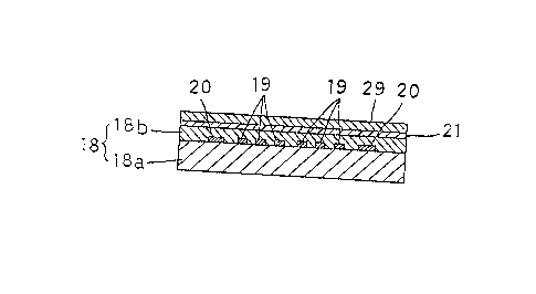
Fig. 1 is a schematic sectional view of a
seniiconductor film type ozone gas sensor. This sensor
comprises a film type semiconductor element 1~, a thin
film layer 21 formed on the semiconduc-tor element lo,
and a layer of silica (SiO ) 29 ~ormed on the thin
fillll Layer 21.
The semiconductor element 18 may comprise an
.insulating substrate l~a consisting of alumina or the
:Like, and a semiconductor film l~b formed on the
substrate lBa and including indium oxide (In O ), tin
2 3
oxide (SnO ), zinc oxide IZnO) or other metallic oxide
as a main component thereof. The thin film layer 21
comprises a single layer or a plurality of layers of
one or different -types selected from metals and
metallic oxides. The metals available for use include
palladium, platinum and the like, while the metallic
oxides include oxides of chromium, manganese, iron,
cobalt, palladium, platinum, copper and other
transition metals. The thin film layer 21 may have a
single layer or multilayer construction comprising a
combination of a metal and an oxide similar thereto, a
combination of a metal and an oxide dissimilar
thereto, or comprising a single metal or a plurality
o metals, or a single metallic oxide or a plurality
of metallic oxides. The thin film layer 21 may be
formed on the film type semiconductor element 18 by
the thermal decomposition, chemical deposition,
physical deposition or o-ther method used for forming a
metal compound or compounds into a film.
~ layer of silica 29 is formed on the thin film
layer 21 as noted above. This layer 29 is formed by
chemically depositing an organic silicon compound such
as hexamethyl disiloxane on the thin film layer 21.
Number l9 in Fig. 1 indicates a comb-shaped
electrode embedded between ~he insulating substrate
--6--
1~7~
18a and semiconductor film 18b, and number 20
indica-tes a hea-ter attached to a back surface of the
insulating substrate 18a.
Sensor output variations occurring in the
presence of both ozone gas and ethyl alcohol gas which
is a reducing gas will be described next. Fi~s. 2(a)
through 2(d) schematically show response waveforms and
reductions in the ozone gas sensitivity of various
ozone gas sensors described below, in the coexistence
of ozone gas and ethyl alcohol gas. The sections
marked by ~ in these drawings represent the
coexistence of ozone gas and ethyl alcohol gas.
Fi8. 2(a) shows the case of using an ordinary
ozone gas sensor having the metallic oxide
semiconductor film l~b formed on the insulating
substrate 18a. Fig. 2(b) shows the case of using a
sensor having the thin film layer 21 of a metallic
oxide formed on the film type semiconductor element
1a. Fig. 2(c) shows the case of using a sensor having
the layer of silica 29 formed on the film type
semiconductor elernent 1~. Fi8. 2(d) shows the case of
using the film type ozone gas sensor according to this
embodiment.
It will be seen that the sensor outpu-t
deteriorates in the coexistence of ozone gas and ethyl
alcohol gas where the thin film layer of a metallic
.
-7-
oxide is formed (Fig. 2(b)) on the ordinary film type
semiconductor element (~ig. 2(a)). ~here the layer of
silica is formed (Fig. 2(c)) on the ordinary film type
semiconductor element (Fig. 2(a)), the sensor output
increases in the absence of ethyl alcohol gas but no
significant improvement is seen as regards the output
in the coexistence of ozone gas and ethyl alcohol gas.
By contrast, the ozone gas sensor according to this
embodiment (Fig. 2(d)) shows a 8reat improvement with
respect to the output reduction in the coexistence of
ozone gas and ethyl alcohol gas. It has thus been
confirmed that, by interposing the thin film layer of
a metallic oxide between the film type semiconductor
element and the layer of silica, the output reduction
is effectively chec~ed in the coexistence of the two
gases while substantially sustaining the sensor output
responsive to ozone gas in the absence of ethyl
alcohol gas.
The present invention will particularly be
described next with reference to experiments
conducted.
[Experiment ~]
Film type ozone gas sensors were manufactured,
each of which comprised a film type semiconduc-tor
element havin8 indium oxide as the main component
thereof and prepared by the vacuum deposition method,
--8-- .
and a thin film layer or layers of a me-tallic oxide,
different metallic oxides or a metal and metallic
oxide combination formed on the semiconductor element.
The thin film layer was formed by applying to the
semiconductor element a metallic salt solution of one
of the metals listed in Table 1 below) and drying and
baking the product. Each sensor further comprised a
layer of silica formed by chemically depositing
hexamethyl disiloxane on the thin film layer.
Each ozone gas sensor thus manufactured was
exposed to a mixture of ozone gas and ethyl alcohol
gas to measure the sensor outpu-t responsive to
standardized ozone gas. Results of the measurement
are shown in the righthand column of Table 1. The
results confirm that the sensors according to this
invention employing any one or more of the listed
~etals and their oxides are effective for checking the
output reduction in the presence of a reducing gas.
~9~79~
Table 1
_ Sensor Output in O and
C H OH
Metallic Oxide Layers
Sensor Output in O
Cr Oxide 0.23
_
Mn Oxide 0.72
Fe Oxide 0.68
Co Oxide 0.90
Pd and/or Pd Oxide 0.30
Pt and/or Pd Oxide 0.4
Cu Oxide 0.91
.... ..... ~.
Ce Oxide 0.49
. .. _ . ___
~Co+Cu) Oxide 0.95
_
Ce Oxide Layer
+ Fe Oxide Layer 0.70
_ _ _ I
None 0.13
.. _ _. ._
[Experiment 2]
Film type ozone gas sensors were manufactured,
each of which comprised a film type semiconductor
element having tin oxide as the main component thereof
and prepared by the vacuuln deposition method, and
thin film layer or layers oE a metallic oxide,
; different metallic oxides or a metal and metallic
. , --10--
12~
o~ide combination formed on the semiconductor element.
The thin film layer was formed by applying to the
semiconductor element a metallic salt solution of one
of the metals listed in Table 2 below, and drying and
baking the product. Each sensor further comprised a
layer of silica formed by chemically depositin~
hexamethyl disiloxane on the thin film layer.
Each ozone gas sensor thus manufactured was
exposed to a mixture of ozone gas and ethyl alcohol
gas to measure the sensor output responsive tb
standardized ozone gas. Results of the measurement
are shown in the righthand column of Table 2. The
results confirm that these sensors are also effective,
by virtue of the thin film layer, for checking the
output reduction in the presence of a reducing gas
although slightly less effective than in Experiment l.
. .
129~9~3
_ Table 2 _ _
Sensor Output in O and
C H OH
Me-tallic Oxide Layers
Sensor Output in O
Cr Oxide 0.17
Mn Oxide 0.6B
.
Fe Oxide 0.65
.Co Oxide 0 87
Pd and/or Pd Oxide 0.35
Pt and/or Pd Oxide 0.54
Cu Oxide 0.8~ .
Ce Oxide 0.44
_
(Co~Cu) Oxide 0.93
Ce Oxide Layer
Fe Oxide l.ayer 0.65
._ _ - -- ''I
None 0.11
. . _- ,
[EXperiment 3]
Filrn type ozone gas sensors were manufactured,
each of which comprised a film type semiconductor
element having zinc oxide as the main component
thereof and prepared by the vacuum deposition method,
and a thin filrn layer or layers of a metallic oxide,
different metallic oxides or a metal and metallic
-12-
' ' '
~ . ,
~2~
oxide combination formed on the semiconductor element.
The thin film layer was formed by applying to the
semiconductor element a metallic salt solution of one
of the metals listed in Table 3 below, and drying and
baking the product. Each sensor further comprised a
layer of silica formed by chemically depositing
hexamethyl disiloxane on the thin film layer.
Each ozone gas sensor thus manufactured was
exposed to a mixture of ozone gas and ethyl alcohol
gas to measure the sensor output responsive to
standardized ozone gas. Results of the measurement
are shown in the righthand column of Table 3. The
results confirm that these sensors are also effective,
by virtue of the thin film layer, for checking the
output reduction in the presence of a reducing gas
although slightly less effective than in Experiment 1.
-13-
.. , .. ~
Table 3
_ ~ Sensor Output in O and
C2H50H
Metallic Oxide Layers
~ensor Outpu-t in O
Cr Oxide 0.20
Mn Oxide 0.75
Fe Oxide 0.65
Co Oxide 0.85
Pd and/or Pd Oxide 0.34
Pt and/or Pd Oxide 0.50
_ _ _
Cu Oxide 0.90
Ce Oxide 0.51
~Co+Cu) Oxide 0.91
_ .... _ . _ ...
Ce Oxide I.ayer
+ Fe Oxide Layer 0.71
. .
None 0.12
. . ~
Ozone gas sensors according to other embodiments
of the invention will be described next.
As shown in Fig. 3, the comb-shaped electrode 19
and the heater 20 may be formed on the same surface of
the insulatin~ substrate lBa, the electrode 19 bein~
covered by the semiconductor film lBb formed on the
substrate 1Ba. The heater 20 may be embedded in the
-14-
: ' . . .. . ..
. .
lZ~79~
substrate l~a.
As shown in Fig. 4, an electrode 19 acting also
as a heater 20 may be formed on the insulating
substrate 1~a, with the semiconductor film 18b formed
on the substrate 18a to cover the electrode 19.
As shown in Fig. 5, an additional layer of silica
29 may be formed on the bac~ surface of the insulating
substrate 18a so as to cover the heater 20. This
construction, in addition to the foregoing advantages,
is effective, by means of the additional layer of
silica 29, to enclose surfaces of the heater 20 ou-t of
contact with air and thus providing a protection for
the heater 20. This heater 20 will retain stable
heating characteristics over a long period of ~lse, and
promote long-term reliability of the thin film type
ozone gas sensor.
In the above embodiments, the thin film layer is
interposed as a uniform layer between the film type
semiconductor element and the layer of silica. This
thin film layer, however, may cornprise a non-uniform
layer with a metal or metallic oxide dispersed in high
concentration, for example. ~urther, while the
fore~oing embocliments have been described in relation
to ethyl alcohol gas as an example of reducing gas
which affects the sensor output responsive to ozone
gas to the greatest extent, the ozone gas sensors
-15-
..
~2~7~
according to the present invention will produce the
same effects in the presence of other reducing gases
such as hydrogen, ammonia and methane gases.
The semiconductvr film formed on the substrate in
the described semiconductor type gas sensors may
comprise a metallic oxide having tin oxide (SnO ),
zinc oxide (ZnO) or ferric oxide (Fe O ) as a main
component. Further, the semiconductor film may
comprise indium oxide (In O ) included in at least one
of the above metallic oxides, or have indium oxide as
the main component. The semiconductor film having
indium oxide as the main component in particular has
high selecti~ity with respect to ozone gas (O ).
Figs. 6 and 7 illustra-te an ozone gas de-tecting
device having one of the described ozone gas sensors
according to the present invention.
This detecting device comprises a detector unit
containing an ozone gas sensor 7, and a casing 22
including an indicator 23 for providing a visual
display of measurement results, a zero adjuster ~nob
31 and a mode changec)ver switch 32 for varying
measurin~ ma8nification. The casing 22 houses a power
source 33 for electrifying the heater of the ozone gas
sensor 7 in the detector unit 30, a signal amplifier
34 for amplifying a signal received from the detector
unit 30, an amplifyine circuit power source 35 for
. . .
-16-
,
~12~
driving the signal amplifier 34, an internal power
source 36 and an AC adapter 37 for supplying power to
the amplifying circuît power s~urce 35 and the heater
power source 33, and an output unit 38 for outputting
data to be displayed by the indicator 23 and to be
recorded by a recorder and for giving an alarm. The
alarm may be given by a buzzer or a flashing color
lamp when ozone gas concentration exceeds a
predetermined level or falls below a predetermined
level or to zero. The indicator 23 includes a control
signal output circuit. The internal power source 36
normally comprises a battery. Either one or both of
the internal power source 36 and AC adapter 37 may be
provided. Although not shown, a source switch for
operating the detecting device is provided on an outer
wall of the casing 22, and a battery lamp for
indicating a battery operation and an output terminal
may also be provided as appropria-te.
Another example of ozone gas detectin~ device
will be described next with reference to Figs.
throllgh 1l.
This detecting device is a suction type device
and comprises a casing 22' includ;ng, as shown in Fig.
~, a first indicator 44 associated with an ozone gas
2S measuring sensor 5, a second indictor 24 associated
with an ozone gas removal. Fonfirming sensor 7', an
-17~
~z~
alarm buzzer 25 and an alarm lamp 26 operable through
an automatic control unit 9, a recovery section 27 of
a catalyzer 6, and a source switch 28. A gas intake
tube 1 extends from the casing 22, which intake tube 1
<~ f~~aS~ ~r7ar,~ 5 includes a flexible Teflon~tube lA and a stainless
steel tube 1~ connected to a distal end of the Teflon
tube lA. The ozone gas measuring sensor 5 is mounted
on a gas intake passage R for detecting ozone gas
concentration in the gas drawn through the gas intake
tube 1. The gas intake passage R communicates with an
intake port 4 of an electric suction pump 3 having a
gas exhaust port 2 opening to the ambient. The
stainless steel tube 1~ may be replaced with a Teflon
tube.
As shown in outline in Fig. 9, the gas intake
passage R includes the catalyzer 6 disposed between
the ozone gas measuring sensor 5 and the suction pump
3 for reducing ozone gas to oxygen gas, and -the ozone
gas removal confirming sensor 7' disposed between the
catalyzer 6 and the suction pump 3. The automatic
control unit 9 is operable to automatically turn off a
source c;rcuit B connected to the suction pump 3 only
when the ozone gas removal con~irmirlg sensor 7' gives
a detection result that the ozone gas concentration in
the gas having passed through the catalyzer 6 exceeds
a predetermined level. Instead of the construction
-lB-
, .
~2~
for causing the automatic control unit 9 to
au-tomatically turn off the source circuit 8 connec-ted
to the suction pump 3, a valve may be provided on the
intake passage R ups-tream of the suction pump 3 for
S stoppin~ the gas flow to the suction pump 3, the valve
being automatically closed when the ozone gas
concentration in the gas havin~ passed through -the
catalyzer 6 exceeds the predetermined level.
The gas intake tube 1 may include a filter formed
of alumina silicate at an inlet thereof for removing
gases and other matters obstructive to the
measurement.
The ozone gas measuring sensor 5 may be the
potentiostatic electrolysis type, or may be the
semiconductor type as illustrated in Figs. 1 and 3-5.
The gas sensor of the potentiostatic electrolysis
type, as shown in Fi8. 1l, is capable of detecting
o~one gas over a wide concentration range and is
particularly effective for detec-ting high
concentration ozone gas. On the other hand, the
semiconductor type g~s sensor is capable of detecting
low concentration oxone gas with hi8h sensitivity.
The potentiostatic electrolysis type gas sensor
5, as its principle is shown in Fig. 10, comprises a
working electrode 10, a reference electrode 11, a
co~lnter electrode 12, an electrolytic cell 14 filled
,
--19--
~7~L8
with an electrolyte 13, and a potentios-tat circuit 15.
Each of the electrodes 10, 11 and 12 comprises a gas-
permeable lnembrane 16 such as Teflon (PTFE) coated
with a noble metal catalyst. The electrolyte 13
comprises an acid solut.ion. The electroly-~ic cell 14
is formed of a plastic having high chemical
resistance, such as vinyl chloride.
Ozone gas having penetrated the gas-permeable
membrane 16 is reduced on a catalyst layer 17 of the
working electrode 10 through the following reaction:
O + 2H + 2e ~ O + H 0.
3 2 2
The water content (H O) is oxidized on the counter
electrode 12 through the following reaction:
i,/ H O ~ 1/2 0 + 2H + 2e .
2 2
Thus the following reaction takes place as a whole:
t 3/2 0~.
Ozone gas concentration is deterMined at this time by
measuring electrolytic current flowing in proportion
to the ozone gas concentration.
The catalyzer 6 should preferably comprise
manganese dioxicle (MnO ), cupric oxide (CuO) or the
li~e.
It is necessary for the ozone gas removal
confirming gas sensor 7' to reliably detect low
concentration ozone gas in particular. It is
therefore preferable to use the semiconductor type gas
-20-
sensor therefor
~ ith the suction ~ype ozone gas detecting device
having the foregoing construction, ozone gas in the
gas being detected is reduced to oxygen gas having a
low oxidiz;ng ability during passage through the
catalyzer after the ozone gas measuring sensor. Ozone
gas is thus prevented from being drawn into the
suction pump.
Where the suction pump is disposed immediately
downstream of the catalyzer, there is a danger of
ozone gas bein8 drawn into the suction pump when the
reducing capacity of the catalyzer diminishes or when
ozone gas passes through the catalyzer in an amount
exceeding the reducing capacity thereof. According
to the present invention, however, the automatic
control unit is operable to automatically stop the gas
drawing operation of the suction pump when the ozone
gas removal confirming sensor gives a de-tection result
that ozone gas remains in the gas having passed
through the catalyzer in an amoun-t exceeding a
predetermined level. ConsequentLy, the gas is neither
drawn into the suction pump nor released to ambient
air on such an occasion.
It is conceivabLe to use an oxidation resistant
material for a conventional suction pump. Such a
measure, however, would be more costly than providing
-21-
~L2~
the catalyzer, ozone gas removal confirming gas
sensor, and autoMatic control unit as in the present
invention. Moreover, such a measure would result in
the disadvantage of endangering people through
exposure to the gas released from the suction pump to
the ambient. By contrast, the present invention
allows the suction pump to be used reliably over a
long period, thereby providing ozone gas detecting
devices having excellent utility and economy.
- -22-