Note: Descriptions are shown in the official language in which they were submitted.
~2~ 8 83-~-137
CIRCUIT CONNECTOR FOR USE ~ITH PRINTED WIRING BOARD
BACBGROUND OF_TUE_INVENTION
l. FIELD OF_THE INVENTION
Thi~ invention relatea to mounting arrangementa for
printed circuit card~ or boards in electrical systems and
more particularly to a connector which is arranged to
~upport and retain in electrical connection a printed wiring
board.
2. DESCRIP'rION QF THE_RELATED_ART
Printed circuit cards or board~ have been u~ed for many
year~ in electronic equipment. The~e boards allow the many
electrical devices and components to be readily connected by
metallic circuits formed on one or more aurfaces of the
board. Today, much electronic equipment include~ plug-in
modu:le boards representing entire ~ub-sy~tem~ of electronic
apparatu~. The use of such an arrangement is of great
as~iatance in facilitat-ing as~embly and diagnostic
evaluation of circuit problems. Such circuit board~ are
usually provided with a plurality of electrical contact pad~
or connection~ along one edge of the card. The entire board
i~ then pre~-fitted into a ~pecinlly de~lgned edge
connector, having a plurality of mating contact~.
Electrical connection beteen the card ed~e connector and
o-ther device~ in the electrical apparatus i~ generally made
through means of ~eparate wiring.
~297~ 83-4-137
Although printed wiring card~ are pres~-fitted into
card edge connectors generally, these cOnDeCtiOns do not
grip the edge of the in~erted board wi-th any appreciable
strength. Since the printed circuit card may need to be
mounted horizontally, vertically or in some other
configuration, it i~ naturally ~ubject to ~ibration in many
environments. Thu~, it has generally been determined that
some form o-f support reten-tion mean~ must be provided in
order to securably hold the printed circuit board in
po~ition in its associated card edge connector.
Prior art apparatus generally have associated with each
card edge connector for ~upporting such printed wiring cards
one or more u-~haped channel~ for guiding and supporting the
printed circuit card. In this arrangement, the cards are
placed into the~e channel members which act to maintain the
printed circuit boards in a spaced apart, parallel or
similar relationship. It has also been determined that it
is not nece~sary to mercly guide the support for the circuit
cards but that each card must be securely Eastened or held
within thi~ channel in order to ensure that a proper
electrical connection i8 made and maintained between the
printed circuit boar-d card connector pads and the associated
card ed~e connector.
The usual solution to this problem i~ to include some
sort oE relea~able locking means a~sociated with the printed
circuit card ~o as to securely maintain the card within the
~7~5~ ~3-4-137
guide or support~ This arrangement then allows the mounted
card to be readily removed when de~ired. Such locking mean~
have taken many form~ ~uch a~ those di~clo~ed in U.S.
Patents 3,853,379, 3,767,974 and 3,764,8~7. These patents
all disclose a c~mming or lever locking mean~ provided in
the outward end of each channel guide which engages the
outer corners of the a~ociated printed circuit card. Other
technique~ were di3closed in such patents as U.S. 3,798,507,
3,784,954, 3,863,113, 3,741,513 and 3,715,630.
All of the above rely in some way to engage the support
and the card by means of a form of locking device or by a
similar technique. Most of the above techniques require a
special or modified type of printed circuit card to be u~ed
with the locking and guiding means or a speci~l latching
device or devices and associated u-~haped channel guides for
each printed circui-t card to be mounted.
SUMMARY_OF_THE_INVENTION
The above and other problems of prior art arrangement~
are overcome in the pre0ent invention by providing a
connector contact scheme, wherein indivi<lual prirrted circuit
card~ are in~erted into card connectors with the a3~istance
of card ¢uides which extend out from the face of the
connector. While these card guides help to support the line
cards after they are in~erted, they provide nothing to
overcome the effect of vibration or movement, wherein the
1~ 9~ 95 ~ 83-4-137
cards frequently would 7'walk" out of their plugged
connections.
In the pres~nt arrangemen-t, printed circuit card~ were
designed as line card~ for use in automated telephone
sy~tems. Since the total mass of each individual prin-ted
circuit card i~ relatively small~ a slight amount of card
retaining force could be incorporated into each individual
contact. Thus, the multiplicity of contact~ as~ociated with
each printed wiring card would be able to generate more than
an adequate amount of retention force required to maintain
the connection for each priDted circuit card.
In the perceived arrangement, the two-piece connector
system includes a movable contact located on the printed
circuit card and a fixed contact located in the printed
circuit card connector located on the -front edge of ths
motherboard or back plane of the electronic e~uipment.
While ~everal di-fferent contact arrangements are ~hown, they
all include the arrangement of a movable and a fixed
contact, wherein each of the contact~ have an embossed or
depressed area and the blade portion of each contact i~
~eparated by a particular di~tHnce. The embossed or ralsed
area on the movable contact has a leadinK anKle and a
trailing angle relative to the flat blade portion of the
contact. It i~ -thi~ leading angle which control~ in~ertion
force and the trailing angle controls extraction force in
; the contact ~ystem.
~ 7~ 3-4--137
During ~ating, the movable and ~ixed contacts are
caused to f:lex and separate due to the e~bossed or raised
portion on -the movable contact and when the contacts are
fully mated, -the embos~ed or raised portion of the movAhlc
contact nests in the embossed or opening of the fixed
coDtact and the blade portion o-~ both contacts are separated
by a particular distance.
In the case o-f a printed circuit card equipped with a
large number of movable contacts, vibration ~ay cau~e it to
"walk" out of its plugged position. However, its nested
embosses or raised portions would force the contact blade~
apart. Thus, the contact force would increase which in turn
; would then tend to maintain the two raised portions in the
nested or retained position. In e-f~ect, the electrical
contacts are also the mechanical means by which the printed
circuit boards are kept in their plugged positions. In
commercial application, the retention forces would be made
large enough to prevent the printed circuit boards -from
"walking" but low enough to keep card extraction forces
reasonable when a printed circuit board i~ purposely
withdrawn.
Several d:iff`erent blade contact confi~urations are
anticipated under the ternl~ of the present invention,
includlng the utilization of a stif.~ contract with leading
26 and trailing wedge-type edges and an associated ~lot in the
movable con-tact. Another approach would include contacts
129795B ~3-~-137
with convex and concave dimpled areas and conventional flat
~prings with curved sections included therein.
BRIEF DESCPIPTI0N OF THE_DRAWINGS
FIG. 1 i~ a partially cut out per~pective view of a
plurality of printed circuit boards and a~ociated
connector~ and supports including retention type contact~ in
accordance with the present invention.
FIG~. 2A, 2B and 2C show traditional -flat CODtaCt~ with
curved portion~ therein of each arranged prior to mating,
during mating and with the contact~ mated all in accordance
with the pre~ent invention.
FIG. 3 ~howA contactA in accordance with the preAent
invention employing convex and concave dimpled area~.
FIC. 4 Ahow~ cODtactA in accordance with the present
invention employing a ~tiff contact having a ramp-like
configuration and an as~ociated ~pring contact including a
Alot for receiving the joinder of the two ramp portion~ of
the 0tiff contact.
DEscRIp-T-IQN-QE-TNE~-pFlEFERRED-EMBoDIMENrr
The connector contact ~cheme of the pre~ent invention
wa~ designed t`or u~e in pac:}saging a Aolld-~tate line -frame
for u~e in the CTD-~ EAX Digital Telephone Sy~tem
manufactured by GTE Communlcation Sy~temA Incorporated. The
technique of packaging line circuit~ into a frame in a
Apace-~aVing and co~t- effectlve manner i~ of prime
importance ~ince the line frame~ make up typically 50-60% of
~z~
83-4-137
all the frames included in a modern telephone central
o~fice. Thu~, it will be apparent that the cost of the line
~rame may very well impact the sy~tem cost by more than any
other ~rame required throughout the entire telephone ~y~tem.
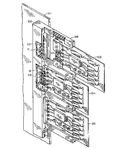
Referring now to FIG. 1, a typical ~olid-state line
frame in accordance with the present invention include~ a
plurality of ~iles o~ 2~-1/2 " high motherboards 101 as
shown in part in FIG. 1. In the anticipated arrangement,
each file would contain 32 motherboards on 1" centerlines.
Each motherboard has two columns of 12 line card~ located at
the front edge. A~ may be seen in FIG. 1, three line cards
only have been shown for purposes of clarification. These
; are numbered 103, 104 and 105, re~pectively. In accordance
with the present embodiment, each line card is approxi~nately
1-1/2" wide by 3-1/2" long. The line cards are plugged into
a two-piece dual bodied connector 102 located at the front
end of motherhoard 101. It is this connector 102 shown in
multiple form that becomes the basis o-f' the present
invention.
As may be seen by ref'ererlce to FIa. 1, the individllal
line cards, such a~ 103, 104 and 105, are inserted into the
line card connector 102 with the help of card guides 106,
107, 108 and 109 which extend Ollt f'rom the face of' connector
102. These card guides also help to support the :line cards
26 af`ter they are in~erted. The principal intent of the
~2~ 83-4-l37
present invention is to provide mean~ whereby the cards
may be preven-ted from "walking" out in response to vibration.
Ina~much as the total mas~ of each of the individual
line cards 103, 104, 105, etc. are fairly small, it can be
6 determined that if a ~light amount of card retainin~ force
could be incorporated into each individual contact included
with each of the line cards, the approximately 22 contact~
associated with each line card would generate more than the
amount of retaining force reguired to maintain the plugged
connection for each line card. For purpose~ of
clarification, a substantially fewer number of contacts have
been shown in the drawing, such as the contacts 111 and 112
~hown in the connector portion and contac-ts 117 and 118
shown attachsd to the line cards themselve~. A number of
different coDtact arrangements have been shown and will be
described in detail at this point.
Referring first to FIas. 2A, 2B and 2C, the molded
housing~, ~uch as 102, are not shown for purposes o~ clarity
~ince they do not represent any particular new technology.
The contacts shown in FIa~. 2A, 2R and 2C are flat material
contacts of a spring con~truction as conventionally used for
contacts and i~ ~uggested being bent in accordance with the
configuration ~hown. Referring again to FIG. 2A, movable
contact 201 and the fixed contact 202 are shown in cro~s
section prior to mating. Each of the contacts, as may bs
0een in FIG. 3, have an embossed area having a concave or
83~ 137
convex depression in the blade portion of each contact. The
flat blade portions of each contact are separated by a
distance shown a~ D . The embossed portion or depres~ed
concave section o-~ the movable contact 201 has a leading
angle A aDd a trailing angle B relative to the -flat blade
portion of the contact. The leading angle A control~ the
insertioD force and the trailing angle B controls the
extraction f`orce of the contact system. As may be seen in
FIC. 2B during mating, the movable and fixed contacts are
caused to flex and separate due to the embossed or depressed
portion on the movable contact. When the contact~ are fully
mated, as ~een in FIG. 2C, the depressed or embossed portion
of the movable contact is ne0ted in the embo~0ed or
depressed portion of the fixed contact and the blade portion
of both contact0 are ~eparated by distance D . As may be
seen by reference to FIGs. 2A and 2C, the distance D i9
greater than D which means both springs are ~till in a
deflected position relative to their free states. I-f a line
card, which :i9 equipped with a substantiRl number (0uch a~
22 in the present embodiment) o~ movable contacts, starts to
vibrate or "walk" out of its plugged position, the ne~ted
embo~ses or depre~ions would force the contact blades apart
and di~tance D would have to lncrea0e. However, the
contact ~orce~ would al~o have to increase which in turn
will then tend to maintain the two embosses or depresse~ in
the ne~ted po~itio~. Thu~, in effect, the electrical
~ 83-~-137
contacts are also ths mechanical means by which each
iDd-lvidual line card is maintained in its proper plugged
po~ition. In practice, these retention forces would be made
large enough to prevent the line cards from "walking", but
low enough to keep card extraction forces reasonable when a
line card is purposely withdrawn as may be required for
maintenance or other purpose~.
Referring now to FIG. 3, blade contacts are ~hown
employing circular embosses or depression~ as described in
connection with FIGs. 2A, 2B and 2C. As in FIGs. 2A, 2B and
2C, the leading edges o~ the blade~ of each set or pair of
contacts have been curved so as to prevent stubbing of the
blade contacts during initial engagement. As may be seen in
FIG. 3, the movable contact 301 includes a depression or
dimpled area 303, while the ~tiff or fixed contact 302
includes a ~imilar depre3~ion 304.
Referring now to FI~. 4, similar principle~ are
discussed. The combination ~hown in FI~. 4 consists of a
movable spring contact 401 including a ~lot 403 therein and
a rigid or stlf~ contact 402 having a forward projecting
ramp 404 and a rearward ~acing ramp 406. The combina-tion of
the contacts of FIa. 4, like tho~e in FIa. 3, is similar and
; follow~ the same general form of operation during mating as
de~cribed in connection with the di~cussion of FIas. 2A, 2B
~25 and 2C. Durin~ actual engagement, however, of the contact~
;of FIG. 4, the ramp portion con~i~ting of the forward and
~L2~7~S8
83-4-137
rearward ~acing ramps 404 and 405 glides across the ~pring
contac-t 401 and engages slot 403, the juncture portion of
contact 402 being where ramps 40~ and 405 mee-t.
Referring again to FIG. l, it can be seen how card 103
is yet to be inserted when pu3hed in a ~orward direction.
While being maintained in position by guides 106 and 107,
the contacts 117, which are retained in the part of the
connector known as 116, will advance forward to engage the
re~ilient or flexible contact~ 113 which will engage and
retain both electrical and mechanical contact.
Al~o, a~ may be ~een in FI~. l, card 104 has been
inserted so that the rigid contact~, such a~ 118, are now
engaging the contacts ~uch as ll~. It can also be ~een here
that contacts, ~uch as 113 and 1l4, are a portion of the
connector 102 affixed to the motherboard 101 while the
contacts, ~uch as 117 and 118, are included in that portion
o~ the connector known as 116.
It will be obvious to those skilled in the art that
numerous modi~ication~ o~ the present invention may be made
2() without departlng from the splrit of the invention which
~hall be limited only by the scope of the claim~ appended
hereto.