Note: Descriptions are shown in the official language in which they were submitted.
HIGH PERFORMANCE LOW PIN COUNT BUS INTERPACE
BACKGROUND OF THE INVENTION
The present invention relates to the field of com-
puter data buses generally and more specifically to high speed
buses which allow bidirectional communication. In most buses,
especially buses that contain multiple lines to transfer data
in a parallel format, there are windows of time during which
data on the bus is valid. In synchronous buses, periodically
repeating cycles form the basis for timing of such buses and in
each of those cycles windows are usually defined by a separate
signal which becomes active once per bus cycle. During the
time between windows, the data on the bus is allowed to change
to new levels and is considered to be invalid.
In general, data communication on a bus involves a
bus driver to place data onto the bus and a storage device to
retrieve and store data from the bus. The bus driver, can gen-
erally be one of two types. One type can only drive a bus line
to one level, e.g., to a ground potential, and thus requires a
pull-up or precharging de~vice to establish the other bus level.
The other type actively ~i~e the bus line to both levels and
does not require precharging or pull-up devices. When a drive
signal controlling the bus driver is in one state, it enables
the bus driver and causes the bus driver to drive the bus to a
level (either the same or inverted) corresponding to input data
at the input terminal of the bus driver. When the drive signal
is in the other state, it disables the bus driver causing the
bus driver to cease driving the bus. Immediately following the
enabling of the bus driver, while the data on the bus i9 still
changing, the data is also considered to be invalid. For each
particular driver technology and intexface characteristics,
this data invalld time is relatively fixed, as it depends on
conditions like bus length, bus driver propagation delay, etc.
As bus frequencies increase, the cycle times of the bus
decreases, and the bus driver enable time decreases correspond-
ingly. Thus, the amount of the bus dxiver enable time during
which data is valid also decreases.
!`
7~
The storage device responds to the actuation of a
latch signal by storing the data currently on the bus. The
latch signal must be timed so that the storage device stores
data while it is still valid on the bus, and conventional prac-
tice is to time the latch signal so that the storage device
stores data while the bus driver is still enabled. ~hus the
conventional drive signal continues to drive the bus for some
"hold time" after the latch signal is actuated. Conventional
practice for driving buses between sets of integrated circuit
chips is to actuate the latch prior to disabling the bus driver
because the voltage levels on the bus may be indeterminate when
the bus is not being driven, and during such times the storage
device may not actually store the data intended to be trans-
ferred over the bus from the bus driver.
Generation of the bus driver and latch signals to
obtain the hold time re~uires two separate clock signals: one
for the latch signal and one for the drive signal which extends
beyond the latch signal. Those two clock signals, however, are
only sufficient for unidirectional communication on the bus
lines. Full bidirectional communication on the same bus lines
requires two storage device/bus driver pairs, as well as four
clock signals (two signals for each direction).
Furthermore, the drive signal used for communication
in one direction on the bus must not overlap the drive signal
used for communication in the other direction so that the bus
drivers used for communication in each direction are not driv-
ing the bus simultaneously. If they do drive the bus simulta-
neously even for only a small amount of time because of clock
skew, for example, then the drivers and the bus lines will
experience current spikes, and the availability of the data
transferred by the second drive si~nal will be delayed.
The generation of the multiple clocks for
bidirectional communicatioll is further complicated if that com-
munication must be synchronized to an overall system clock.
For example, if there we e a system bus with its own bus ti:ing
coupled to one of the elements of the bus, then the four clock
signals necessary ~or bidirectional communication ~ould have to
be synchronized with the timing of l:his system bus. Such
7g~L
synchronization may be difficult for several reasons. First,
the cycle time of the clock used for the system bus may be so
smalL as~to make it impractical to further subdivide the clock
cycle time to o~tain four different clock signals conforming to
the reqùirements for bidirectional communication, Furthermore,
even if it were possible to obtain those clock signals, their
pùlse widths may be so narrow that logic circuitry in the ele-
ments could not reliably respond to them.
One design approach would be to eliminate t'ne need
for the four separate clock signals by using two unidirectional
buses, one for communication in each direction. The addition
of another set of lines for the other unidirectional bus, how-
ever, doubles both the number of bus lines and the area which
must be dedicated for those lines. In addition, the use of
such buses doubles the number of pins on the components which
couple to that bùs. Thus, for example, to transfer 6~ bits of
data in parallel using two unidirectional buses would require
an additional 64 pins per interface as compared to a single
bi~irectional bus.
Of all these disadvantages, the increased pin count
may be the most severe. If the number of pins required exceeds
the number that can be supported in a single integrated chip,
then multiple chips must be used for the circuitry, This can
be disadvantageous because circuitry generally operates more
slowly when divided between multiple chips, Thus, the design
of high speed circuitry frequently involves the development of
techniques that minimize the required number of pins to avoid
dividing functions across chip boundaries, Pin counts are
often a limiting factor in circuit design because of limited
space for those pins on printed circuit boards,
Another desirable design goal for a high speed bus
interface between two buses, such as a dedicated user bus and a
main system bus, is to place on the user bus a copy of all the
communications on the main system bus. This allows circuitry
coupled to the user bus to monitor the use of different re-
sources on the main system bus. To meet this requirement, data
must be transferred from the system bus to the user bus during
each cycle of the system bus. If the user bus uses single
- ~ -
lines for bidirectional communication, then that bus must oper-
ate twice as fast as the system bus to allow two communications
(one each direction) during each cycle of the system bus
cycles. This requirement further exacerbates the timing prob-
lems.
If the user bus can be synchronized with the system
bus and reproduce the traffic on tile system bus, including mes-
sages placed on the system bus frorn the user bus, several
advantages are available. One advantage of this system is that
one user of the system bus can monitor the system bus transac-
tions of all the other users. For example, one user can ensure
that its cache memories are valid by checking all the memory
write operations of the other users. Users can observe their
own system bus transactions in relationship to the system bus~
transactions of other users. In addition, users can send mes-
sages to themselves over the system bus to permit easy
coordination of node resources, such as system bus control and
status registers, that are accessible over the sytem bus.
Accordingly, it is an object of the present invention
to minimize the number of clock signals needed for high speed
bidirectional bus transfer without driver overlap.
Another object of the present invention is to provide
high speed data transfer between two buses so that one bus can
obtain a copy of all traffic on another bus.
Yet another object of the invention is to provide one
bus with a return copy of the messages it sent to tne other
bus.
A still further object of the invention is to mini-
mize the number of pins needed for an interface to a high speed
sy~stem bus.
AdditionaL objects and advantages of the invention
will be set forth in ~art in the description which follows, and
in part will be obvious f~om the description, or may be ledrned
by practice of the invention. The objects and advantages of
the invention may be re~lized and obtained by the instrumen-
talities and combinations particularly pointed out in the
appended claims.
~z~
-5--
SUMMARY OF THE I I`IVENT r ON
The present invention overcomes the problems and dis-
advantages of the prior art by providing bidirectional transfer
between pin terminals by carefully controlling the timing of
the transfers in each direction.
To achieve the objects and in accordance with the
pùrpose of the invention, as embodied and broadly described
herein, an interface system of this invention provides
bidirectional communication for a node and a system bùs
propagating data during repetitive bus cycles, the node having
a user portion for processing the data. The interface system
comprises: a node bus, coupled to the user portion, for trans-
ferring the data in parallel; transceiver means, coupled
between the node bus and the system bus, for providing
bidirectional communication between the system bus and the node
bus and for providlng to the node bus a copy of all of the data
propagated on said system bus and timing means. The
transceiver means includes first unidirectional communications
means, responsive to active portions of a first clock signal
occurring once each system bus cycle and having input terminals
coupled to the node bus and output terminals coupled to the
s~stem bus, for receiving data from the node bus for later
transfer to the system bus during selected cycles of the system
bus, and second unidirectional communication means, responsive
to active portions of a second clock signal occurring once each
system bus cycle and having input ter~minals coupled to the sys-
~-.l tem bus and output terminals coupled'the node bus for trans-
ferring the data propagated on the system bus to the node bus
once every cycle of the system bus, each of the input terminals
being connected to a differerlt one of the output terminals of
the first unidirectional cornmunications means and each of the
output terminals being conr.ected to a different one of the
input terminals of the first unidirectional communications
means. The timing means is coupled to .he first and secand
unidirectional co~munication means and provides the first and
second clock signals so that the active portions of the first
and second clock signals do not occur simultaneously and so
that the active portions of the second clock signal~ cause the
99~
-6-
-
second unidirectional communication means to return to the node
bus a copy of the data trans~erred to the system bus from the
node bus.
The accompanying drawings, which are incorporated in
and constitute a part oE this specification, illustrate an
embodiment of the invention and together with the description
serve to explain the principles of the invention.
I I I . ~RIEF D~.SCRIPTION OF THE DRAWINGS
F~ig. 1 is a block diagram of a data processing system
including a system bus using the present invention;
Fig. 2 is a block diagram of a node in the data pro-
cessing system of Fig. 1:
Fig. 3 is a timing diagram showing timing signals
used in the data processing system of Fig. l;
Fig. 4 is a block diagram of the data interface in
the node of Fig. 2;
Fig. 5 is a block diagram of the arbiter in the data
processing system of Fig. l;
Fig. 6 is a detailed block diagrarn of the data inter-
face in Fig. 2 and of interface circuitry for the node bùs in
Fig. 2;
Fig. 7 is a block diagram of portions of clock
decoder 63 shown in Fig. 2;
Fig. 8 shows a CMOS output circuit,~
Fig. 9 shows a CMOS input curcuit; and
Fig. 10 shows timing si~nals for the node bus 67
shown in Fig. 2.
IV. DETAILED D~SCR~PTION OF THE PREFERRED EMBOD r MENT
Reeerence will now be made in detail to a preferred
embodiment of the invention, an example of which is illustrated
in the accompanying drawings.
. System Overview
Fig. 1 shows an example of a data processing system
20 which embodies the present invention. rhe heart of system
20 is a system bus 25 which is a synchronous bus that allo~s
communication between several processors, memory subsystems,
and ~/O systems. Communications o~er system bus 25 occur syn-
chronously using periodic bus cycles. A typical bus cycle time
for system bus 25 is 6~ nsec.
..
!
66~22-55
ln Fiy. 1, system bus 25 is coupled to ~wo processors
3:L and 35, a m~mory 39, one I/0 interface 41 and one I/0 unit
51. I/0 unit 53, is coupled to system bus 25 by way oi` I/0 bus
4 and I/0 unit in~erface ~l.
A cenkraL arbiter 28 is also connected to system bus
25 in the pret`e~red embodinlent of data processing sys~em 20.
Arbiter 28 provi.des certa:in timing and bus arbitration siynals
directly to the other devices on system bus 25 and shares some
signals with those devices.
The implementation shown in Fig. 1 is one which is
presently preferred and shollltl not necessarily be interpreted
as limiting the present invention. For example, I/0 unit 53
could be coupled directly to system bus 25, and arbiter 28 need
not operate in the manner clescribed for the present invention.
In the nomenclature used to de.scribe the presenk
invention, processors 31 and 35, memory 3gr and I/0 interface
41, and I/0 device 51 are all called nodes. A "node" is
de.fined as a hardware device which connects to system bus 25.
A typical node 60 is .shown in greater detail in Fig. 2.
Accordiny to the nomenclature used to describe the
present invention, the terms "siynals" or "lines" are mainly
used interchangeably to refer to the names of the physical
wires. The -terms "data" or "levels" are mainly used to re:~er
to the values which the signals or llnes can assume.
Nodes perform transfers with other nodes over system
bus 25. A "transfer" ls one or more conticJUouS cycles that
share a common transmitter and common arbitration. Eor
example, a read operation i.nitiated by one node to obtain
in:Eormation ~rom another nocle on system bus 25 requires a
commancl transfer from the first to the second node fo:Llowed by
one or more return data transfers from the second node to the
first nocle at some later tlme.
A "transacti.on" is deilned as the complete logical
task heiny performed on system bus 25 and can include more than
one transfer. For e~ample, a read operation consisting of a
command transfer followed later by one or more return data
transfers is one transaction. In the p:referred embodiment of
system bus 25, the permi.ssible transactions support the
transfer of different clata :Lengths and include read, write
(masked),
,
~` 7
~L2~
interlock read, unloek write, and interrupt operations. The
difference between an interlock read and a regular or
noninter~ock read is that an interlock read to a specific loca-
tion retrieves in~or~ation stored at that location and re-
stricts access to the stor-ed information by subsequent
interlock read commands. Access restriction is performed by
setting a lock mechanism. A subse~uent unlock write command
stores information in the specified location and restores
access to the stored information by resetting the lock mecha-
nism at that location. Thus, the interlock read/unlock write
operations are a form of read-modify-write operation.
Since system bus 25 is a "pended" bus, it fosters
efficient use of bus resources by allowing other nodes to use
bus cycles which otherwise would have been wasted waiting for~
responses. In a pended bus, after one node initiates a trans-
action, other nodes can have access to the bus before that
transaction is complete. Thus, the node initiating that trans-
action does not tie up the bus for the entire transaction time.
This contrasts with a non-pended bus in which the bus is tied
up for an entire transaction. For example in system bus 25,
after a node initiates a read transaction and makes a command
transfer, the node to which that command transfer is directed
may not be able to return the requested data immediately.
Cycles on bus 25 would then be available between the command
transfer and the return data transfer of the read transaction.
System bus 25 allows other nodes to use those cycles.
In using system bus 25, each of the nodes can assume
different roles in order to effect the transfer of information.
one o those roles is a "commander" which is defined as a node
which has initiated a transaction currently in progress. For
example, in a write or read operation, the commander is the
node that requested the write or read operation; it is not nec-
essarily the node that sends or receives the data. In the pre-
ferred protocol for system bus 25, a node remains as the com-
mander throuyhout an entire transaction even though another
node may take ownership of the system bus 25 during certain
cycles of the transaction, For example, although one node has
control of system bus 25 during the transfer of data in
66~22~55
respon~e ~o ~he cornmand transfer of a read transac-tion, that
one nocle does not become the commander of the bus 25. :Lnsteacl,
this node is ca:llecl a ".responder."
A r~sponder responds ~o the commander. ~or example,
i~ a commander ini-~iated a write operation to write data from
l~ode A to nocle B, node B woulcl be the responder. In addi~.ion,
in data processing sys~em 20 a node can simultaneously be a
commander and a responder.
Transmitters and receivers are roles which the nodes
assume in an indi~idual transfer. A "transmitter" is defined
as a node which is the source of information placed on system
bus 25 during a transfer. A "receiver" is khe complement of
the transmitter and ls defined as the nocle which receives the
information placed on system bus 25 during a transfer. During a
read transaction, ~or example r a commander can first be a
transmi-tter duriny the command transfer and then a receiver
duriny the re-turn clata transfer.
When a node connected to syste~ bus 25 desires to
become a transmitter on system bus 25, that node asserts one of
two request linesr CMD REQ (c:ommander request) and RES RE,Q
(responcler request) r which are connected between central
arbiter 28 and that part:Lcular node. The CMD REQ lines are
shown generally in Fig. 1. In general r a node uses its CMD REQ
line to request to become commander and in:itiate transactions
on ,system bus 25r and a node uses Its RES REQ line to bec!ome a
:responder to return data or message to a commancler. Generallyr
central arbiter 28 detect;s which nodes desire access to the bllS
(i.e. r which request line~ are asserted). The arbi~er then
responcls to one of the asserted request l:Lnes to grant the
correspondlny node acces.s to bus 2S accord:LncJ to a priorlty
algorlthm. :Ln the preferred embocl:Lmerlt, arbiter 28 ma:Lntains
two inclependent, clrcular queuesl one for the commander
reques~s and one for the responcler request.s. Preferablyr the
responcler requests have a higher priority than the commander
requests ancl are hanclled befGre the commander requests.
The commancler request lines and responder request
lines are consiclerecl to be arbitration signals. As illustratecl
in Fig. 1, and as will be explained in greater detail in the
description of Fig. 6, arbitration signals also include point-
to-point conditional grant signals from central arbiter 28 to
each node, system bus extend signals to implement multi-bus
cycle transfersr and system bus suppression signals to control
. 9
,~ .
79~
66822-55
t~e inltiation of new bus transactions when, for example, a
node such as memory is momentarily unab].e to keep up w:Lth
traffic on the sys-tem bus.
Other types of signals whi~h can constitute system
bus 25 inalude information transfer signals, respond signals,
control s~gnals, console/f.ront panel signals, and ~ few
miscellaneous siynals. Infor~ation transfer signals include
data signals, func~ion signals which represen~ the function
being performed on the system bus 25 during a current cycle,
identifier signals identifying the commander, and parity
signals. The respond signals generally include acknowledge or
confirmation signals from a receiver to notify the transmitter
of the status of tha data transEer.
Control signals include clock signals, warning
signals, such as those identifying low line voltages or low DC
voltayes, reset signals used during initialization, node
failure signals, default signals used durlng idle bus cycles,
and error default siynals. The console~front panel signals
include siynals to transmit and receive serial data to a system
console, boot siynals to control the behavior o~ a boot
proaessor during power-up, signals to enable modlfication of
the erasable PRO~ of proaessors 31, 35 on system bus 25, a
signal to aontrol a RUN LIGHT on the front panel, and signals
providing batter~ power to clock logic on certain nodes. The
miscellaneous siynals, in addltion to spare signals, include
ident:Lflcation signals which allow each node to define its
identification code.
Fig. 2 shows an example of a node 60 connected to
system bus 25. Node 60 could be a processor, a memory, an I/O
unit or an :t/O lnterface as shown in l'ig. 1. In the example
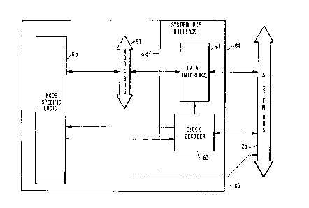
shown in ~ig. 2, node 60 lncludes node ~peclfic logic 65, a
node bu~ 67, and a system bus interface 64 contalnlng a data
lnterface 61 and a clock decoder 63. Preferably, data
lnterface 61, alock decoder 63, and node bus 67 are standard
elements for nodes aonnec~ed ~o system bus 25. The node
speciflc logic 65, which uses different lntegrated circuits
from system bus lnterface 64r preferably includes, in addition
to the circul~ry designed by a user to carry out the specific
funation of a node, standard circultry to interface with the
node bus 67. Xn yeneral, data interface 61 is the primary
logical and electrical in~erface between node 60 and system bus
25, clock decodar 63 provldes timing signals to node 60 based
lZ~-3~ 66822-55
on eentrally generatecl eloeh signalsr and nocle bus 67 provicles
a high speed in-terfaee between data interfaee 61 ancl node
spec~ific logie 65.
In ~he preferred embodiment o~ nocle 60 and syst~ln bus
interfaoe 64 shown in fig. 2, elock decoder 63 eontains eontrol
eireuitry for forming signals to be plaeed on system bus 25 and
proeesses elock signals re~ei~ecl from eentral arbiter 28 to
obtain timing s1gnals for node speeifie :Logie 65 and data
interface 61. Sinee the ~iming signals obtained by cloek
cleeocler 63 use the centrally generated eloek signaLs, node 60
will operate synchronously with system bus 25.
Flg. 3 is a timing diagram showiny one bus cycle, the
clock signals received by clock deeoder 63 from eentral arbiter
28 (Fig. 1), and certain of the timing signals generated by
elock deeoder 63. The cloek signals received by eloek deeocler
63 include a 'rime H signal, a Time L signal, and a Phase signcll
as shown in FicJ. 3. Time H and Time L are inverses of the
~undamental c:loek signals and the Phase signal is obtained by
dividing the fundamen~al eloek signal by three. The timing
siynals generated by c~loell deeoder 63 inelude C12, C23, C3~,
C45, C56 and C61, all of whieh are shown in Fig. 3. Those
timing signals requlred by clata interfaee 61, whieh oeeur onee
per bus eyele, are providecl to data interfaee 61, and a
eomple~,e set of timiny sig~al,s, ine:luding equivalent ones of
the timing slgnals provided to data interfaee 61, is buf~ered
and provldecl to the node speei~ie logie 65, The purpose of
buffering is to insure that node speei~ic logie 65 eannot
adversely affect the operation of the system bus interfaee 64
by improperly loading the t:Lming signaLs. Cloek deeocler 63
uses the eloek ;lgnalæ to ereate six .subeyeles for eaeh bus
eyele and -then uses the suheyeles to ereate the six timlng
signals CXY, where X and Y represent two ad~aeent subeyeles
whieh are eombined to form one tirne signal,
Eaeh node in the system bus 25 has its own
eorresponcling set of timing signals generated by its eloek
deeoder 63. While
11
-i~
~L2i~
nominally the corresponding signals occur at exactly the same
time in every node throughout the system' variations between
clock deçoder 63 and other circuitry in multiple nodes intro-
duce timing variations bet~een correspondinq signals. These
timing variations are commonly known as "clock skew."
Fig. 4 shows a preferred embodiment of data interface
~1. Data interface 61 contains both temporary storage cir-
cuitry and bus driver circuitry to provide a bidirectional and
high spee interface bet~een each of the lines of node bus 67
and each of the lines oE system bus 25. As shown in ~ig. ~,
data interface 61 preferably includes storage elements 70 and
72 and system bus driver 74 to provide a communication path
from node bus ~7 to system bus 25. Data interface 61 also in-
cludes storage element 80 and node bus driver 82 to provide
comrnunication path from system bus 25 to node bus 67. As used
in the description of data interface 61, the term "storage ele-
ment" refers generally to bistable storage devices such as a
transparent latch or a master-slave storage element, and not to
a specific implementation. Persons of ordinary skill will rec-
ognize which types of storage elements are appropriate.
As shown in Fig. 4, storage element 70 has an input
connected to receive data from node bus 67 and an output con-
nected to the input of storage element 72. The output of stor-
age element 72 is connected to an input of system bus driver 74
~hose output is connected to system bus 25. Storage elements
70 and 72 are controlled by node bus control signals 76 and 78,
respectively, which are derived from the timing si~nals gener-
ated by clock decoder 63. Storage elements 70 and 72 prcvide a
two-stage temporary storage ~or pipelining data from node bus
67 to systern bus 25. Different numbers of storage stages can
also be used.
System bus driver 7~ is controlled by system bus
drive~ enable 79. According to the state of th: system bus
drive~ enable 79, the input of system bus driver 74 either is
coupled to its output, thereby transferring the data at the
output of storage element 72 to system bus 25, or decoupled
from that output. When system bus drive enable 79 decouples
the input and output of the system bus driver 7~, system bus
7~
-13- 66822-55
driver 74 presents a high impedance to system bus 25. The sys-
tem bus drive enable 79 is also generated by clock decoder 63 in
accordance with clock signals received from system bus 25 and
control signals received from the node spècific logic 65.
Storage element 80 has an input terminal connected to
system bus 25 and an output terminal connected to an input of
node bus driver 82. The output of node bus driver 82 is connec-
ted back to node bus 67. Storage element 80, preferably a
transparen-t latch, is controlled by a system bus control signal
85 which is derived from the timing signals generated by clock
decoder 63. A node bus drive signal 87 controls node bus driver
82 similar to the manner in which system bus drive signal 79
controls system bus driver 74. Thus, in response to node bus
drive signal 87, node bus driver 82 either couples its input to
its output or decouples its input from its output and provides a
high impedance to node bus 67.
In order to explain how data is transferred over sys-
tem bus 25, it is important to understand the relationship
between system bus drive enable 79 and control signa.l 85. In
this present embodiment, this relationship is shown in Fig. 3.
System bus drive enable 79 is nominally driven from the begin-
ning to the end of a bus cycle. The new data become available
for receipt from system bus 25 at some time later in the bus
cycle after driver propagation and bus settling time has occur-
red. In the present embodiment, storage element 80 is a trans-
parent latch. Control signal 85 is logically equivalent to
clock C45. The bus timing assures that system bus 25 data is
available for receipt some time prior to the deassertion of con-
trol signal 85. Storage element 80 stores bus data that is
,,,I,~r
~z~
~ 66822-55
stable at least a set-up time prior to the deassertion of con-
trol signal 85 and remains s-table a hold time a-Eter -the deasser-
tion of control signal 85.
Node bus 67 is preferably a very high speed data bus
which allows bidirectional data transfer between the node speci-
fic logic 65 and system bus 25 by way of da-ta interface 61. In
the preferred embodiment of node 60 shown in Fig. 2, node bus 67
is an interconnect system consisting of point-to-point connec-
tions between the system bus interface 64 and -the node specific
logic 65. In accordance with the present invention, however,
there is no requirement for such point-to-point interconnection.
Fig. 5 shows a preferred embodiment of the central
arbiter 28 which is also connected to system bus 250 Central
arbiter 28 provides the clock signals for system bus 25 and
grants ownership of the bus to the nodes on system bus 25 owner-
ship of that bus. Central arbiter 28 preferably includes an
arbitration circuit 90, a clock circuit 95, and an oscilLator
97. Oscillator 97 generates the fundamental clock signals.
Clock 95 provides timing signals or arbitration circuit 90 and
the basic Time H, Time L, and Phase clock signals for timing on
system bus 25. Arbitration circuit 90 receives the commander
and responder request signals, arbitrates conflicts between
nodes desiring access to system bus 25, and maintains the queues
referred to above for the commander and responder requests.
Arbitration circuit 90 also provides certain control signals to
clock 95.
B. Bus Interface Circuitry
In node 60, as shown in Figs. 2 and 4, each data
interface 61 is coupled to a corresponding line of system bus 25
~r
- ~2~
- 14a - 66822-55
by a single pin terminal. The connection can be direct but is
preferably through a resis-tance for reasons not relevan-t to an
understanding of the present invention. For the reasons ex-
plained in the Background of the Invention, it is desirable that
each data interface 61 also be coupled by a single pin terminal
to a corresponding line of node bus 67 for those lines of node
bus 67 which correspond to the lines of system bus 25. By using
single pin terminals, node bus 67 can be a single bidirectional
bus instead of two parallel buses, and the number of pins or
terminals needed is thus minimized. In addition, the circuitry
connected to node bus 67 need not be divided among several inte-
grated circuit chips only to satisfy increased pin count needed
to interface to two parallel buses.
In addition, for -the reasons explained in the Back-
ground of the Invention, the design of circuitry to accomplish a
single pin terminal to single pin terminal, bidirec-tional trans-
fer is complicated by the desire to place on node
.,~,,~
bus 67 a copy of all the data or messages from system bus 25,
including the data on system bus 25 provided by node 60. Doing
~o allows the node specific logic 65 to view all the data or
messages on system bus 25 which in turn helps to manage systern
bus 25. By ~aking available to node specific logic 6~ all the
data or messages on system bus 25, node 60 can use the knowl-
edge of which resources of data processing system 20 are being
used and by whom those processes are being used to implement
certain self-management techniques for use of system bus 25.
In addition, the provision of bidirectional communi-
cations between data interface 61 and system bus 25 through a
single pin terminal for each line of system bus 25 allows ~ode
specific logic 65 to monitor and receive its own messages to
system bus 25. Such connection also allows node specific logic
65 to send a message to itself by way of system bus 25 so other
nodes can monitor those transactions.
Another benefit of cycle by cycle visibility of sys-
tem bus 25 to node bus 67 is to maintain cache coherency. With
regard to this use, if a node moclifies the contents at memory
locations accessible through system bus 25, the other nodes can
monitor such accesses and determine whether their own caches
include copies of these memory locations.
To provide single pin terminal connection as well as
bidirectional transfer capability during each cycle of system
bus 25, node bus 67 must operate at twice the speed of system
bus 25, as explained in the Background of Invention. Node bus
67 must therefore have shorter transfer times than system bus
25.
In the preferred embodiment of the invention, with a
64 nanosecond cycle time for system bus 25, only six subcycles
ar~ available due to the requirements of circuitry in, for
e.Yample, system bus inter-face 64 ~hich is composed of C~OS cir-
cuitry. Six timing signals, C12, C23, C34, C45, C56, and C61,
each covering two subc~cles, are formed for timing of node bus
67.
In the conventional method of bidirectional bus
transfer requiring t~o pairs of cloc~ signals, the timing nec-
essary to form those signals is dif icult to implement using
~2~
-16-
the timing siqnals in Fiq. 3 or any other signals based on the
six subcycles. In fact, the implementation would only be pos-
sible by creating special timing signals for drivers which were
longer than the timing signals shown in Fig. 3 (e.g., a three-
subcycle long signal such as C123) or by creating latch control
signals shorter than those timing signals (e.g., a single
subcycle signal such as Cl or C2). In the first case, a high
probability exists that two different drivers would drive the
bus at the same time since the longer clock signals (e.g., C123
and C456) would need to be used to control the drivers and
clock skew may cause those signals to overlap and drive the bus
at the same time. In the second case, the shorter timing sig-
nals may not be long enough to be used effectively by the logic
circuitry or to permit the data to propagate from the driver t~
the latch prior to actuation of the latch. Thus, a conven-
tional bus driving method requires timing signals which may be
obtained from a minimum of eight subcycles. This would allow
two three-subcycle driver signals, separated by one subcycle to
prevent overlap, and the latch control signals could lasts for
the first two of the three-subcycle drive signals.
The present circuit avoids problems of bidirectional
data transfer when there is a limited number of subcycles and
other circuit constraints by using a phenomenon of bus lines
which has not been previously exploited for the problem of data
transfer across integrated chip boundaries. Each of the lines
of node bus 67 has an inherent capacitance of typically 5 10
pf, The inventors have found that this inherent capacitance
can be used to maintain the proper voltage levels on the bus
lines even after the bus is no longer being actively driven to
a particular level by a bus driver. To store charge in the bus
line inherent capacitance, the impedance of the discharge paths
of that capacitance must be high. In general, the discharge
paths for a bus are through che driver outputs and storage ele-
ment inputs connected to that bus. The inventors have ound
that by using devices ~ith high input and output imp~ances,
speci~ically CMOS devices ~hich also add several picofarads of
cap~citance to the bus lines, tne inherent capacitance of the
bus lines can be used to e.Ytend tne time during ~hich the data
7~
66822-55
placed in the bus is valid even after the drlve signals are
removed from the bus drivers.
The interface apparatus comprises a plurali.ty of bus
drivers each corresponding to a cli~ferent llne of the bus.
Each of the drivers is capable oi driving the corresponding bus
line to either o~ two voltage levels. Fig. 6 shows an example
of one line of bus 67 connected to circuitry in node specific
logic 65 and in data interface 61. Bus driver 82, which has
already been described, is shown as being coupled to that line
o~ bus 67. Bus driver 82 includes an input terminal 91 for
holding input data to be transmitted to the line of node bus 67
from storage element or latch 80, and a bus interface terminal
92 which is actually coupled to the line of node bus 67. Bus
driver 82 also has an enable terminal 94 which receives a two-
state drive signal, callecl DRIVE 87 in Fiy. 4 and shown
specifically as C61 in Fig. 6.
Fig. 3 shows the timing of signal C61. When C61 is
high ~the designation of levels is a convention and not a
requirement), the output terminal 92 drives the corresponding
line of node bus 67 to one of the levels according to the input
data. When signal C61 is low, then the bus driver 82 ceases
drlving the bus line and presents to the line of node bus 67 a
high impedance.
The interface apparatus also includes a plurality of
latches each corresponding to a dif~erent line of the bus. As
Fig. 6 shows, a storaye element or latch 110 is coupled to the
same line Orc nocle bus 67 as is clriver 32. Storage element or
latch 110 hai~ an input tertninal 112 coupled ko that line of
node bus 67 and presqnts a high lmpedance to that line.
Storaye element 110 al50 has a control terminal 114 for
receivlncJ a control signal which, as shown ln Eig. 6, is also
C61. The control signal at terminal 11~ causes storage element
110 to store the level on the corresponding line of node bus 67
when that control siynal is actuated (i.e., when C61
deasserts). In general, a control signal is actuated during a
single transition between states, such as either a rising or a
falliny edge, but not both.
The interface apparatus aliso includes signal
generatlng means coupled to the plurality of latches to
generate drive and control signals to transfer the input data
at the input terminals o~ the bus drivers through the bus to
the latches as embodiecl herein. Fig. 7 shows an example of
17
~ ~J~
6G822-55
clock decoder 63 including circuitry to derive control sicJnals
such as signal C61. In Eig. 7, the Time L siclnaL is received
through buffer 13~ and coupled ~o a cloc}c input of a three bi~
shift register 132. The PHASE signal after passing thro~yh
buffer 134, is provided to the data input terminal of shift
register 132. The Q1, Q~, and Q3 outputs of that register are
passed through buffers 140, 138 and 136, respectively, to form
the C12, C3~, ancl C56 signals, respectively. ~he Q1 outpu~ of
shift register 132 provides the data input to a three-bit shift
register 142 whose clock input is coupled, through buffer 144,
to the TIME H signal. The Q1, Q2, and Q3 outputs of register
142 are passed through buffers 150, 148, and l~G to form the
C23r C~S, and C61 signals, respectively. As Fig. 3 shows, the
active por-tion of clock signal C'61 in the preferred embodiment
lasts for about one-third of the cycle of system bus 25.
The s:Lgnal generatiny means inclucles first means fo:r
switchiny the drive signals from the first state to the second
state at substantially the same time as the corresponding
control signals are actuated. In other words, the drive siynal
need not remain an adclitional subcycle after the latch signal.
In the preferred embodiment, clock decoder 63 generates timing
signal C61 ior bo~.h the driver and control signals. As
explained prevlously, it is preferable to isolate the timing
signal C61 which ls sent -to data interface 61 from the timing
sLgnal C61 which ls sent to node specific logic 65 and thus
storage element or latch llO. Both timing signals, however,
are .substantia;Lly the same. This signal isolation prevents
characteristics of the nocle speci~ic lo~ic 65 from alt:erincl t;he
tlming signals presented -to data interface 61, for example due
to improper :Loading, and adversely affect:Lng the serViCinCJ of
data interface 61 by the timing slgnals in clock decoder 63.
Contrary to convantlonal approaches, there is no
separate driver holcl time for the bus lines. The absence of a
separate cl.river hold time is possible with the present
invention beca-lse the inherent capacitance of the bus lines is
used
~ 18
- 1 9 -
to maintain the levels on those lines even when the node bus 67
is no longer being actively driven. Since the discharge paths
for the line of node bus 67 are through the high input imped-
ance of storage element 110 and the high output impedance of
bus driver 82 when that driver is enabled, the voltage levels
on the lines of node bus 67 remain relatively fixed for a pre-
determined period of time. That time can be calculated from
the inherent bus capacitance, and the capacitances and i~ped-
ances of driver 82 and storage element 110.
Preferably, the output circuitry for bus driver 82 is
a CMOS driver as shown in Fig. 8. That circuitry includes a
series-connected p-channel pull-up transistor 200 and n-channel
pull-down transistor 210. The p-channel transistor 200 has a
current path coupled between the supply voltage Vcc and output
terminal 92. The n-channel transistor 210 has a current path
coupled between the output terminal 92 and a reference termi-
nal.
A prebuffer 220 sends out a GATE P signal to control
the gate of the p-channel transistor 200 and a GATE N siqnal to
control the gate of the n-channel transistor 210. When bus
driver 82 is enabled, t'ne GATE P and GATE N s gnals control
transistors 200 and 210, respectively, to drive node bus 67 to
either high or low levels, correspond;ng to "1" or "0" data.
In particular, when node bus 67 is to be driven to a low level,
the GAT~ P and GATE N signals are placed at a high level
(approaching VCC), when node bus 67 is to be driven to a high
level, GATE P and GATE N signal are placed at a low level
(approaching ground). When bus dri~er- 82 is disabled'terminal
90 is to be decoupled Erom the output termina]. 92, then
prebuffer 220 sets the GATE P signal t a high level and sets
the GATE N at a low level. This disables both transistors 200
and 210 and presents to node bus 67 a high impedance, ~ypically
several megohms.
Pre~erably, ~he input circuitry for latch 110 is also
standard CMOS circuitr~. An example o~ th:s is shown in Fig. 9
by inverter circuit 230 cornprising p-channel transistor 235 and
n-channel transistor 237. The typical input impedance or the
circuit in Fig. 9 is also of the order of severaL megohms.
~2~7~
-20-
~ y using driver 82 with the CMOS driver circuitry
shown in Fig. 8, and by using storage element 110 with the CMOS
input circuitry shown in Fig. 9, data is maintained on node bus
67 for what is effectively a "hold time" so at the falling edge
of the control signal (C~61) storage element 110 stores the
level even though bus ~i--r-~e~r a2 has been disabled by its drive
signal (also C61). In this manner, the "hold time" overlaps
with wha~ would normally be considered to be the "driver non-
overlap time" in conventional bus dri~ing circuits.
Preferably, the timing insures that the control sig-
nal is actuated during the "window" when the data is valid on
the bus. As indicated, however, the present circuitry allows
an extension of t~at window past the time that bus driver 82
ceases actively driving node bus 67.
For bidirectional communication over that same line
of node bus 67, another driver/storage element pair is needed
for transmitting data from the node specific logic 65 to the
system bus 25. As shown in Fig. 6, node specific logic 65 in-
cludes a bus driver 120 having an input terminal 121, an output
terminal 122, and an enable terminal 12g. Preferably, bus
driver 120 is structurally similar to bus driver 82. The input
terminal 121 of bus driver 120 holds a second input level,
shown in Fig. 6 as received from storage element 130,, to be
coupled to the same line of node bus 67 to which the output
terminal 122 of bus driver 120 is coupled. The enable terminal
124 in the embodiment of the invention shown in Fig. 6 is con-
nected to timing signal C34 which is also provided from clock
decoder 63.
Data interface 61 preferably includes storage element
70 as the complement to bus driver 120. Storage element';0 hàs
an input terminal. 71 and a control terminal 75. rn the embodi-
ment of the invention shown in Fiy. 6, the control signal at
control terminal 75 is also signal C3~L.
The signal generating means for the interface appara-
tus for providing bidirectional communication generates the
different driver control signals for stor~ge elements 70 and
110 and bus drivers 82 and 120 to transfer the data at the re-
spective inputs of bus drivers 82 and 120 to node bus 67. That
66822-5s
signal genexating means includes ~eans (1) for swltching the
clrive signals for one of the bus drivers between a first ancl
second state, thereby a-t ~ubstantially the same time as the
control signals Eor -the correspondiny latches are actuated, (2)
for switching the drive signals between the first and second
state for the other of the bus drivers at substantially the
same time as the control signals for the corresponding latches
are actuated, ancl (3) for ensuring that the first and second
drive signals are not simultaneously in the first state.
Clock decoder 63, as shown in Fig. 7, generates
timing signals C61 and C34 which do not overlap as aan be seen
from Fig. 3. Indeed, there are tlme periods between tlming
signals C34 and C61 corresponding to subcycles 2 and 5 and
those time periods ensure that the node bus 67 will not be
concurrently driven by bu~ drivers 82 and 120.
The entire bidirectional data transfer operatlon, as
well as its relationship to ~he other transfers through data
interface 61, may be understood $rom the timing diagram of Fig.
10. In Fig. 10, tlminy signal C12 through C61 are reproduced
as well as the present and previous system bus drive enables,
the periods of valid data on system bus 25, and control signal
85. When timlny signal C45 deasserts at the end of subcycle 5,
the data on system bus 25 is valid, and transparent latah 80
captures that valid clata. That data is then transmitted to
node bus 67 while timiny signal C61 is aatlve because that
timing signal, also shown as Drive 87, enables bus driver 82.
At the end of subaycle 1, i.e., when timlng signal C'61 is
deasserted, storaye element 110 captures the da~a from node bus
67. In this way, the data from system bus 25 is transferred to
storage element 110 onae each ayale of system bus 25.
Durlng subaycles 3 and 4 of that same system bus
ayale, while timing signal C61 was not active, bus drlver 120
transferred the data ln storage ele~ent 130 to node bus 67. As
Fig. 6 shows, when C34 is asserted, it enables bus drlver 120.
At the end of subaycle 4, when C34 is deassertecl, the data
whiah hacl been transferred to node bus 67 by bus driver 120 is
captured by storage element 70 because of aontrol signal 76
shown in Fig. 10. Later, at the end of subayale 2, the data in
i
~ 21
~zg~
-22-
storage element 70 would be captured by storage element 72 ifthe node had access to the bus such that GC12 was asserted.
C. Interface System
The interface system of the present invention pro-
Yides bidirectional communication between a node and a system
bus. The system bus, such as system bus 25' propagates data
during repetitive bus cycles and the node, such as node 60, has
a user portion, such as node specific logic 65, for processing
the data. The interface system comprises a node bus, such as
node bus 67, which is coupled to node specific logic 65 and
transfers data in parallel.
In accordance with the interface system for the pres-
ent invention, transceiver means are coupled between the node
bus and the system bus for providing bidirectional
communciation between the system bus and the node bus and for
providing to the node bus a copy of all the data progated on
the system bus. ~n the preferred embodimerlt of the invention,
data interface 61 provides such bidirectional communication.
Further in accordance with the present invention,
transceiver means includes first and second unidirectional com-
munications means. The first unidirectional communication
means has input terminals coupled to the node bus and output
terminals coupled to the system bus and receives data from the
node bus to be transferred to the system bus during selected
cycles of the system bus. As shown in Figs, 4 and 6, the first
unidirectional communications means in the preferred embodiment
of the present invention includes storage elements770 and 72
and bus driver 74. Storage element 70 has an nput terminal
71 coupled to the node bus. The output of storage element 70
is coupled to storage element 72. 13us driver 74 is coupled to
the output of storage element 72 and has an output terminal 77
coupled to system bus 25.
As described above, data is recei~ted from node bus 67
into storage element 70 during the actuating portion (e.g.,
fall time) of clock C34. That data is then transferred to
storage element 72 ~hen it is actuated by signaL GC12 as shown
in Fig. 10. Signal GC12 is the logical AND of t~o signals, C12
and GC12EN. The C12 sisnal shown in ~igs. 3 and 10 is one of
~7~
G6822-55
the timing signals genera-ted by clock decoder 63, and GC'12ÆN
is a slgnal which, when ac~ive, indicates that node 60 wlll he
a transmitter on system bus 25 and that data can then be
transferred out of data in~er~ace 61 onto system bus 25. The
GC12EN signal is generatecl by clock decoder 63 using signals
from arbiter 28 (Fig. 1) and node specific logic 65.
As shown in Figs. 4 and 6, driver 74 has as its input
a drive signal called sys~em Bus Drive enabl.e 79 which is also
received from clock decoder 63 and which causes the da~a in
storage element 72 to be transferred onto system bus 25. The
System Bus Drive enable 79 signal is based upon requests from
node specific logic 65 as well as on certain grant signals
received from the data processing sys~em ~0. Thus, data is
transferred onko system bus 25 only during the cycles of system
bus 2~ when node G0 is a transmitter.
The second unidirectional communication means, in
accordance with the present invention, has input terminals
coupled to the system bus and output terminals coupled to the
node bus. The input and output terminals of the second
unidirectional communlcation means are each respectively
coupled to the corresponding output and input terminals of the
first unidirectional communication means. The second
unidirectional communication means transfers data propagated on
the system bus to the node bus once every cycle of the ~ystem
bus.
As shown ln Fiys. 4 and 6, storage element or latch
80 has an input terminal coupled to system bus 25 and is
enabled by clock slgnal C4~ on conkrol llne 85 recelved from
clock decoder ~3. Bus driver 82 has an output terminal 92
coupled to nocle bus 67 and to the lnput terminal 71 of
correspondlny storage element 70. The enable termlnal 94 of
bus driver 82 ls coupled to the C61 signal.
The lnterface system of the present invention also
includes timing means, aoupled to the first and second
unidirectlonal communication means, for controlling those
means. Accordiny to the present invention, ~he timiny means
controls the first unidirectional communication means to
recelve the data from the node bus during selected active
portions of a first clock signal and controls the second
unidirectional communlcation means to transfer the data from
the system bus to the node bus during active portions of a
second clock siynal. The timing means also generates the first
23
~Z~7~
66822-55
and second ~lock signals so ~hat the active portions of those
clock slgnals occur once each cycle and do not overlap.
As e~plained previously, clock decoder 63 generates
clock siynals C3~ and C61. S~orage element 70 receives data at
the end of clock C34 and trans~ers that data to system bus 2S
during selected ones o~ the cycles of system bus 2~.
Furthertnore, storage element 80 receives data from system bus
25 during timing signal C~5 and driver 82 transfers that data
to node bus 67 duriny the C61 clock cycle. Thus, data
trans~erred during each cycle of system bus 25 are also
trans:~erred to node bus 67 to allow node bus 67, and therefore
node specific logic 65 to obtain a picture o~ all rnessages
transmitted on system bus 25. Since clock cycles C45 and C61
occur once per system bus cycle, the transfer from system bus
25 to node bus 67 also occurs once per cycle of syste~ bus 25.
When used together, the bus interface circuitry and
inter~ace system o~ this invention provide several advantages
over prior art systerns. Those advantages include high speed
bus transfer using a minimum number of clock siynals and
provides high speed data transfer between buses so that one
hus, e.y., a node bus, can obtain a copy o~ all the messages
transmitted via another bus, such as the system bus. ~y
providlng such a copy and using a sinqle pin connection to
system bus 25, a node coupled to the node bus can monitor its
own messages and send messayes back to itsel~ by w~y o~ the
.system bus so other nodes can monitor those messages.
It will be apparent to those skilled ln the art that
variou,s rnodiflcations and varlatlons ~an be made in the bus
interace clrcuitry and inter~ace system of this invention
without departing ~rom the spirlt or scope o~ the present
invention. The present lnvention covers such modieications and
variations whi.ch are w:Lthin the scope o~ the appended claims
ancl their equivalents.
. 2
,.