Note: Descriptions are shown in the official language in which they were submitted.
25307-203
~98~LZ~
The present invention relates to a demultiplexer system
used in digital communication and particularly to Erame syn-
chronizing suitable for use in a byte multiplexing system.
Digital communication systems employ byte multiplexing
transmission to increase the transmission rate on a transmission
path, and thus to improve communication efficiency.
Reference will now be made to the accompanying drawings,
in which:
Figure 1 is a block diagram of a byte multiplex trans-
l~) mission system;
Figure 2 illustrates data in a transmission formatas transmitted over a transmission line;
Figures 3A and 3s illustrate frame patterns employed
by demultiplexing circuits of the prior art;
Figure 4 illustrates two frames of frame bytes utilized
by the present invention;
Figure 5 is a block diagram of a preferred embodiment
of the present invention; and
Figure 6 is a more detailed block diagram of the Figure
5 embodiment.
Figure 1 illustrates the multiplexing/demultiplexing
of a plurality of channels in a known byte multiplex transmission
system. In Fi~ure 1, a plurality oE 8 bit frame bytes F1 are
input via channels C1 - C4 to a multiplexer 10 at a basic speed.
The frame by-tes are multiplexed by multiplexer 10 and transmitted
as byte multiplexed data 5 at, for example, four times the basic
25307-203
~298~
speed. The frame bytes F1 corresponding to channels C1 - C~
(called a frame) are received by a demultiplexer 20.
In a byte multiplexing transmission system such as
shown in Figure 1, it is desirable to simpliEy the detection
and synchronization of a frame pattern of a frame to ensure
effective and efficient demultiplexing.
Figure 2 illustrates data in a -transmission format
as transmitted over a transmission line. In the Figure 2 forma-t
a rame comprises four data bytes. Figure 2 illus-trates two
1~
-la-
~2~2[3
frames, the first comprising bytes F1 and the second
comprising bytes F2. Reference characters cl - c4 indicate
channels Cl - c4; ID denotes identification bytes for
identifying the channel numbers and D denotes data bytes, each
data byte comprising 8 bits. For transmission systems
utilizing this data transmission format at least two methods
of frame pattern detection and demultiplexing are known.
Referring to Fig. 3A, frame pattern detection is carried
out periodically. A frame pattern comprising frames F1 and F2
is detected. The detection is executed once every fourth byte
at the time indicated by the arrows, which correspond to
channel Cl. The detection of every fourth byte establishes a
reference byte whlch is used to establish frame
synchronization. Thereafter, the channel number is identified
1~ by the identification byte ID and the bytes are matched up
with their respective channels and returned to the same
sequence as they existed prior to multiplexing.
In the frame pattern illustrated in Fig. 3A, only the
bytes of channel Cl need be detected to establish frame
~0 synchronization. Therefore, the circuit required for frame
pattern detection using the frame pattern of Fig~ 3A does not
need to be very complex. However, the channel number sequence
for the multiplexer must be identified with the identification
byte ID so that the demultiplexer can output the data in the
~5 proper sequence. This requires additional hardware which
complicates the circuit. The demultiplexing process is
delayed because the bytes cannot be redistributed to the
proper channels until the ID byte is detected and used to
correlate a frame byte with its proper channel.
Referring to Fig. 3B, all frame bytes are detected
2(~
simultaneously. Frame synchronization and identification of
channel numbers are accomplished simultaneously by detecting,
at one time, all bytes of frames Fl and F2 of channels C1 - C~
~rom the transmission format illustrated in Fig. 2.
In the frame pattern illustrated in Fig. 3B, all of the
multiplexed frame patterns must be detected. Accordingly, the
identification byte ID is not needed. However, because all of
the bytes must be checked during the pattern detection process
(for example detection must be done for total of 64 bits (8
bits x 8 bytes)), the circuit for the detection circuit is
very complicated and the speed is diminished because of the
time required to detect all of the bits.
SUMMARY OF THE INVENTION
It is an object of the present invention to provide a
demultiplexer system which does not require separate
identification bytes in addition to a frame synchronization
pattern, in order to identify the multiplexing sequence of
each channel of a multiplexed signal.
It is another object of the present invention to provide
a demultiplexer system capable of being embodied in a small,
simplified pattern detecting circuit.
According to the present invention, there is provided a
demultiplexer for demultiplexing frames including frame bytes,
~5 said demultiplexer comprising converting means for converting
serial multiplexed data into parallel multiplexed data;
pattern detecting means for detecting a predetermined frame
pattern, the predetermined frame pattern comprising a last
frame byte of a first frame of data bytes and a first frame
byte of a successive frame of frame bytes; frame
~ 3 --
~ 98~2~ 2S307-~03
synchronization means for generating a selection signal indicating
the detection of the last Erame byte of the first frame simul-ta-
neously with the detection oE the predetermined frame pattern;
and selector means for arranging the frame bytes based on the
selection signal.
According to the present invention, an input signal
comprising byte multiplexed frame bytes is converted into
parallel frame bytes and is subjected to pattern detection.
9~342~
Fig. 4 illustrates two frames of frame bytes utilized by
the present invention. With the Fig. 4 data pattern, frame
pattern detection can be performed every first and fourth
frame byte, i.e., for the last channel (C4) of a frame
comprising the channels Cl - C4 corresponding to the frame
bytes Fl and the first channel (Cl) of the next successive
block comprising the~channels C1 - C4 corresponding to the
frame bytes F2.
Referring to Fig. 4 the present invention detects the two
frame bytes labeled A. These two frame bytes represent a
predetermined frame pattern. In the demultiplexer system of
the present invention, detection of the predetermined frame
pattern is done simultaneously with generation of a selection
signal (SEL). The selection signal SEL indicates detection of
the frame byte corresponding to the last channel C4 of the
preceding frame.
Since pattern detection is carried out for the
predetermined frame pattern only, a pattern detector circuit
does not need to be complex. This is because the
predetermined frame pattern is only two frame bytes. The
predetermined ~rame pattern is not limited to the two byte
pattern discussed herein. The identification byte ID shown in
Fig. 3A is not needed with the present invention, because the
position of the individual channels (e.g., the position oP
channel C4 in Fig. 4) for (i.e., from bytes) is detected
simultaneously with detection of the predetermined frame
pattern.
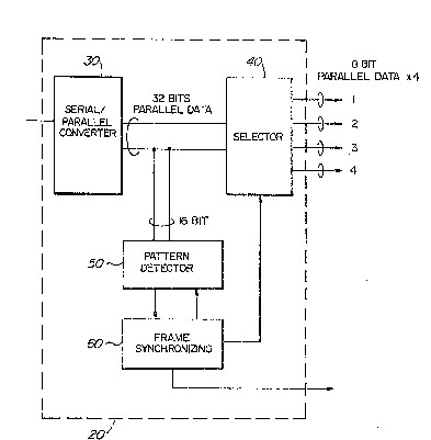
Figs. 5 and 6 are a general block diagram and a more
detailed block diagram, respectively, of an embodiment of the
present invention illustrating a frame pattern detection and
-- 5 --
frame synchronizing circult which utilizes the data pattern
illustrated in Fig. 4. In Figs. 5 and 6, serial/parallel
(S/P) converter 30 can comprise, for example, a shift
register. The serial/parallel converter 30 converts the byte
multiplexed frame bytes (serial data) to 32 bit parallel frame
bytes. In the embodiment shown in Fig. 5, the serial/parallel
converter 30 functions as a converting means. Pattern
detector 50 can comprise, for example, a comparator 52 and a
frame synchronization pattern register 54 (Fig. 6). In the
embodiment shown in Fig. 6, the comparator 52 and frame
synchronization pattern register 54 function as a pattern
detecting means. Referring to Fig. 6, comparator 52 compares
16 bit (two byte) groups output ~rom serial/parallel converter
30 with data representing the predetermined frame pattern
stored in frame synchronization pattern register 54. When
pattern detector 50 detects the two bytes of Fl and F2 forming
the predetermined frame pattern (indicated by A in Fig. 4)
from the parallel data output from serial/parallel converter
30, it outputs a DETECTION signal (e.g., a logic "1").
Frame synchronizing circuit 60 includes a counter 61
which begins counting upon receipt of the DETECTION signal,
and continues counting until it reaches a count equal to the
number of bytes in one frame (in the Fig. 4 data pattern, the
count equals 4). This number of COUIltS is called one frame
counting sequence (FCS). The counter 61 then stops counting
until another DETECTION signal is received. When the pattern
is detected again, the counter 61 begins counting again,
stopping after counting one FCS.
After each FCS, decoder 62 outputs an FCS signal, which
is input to a shift register 65. The FCS signal indicates
-- 6
2al
that an FCS has been completed. With each FCS signal, one of
the outputs of shift register 65 switches from a first logic
state to a second logic state (e.g., ~rom logic "O" to logic
"1"). After a predetermined FCS threshold number is reached
(for example, 7) all of the outputs of shift register 65 are
logic 1, causing an AND gate 66 to output a logic "1" to a
flip-flop 69. This sets flip-flop 69, causing it to output a
SYNC signal. Counter 61 receives the SYNC signal via OR gate
64, causing counter 61 to continue to count, even when
DETECTION signals are not received. This is known as backward
protection or backward 2rror analysis.
Once synchronized, the demultiplexer 20 continues to
monitor the input multiplexed data using forward protection or
forward error analysis, described hereinafter. If the frame
pattern is not detected for a predetermined threshold number
of times (called a "No Detection" or ND threshold number), the
outputs of the shift register 65 all switch to the first logic
state, for example, a logic "O". These outputs are invertPd
via inverters 68 and input to AND gate 67. AND gate 67
outputs, for example, a logic "1", reseting flip-flop 69, and
causing the counter 61 to revert back to counting only upon
receipt of a DETECTION signal. This continues until the FCS
threshold number is once again met. Thus, the forward and
backward error analysis assures that the pattern detection is
accurate before synchronizing, and also causes the
demultiplexer 20 to attempt to resynchronize upon loss of
synchronization.
As noted above, a selection signal SEL is generated
simultaneously with the detection of the predetermined frame
pattern. The selection signal SEL indicates the detection of
~98~
the frame byte corresponding to the last channel C4 of the
preceding frame. A decoder 63 detects the clock timing
indication, from clock 25, of the last byte of an FCS ( in this
example, the fourth byte). This byte corresponds to the
channel C4. Decoder 63 outputs a SEL signal to selector 40,
which can comprise, for example, a latch circuit. The
selector 40 functions as a selector means. Decoder 63, via
the SEL signal, causes selector 40 to associate the
multiplexed data with the proper channel and output it
accordingly.
In the Fig. 6 embodiment, shift register 65, AND gates 66
and 67, inverters 68 and flip-flop 69 function as a means for
outputting a signal indicating that a predetermined number of
FCS signals have been output by decoder ~2 and for outputting
the SYNC signal. This output means combined with counter 61,
OR gates 64, and decoders 62 and 63 function as a frame
synchronization means. When the predetermined number of
stages of protection are ac~uired (i.e., when the FCS
threshold is met), the SYNC signal is sent to a
synchronization terminal (not shown) indicating that
synchronization exists. Moreover, the SEL signal indicating
the last channel, for example, C4 is generated. Selector 40
outputs the data of channels C1 - C4 to their designated
output lines as 8 bit parallel sîgnals by selecting such data
in accordance with the SEL signal from the signal developed in
parallel in the serial/parallel converter 30.
As explained above, the predetermined frame pattern
comprising the last frame byte of one frame and the first
frame byte of a succeeding frame is detected as in the example
of Fig. 4. This simplifies the circuit for pattern detection.
1~8~20
Moreover, since the position of channel C~ can be recoynized
by this predetermined frame pattern detection, it is not
necessary to use a separate identification byte IC to identify
the channel numbers as in the prior art shown in Fig. 3A.
The system of the present invention is not limited only
to the case where the frame pattern is composed of two bytes
and may be formed by three or more bytes. In this case, the
frame synchronizing may be set by respective pattern detection
at the two or more boundaries.
The many features and advantages of the invention are
apparent from the detailed specification and thus it is
intended by the appended claims to cover all such features and
advantages of the invention which fall within the true spirit
and scope thereof. Further, since numerous modifications and
changes will readily occur to those skilled in the art, it is
not desired to limit the invention to the exact construction
and operation illustrated and described, and accordingly, all
suitable modifications and equivalents may be resorted to,
1~ falling within the scope of the invention.
. - - ' :' '' . ' ' ' , '
,
. .