Note: Descriptions are shown in the official language in which they were submitted.
`' ~ i~86;26
DIGITAL PHASE-LOCRl~D D:EVIC~: AND METHOD
DESCRIPTION
This invention relates to a digital phase-locked device and
method for synchronizing incoming data with a local clock, and
more particularly to a device and method wherein the stream of
data is phase locked to a local clock within a preselected number
of bit transitions in the data stream and wherein during
operation at different data rates, no calibration of the length
of a delay element string is required to insure that the total
0 delay time is equal to the local clock period.
Background of the Invention
U. S. Patent No. 4,677,648 to Zurfluh, assigned to the
~ assignee of the present invention, discloses a digital
: phase-locked loop wherein a chain of delay elements implements
: 1~ phase offset detection and clock signal phase shifting. No
sampling or control signals are used having a frequency higher
than that of the local master clock. However, continual
estimation is required of the number of delay elements in a delay
element string that is required for a delay time equal to one
period of the local clock; and a look-up table is required to
correct the phase offset to a phase selection value.
~. 1
In another case~ a digital phase-locked correction
loop is reset by subtracting one local clock cycle
whenever the buildup of successive delay increments
added to the system clock equals a full local clock
cycle.
SA9-88-018 Page 1
626
While these digital phase-locked devices operate
satisfactorily, there is a need for a device and method which
does not require any of the components required by analog or
digital phase-locked loops (e.g. VCOs, frequency multipliers,
phase detectors, microprocessors, comparators, etc.~ There is a
need for an improved device wherein phase locking of the incoming
data stream to the local clock can be achieved within a
preselected number of bit transi~ions, preferably an integral
multiple of a selection cycle corresponding to the number of
0 clock signals required to sequentially clock a register and a
selection register. There is also a need for a device and method
capable of operating at multiple data rates without requiring
that the length of a delay element string be calibrated or
recalibrated in order to insure that the total delay time will be
equal to the local clock period. Finally, it is desirable that
the phase-locked device be so compact and configured that it can
be implemented on a VLSI chip, while at the same time retaining
the feature of the above-cited prior art whereby no circuit
element operates at a frequency higher than that of the local
clock.
Summary of the Invention
Toward this end and according to the invention, the~e is
provided an improved digital phase-locked device and method for
synchronizing incoming data with a local clock. The device
includes a register which, when triggered during each successive
selection cycle, traps the states of waveforms supplied by a
delay element string. A transition detector detects transitions
in these waveforms and provides to a selection means a plurality
of outputs, each corresponding directly to a respective clock
position. The selection means provides a window defining the
SA9-88-018 Page 2
86Z6
maximum numher of unique clock positions adjacent a then present
clock position within which bit patterns are examined for
determining whether any of the clock positions then within the
window constitutes a valid local clock selection choice.
While operating in a locked condition, if a bit pattern
within said window is indicative of only one local clock
selection choice, that clock position is selected and locked as
the local clock. If the bit pattern in the window is indicative
of none or more than one local clock selection choice, then
0 unlocking of the phase lock will be deferred until at least the
next selection cycle. At any time during the deferral period, if
and when the bit pattern within window SW is indicative of only
one clock selection choice, that clock position will be selected
and locked as the local clock; otherwise unlocking will occur at
the end of the deferral period and relocking of the phase lock
initiated.
'~
During start up and during a wrap mode, a control means
clears a selection register forming part of the selection means
and enables a priority filter. This filter filters out from said
outputs of the transition detector all but one active bit and
unconditionally accepts the clock position corresponding to this
, single active bit as the then present clock position. ~Iowever,
operation during start-up and in the wrap mode differs in the
following respect.
During start-up, successive single active bit outputs of the
priority filter will be accepted unconditionally in sequence as
the then present clock position but no locking will occur until
the current output from the priority filter falls within the
selection window defined by the previous output; whereupon that
clock position corresponding to the current output will be
SA9-88-018 Page 3
`-` lZ~8~;~6
selected and locked as the local clock, and operation will
continue as above described Eor the locked condition.
In the wrap mode, however, the single active bit output of
the priority filter is used only once; i.e., the clock posltion
5 corresponding to the first single active bit output is
unconditionally accepted and locked as the local clock; whereupon
operation will continue as described for the locked condition.
Brie~ Description of the Drawings
'
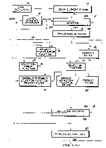
Fig. 1 is a schematic block diagram of a digital phase-lock
0 device embodying the invention.
Figs. 2A and 2B depict a clock sequence generator forming
part of the device of Fig. 1 and waveforms generated thereby,
respectively.
'~:
Fig. 3 depicts the logic diagram for a one-to-zero
transition detector forming another part of the device of Fig. 1.
Fig. 4 depicts the logic diagram for a priority filter
forming another part of the device of Fig. 1.
r~
Figs. 5A, 5B, 5C diagrammatically illustrate different
situations which occur when various bit patterns lie within a
selection window.
Description of Preferred EmhodLment
The digital phase-lock device embodying the invention
requires only an incoming data signal and a signal from a local
SA9-88-018 Page 4
,....
~Z9~36Z6
oscillator (such as a piezo-electric crystal) to synchronize the
data with a local clock. As lllustrated in Fig. 1, this device
comprises, briefly, a clock sequence generator 10 which generates
clock signals Co-C4 from an incoming data signal 8. Signals from
a local oscillator 9 are fed into a delay element string 11 to
generate a family of delayed clocks, each of which serves as an
input to a register means 12, comprising two registers or stages
12a, 12b. Register means 12, when triggered, traps the state of
the waveforms supplied by delay element string 11. A transition
detector 13 detects transitions in these waveforms and provides
to a selection means 14 a plurality of outputs.
Selection means 14 comprises, briefly, a priority filter 15,
priority filter error function logic circuitry 16, selection
function logic circuitry 17, selection error function logic
circuitry 18, a selection register means 19 having two registers
l9a, l9b, final selection logic circuitry 20, and control
circuitry 21 to condition a switch 22 to selectively connect
priority filter 15 or selection function circuitry 17 to
selection register 19.
The various components will now more specifically be
described. As illustrated in Figs. 2A and 2B, clock sequence
generator 10 generates five unique clock signals Co-C4 during
; each "selection cycle'i, which is defined as the predetermined
time period required to select a new local lock. The signals
Co-C4 are synchronized such that register 12a latches
responsively to signal C0, then register 12b latches responsively
to signal C1 and then again responsively to signal C2; whereupon
selection registers 19a, l9b are latched sequentially by signals
C3 and C~, respectively, to complete the selection cycle. Thus,
the registers 12a, 12b are latched alternately except that
SA9-88-018 Page 5
29~il6~6
register 12b latches twice successively; this is done in order to
eliminate an~ metastable outputs.
Mathematically, the above stated operating conditions placed
on the clock signals Co-C4 are stated by the following equation:
(Ci)(Cj) = O i ~ j, i=0,1,... 4, j=0,1,... 4, for all t>O, where t
is time.
The clock se~uence generator 10 comprises the digital
circuitry shown in Fig. 2A to generate these clock signals. It
consists of a five-bit shift register lOa which is clocked by the
0 incoming data in line 8. Each shift register bit, SO, S1, S2,
S3, and S4 corresponds to one of the five clock signals Co-C4~
which can only be active when the shift register bit is active
(i.e., "1"). Since the same conditions apply to SO, S1, S2, S3,
and S4 as apply to the clock signals,
(Si)(Sj) = O i ~ j, i=0,1,... 4, j=0,1,... 4, for all t>O.
The logic circuitry in clock sequence generator 10 insures
that the shift register lOa is always set so that the above
conditions are met. The single successive bits of shift register
_ _ _f _ _
lOa are then continuously cycled to produce, from the five inputs
So-S4, four clock signals Co-C4. Only four clock signals are
generated because at lOb the shift register bits S1 and S2 are
~; OR'd before the shift register bits, SO, (S1 or S2), S3 and S4
are ANDed at lOc-lOF with the incoming data. The CO, (Cl or C2),
outputs condition the registers 12a or 12b as above explained.
~5 The outputs C3 and C4 are fed via line 23 to condition the
selection registers l9a, l9b.
SA9-88-018 Page 6
IL2986;2~i
The total delay time through delay element string 11 must be
at least equal to one period of the local oscillator 9. So, if N
is the number of selectable clock positions and N-1 constitutes
one period of oscillator 9, then two extra delay elements N and
N+1 are added in string 11 to insure that at least a single
one-to-zero (or zero-to-one) transition can be detected by the
transition detector 13, for reasons that will become apparent.
Delay element string 11 generates, in well known fashion from a
plurality of series-connected delay elements, a family of delayed
0 waveforms. Each consecutive waveform is separated by the
preselected delay time td between adjacent delay elements. At
the end of a selection cycle, one of these delayed clocks (0-N)
will be chosen as the local clock 24.
The number of bits in each register 12a, 12b is equal to
N+1, the number of wa~eforms supplied by delay element string 11.
When register 12a is triggered by the clock signal C0, it traps
the states of the waveforms supplied by the delay string 11.
Since signal CO is generated by a data transition, the state of
register 12a can be evaluated to determine the phase offset. The
data in register 12a becomes available when register 12b is
clocked by signal C1. As earlier noted, register 12b is clocked
a second time by signal C2 to eliminate any metastable outputs.
. ~ , _
Transition detector 13 (see Fig. 3) comprises combinational
logic designed to detect one-to-zero transitions in registers
12a, 12b. These transitions indicate those delay clock signals
which are aligned with the data. Transitions are detected from
the low order (leftmost) bit to the high order (rightmost) bit.
In the transition detector 13, the last bit position N+1 is lost.
The highest order bit, N+1, cannot contain a transition, since
there is nothing to compare it with. Thus, the output of the
SA9-88-018 Page 7
986Z6
transition detector 13 has N bits Ibit positions 0-N), one less
bit than the N-~1 bits in registers 12a, 12b, and the total delay
is at least one full period of oscillator I plus one extra bit
position -- the reason two extra delay elements were added as
above stated. As illustrated in Fig. 3, the left bit inputs to
each AND gate are non-inverted and the right bit inputs are
inverted. However, if preferred, these right and left bit inputs
may be reversed if it is desired that the transition detector 13
detect one-to-zero transitions. Each output from transition
detector 13 corresponds directly to a respective clock position.
The various components of selection means 14 and their
interaction will now be described. Priority filter 15 (see Fig.
4) filters out from the outputs of transition detector 13 every
bit valued at "1" except the first bit detected in the output.
J 5 ( As illustrated, this is the lowest order bit, however, if
preferred, it could be the hightest order bit.) Thus the output
of filter 15 contains only a single active (i.e., "1") bit,
corresponding to a single delayed clock signal from the delay
element string 11. Switch 22 is conditioned by control means 21
to enable priority filter 15 only when the phase-lock device is
starting up, in a wrap mode, or relocking; otherwise, switch 22
; is conditioned by control means 21 to enable the selection
function. While both the priority filter i5 and~selection logic
17, 18 operate continuously, only one at a time is selectively
enabled. Operation under these various conditions will hereafter
be described.
Selection function logic 17 has a number of outputs equal to
the number of inputs supplied by transition detector 13; and each
such output corresponds directly to a clock position. For
example, output 5 of selection logic 17 corresponds to clock
SA9-88-018 Page 8
9~62~
position 5. During each selection c~cle, selection function
logic 17 supplies the next clock selection based on the present
clock selection and the inputs supplied by transition detector
13. Since only one selection output from the selection logic 17
may be active (i.e., a"1") at any one time, there can be only one
clock position selected at any such time.
The selection function logic 17 is based on a "selection
distance" SD which is preselected and defined as the maximum
number of unique clock positions to either side of the present
0 position which constitute a valid clock selection. For example,
as illustrated in Fig. 5A, if the present clock selection is
clock 5 (see bit 5~, and the selection distance is 1, then clock
numbers 4, 5, 6 (corresponding to bits 4, 5, 6) would be valid
choices. As illustrated, then, the selection distance SD defines
15 a "symmetric selection window" SW which has length three clock
positions. While desirable it is not essential however, that the
selection distances to the right and left of the present clock
position be equal.
The bit patterns within selection window SW and the current
20 clock selection are used to derive the equations for the
selection function logic 17 and thus determine a clock selection.
The number of bit patterns found within selection window~SW must
be less than 2(Sw), since transition detector 13 prevents the
appearance of two consecutive active (i.e., "1") bits. Where
2~ SW=3 (as illustrated) or more, this number of bit patterns will
be less than 2(Sw) by e~clusion of all patterns where there are
two or more adjacent "1" bits.
SA9-88~018 Page 9
36Z6
The selection equa~ions are of two distinct types:
conforming and nonconforming. The "conforming equations" have
the same form, because identical bit patterns are used by these
equations to select a clock. The "nonconforming equations" are
5 confined to the 0,...,SD and N-SD,...N positions, where SD is the
selection distance and N is the highest order (or last)
selectable clock position. As illustrated, then with SD=1, the
nonconforming e~uations would apply to the 0 and 1 clock
positions and the N-1 and N clock positions. These nonconforming
0 equations occur because the bit patterns within selection window
SW have special characteristics due to their endmost positions,
where the bit patterns are unique and thus require equations that
are unique.
.
The conforming equations and nonconforming equations are
discussed in Appendix A.
Figs. 5A, 5B and 5C depict three different situations that
- can occur when bit patterns within selection window SW are being
examined. In each case, assume that the device is phase locked
and that the present clock position as identified in selection
20 register 19 is in the center of window SW (bit position 5). Note
that only one selection register bit position can be active at a
time. This guarantees that only one clock can be selected as the
data clock.
~ .
Assume now that the output from transition detector 13 to
~5 selection register 19 is a "1" in bit position 6 and that there
are "O's" in bit positions 4 and 5, as shown in Fig. 5A. Since
there is only one valid choice (the single "1" bit) in window SW,
the window will move rightward to bit position 6 in which the
"l's" are aligned; clock position 6 will be selected and locked
SA9-88-018 Page 10
986Z6
as the valid selection choice for local clock 24, and no error
will be generated. If the sample "1" in the transition detector
output had been in bit position 4, window SW will move leftward
to align the "l's"; and if in bit position 5, window SW will
remain stationary. During each successive selection cycle, bit
pattern reexamination will be repeated.
Assume now that instead o only one "1" in window SW, the
output from transition detector 13 includes "l's" in two window
bit positions (e.g., 4 and 6, as illustrated in Fig. 5B) or that
0 all bits in the window are "O's". In such event, window SW will
not move, and a correctable error signal will be generated by
selection error function logic circuitry 18. A correctable error
is defined as one in which more than one clock selection choice
(i.e., more than one "1" or no "l's") lie within selection window
- 15 sw.
In the situations described in connection with Figs. 5B and
5C (i.e~, where there is more than one "1" or there is no "1"
within window SW), the device will remain locked and window SW
will not move until at least the next selection cycle; whereupon
the bit pattern will be reexamined to see if there is now a
single "1" bit in window SW indicative of a valid clock selection
choice. The number of successive selection cycles during which
an unlocking decision is deferred for successive errors (whether
correctable, conditional or a combination of both) is preselected
SA9-88-018 Paye 11
1~86Z~;
by the circuit designer, and may differ for the various types of
errors as programmed or hardwired in the control logic circuitry
21.
Circuitry 21 preferably is provided by a so-called Moore
5 finite state machine. This finite state circuitry 21 is clocked
by sequence generator 10 and responsive to inputs from the
selection error logic circuitry 18 and priority filter error
logic circuitry 16, during the then present or current state, to
condition switch 22 to selectively enable either the selection
logic or the priority filter.
As earlier noted, selection register 19 receives data from
either the priority filter 15 or the selection function logic
circuitry 17. When register l9a is triggered by the clock signal
C3, the input data is trapped. This data, which corresponds to a
15 clock selection choice, becomes available to selection register
19 when register 19b is triggered via line 23 by clock signal C4.
Then the 0,.... ,N bits of selection register 19 are ANDed with the
~`~ respective 0,.. ..,N delayed clock signals from delay element
string 11. However, only one of the clock signals produced by
20 string 11 is enabled because only one of the 0,...,N selection
bits will be active (i.e., a "1"). All 0,...,N outputs resulting
from the ANDing are OR'd together to produce a single local clock
output signal in line 24.
~; In operation, during start up, control circuitry 21
25 conditions switch 22 to clear selection register 19 forming part
of selection means 17, 18, 19 and enables priority filter 15.
Filter 15 filters out from the outputs of transition detector 13
all but one active bit and unconditionally accepts the clock
position corresponding to this single active bit as the then
SA9-88-018 Page 12
-" ~L29E~26
present clock position. Successive single active bit outputs o~
priority filter 15 will be accepted unconditionally in sequence
as the then present clock position but no locking will occur
until the current output from the priority filter falls within
the selection window SW defined by the previous output; whereupon
that clock position corresponding to the current output will be
selected and locked as the local clock. In other words, the
device will remain in start-up mode until locking is eventually
achieved.
0 While operating in a locked mode, if a bit pattern within
selection window SW is indicative of only one local clock
selection choice, that clock position is selected and locked as
the local clock. If the bit pattern in window SW is indicative
of none or more than one local clock selection choice, then
unlocking of the phase lock will be deferred until at least the
next selection cycle. The number of selection cycles unlocking
is deferred if no valid clock selection choice is indicated is
preselected by the designer. At any time during the deferral
period, if and when the bit pattern is indicative of only one
20 clock selection choice, that clock position will be selected and
locked as the local clock; otherwise unlocking will occur at the
end of the deferral period and relocking of the phase lock
initiated. Relocking is achieved by repeating t~e start-up
procedure.
The single active bit in the selection register
corresponding to the then current clock position is always
centered in selection window SW, as shown in Figs. 5A, B, C. If
the selection window SW is moved incrementally leftward to where
this single active bit is at bit position 0 (or rightward to bit
~0 position N), the wrap mode will be initiated. When in wrap mode,
SA9-88-018 Page 13
~29E~6;~6
selection register 19 will be cleared and priority filter 15
enabled as during start-up. However, the single active bit
output of priority filter 15 is used only once; i.e., the clock
position corresponding to the first single active bit output is
unconditionally accepted and locked as the local clock; whereupon
operation will continue as described for the locked mode.
In the embodiment illustrated, each selection cycle
consisted of five data periods. However, if preferred, this
number may be increased to any desired odd number, the odd number
0 being required to permit register 12b to latch twice successively
to eliminate any metastable outputs. Also, while the data -
depicted in Fig. 2B has a uniform data rate, it is to be noted
that the digital phase-locked device herein disclosed does not
require a uniform data rate; it can be used with encoded data
such as that produced by a run length limited transmission code.
For use with multiple data rates, the total delay time through
the delay element string 11 must, of course, be at least equal to
the bit period of the slowest expected data rate.
:;
It will be understood that the foregoing and other changes
may be made in the digital phase-locked device and method herein
describ~d. The embodiment illustrated is therefore to be
considered merely illustrative and the invention is not to be
considered limited except as specified in the claims.
SA9-88-018 Page 14
129~;26
APPENDIX A
I. SELECTION LOGIC DURING LOCKED OPERATIONS
Conforming Equation
Assume as in: FIG. SA FIG. 5B FIG. 5C
5 SELECT REG. Ax-1 ~x x+l AX_2 AX_l Ax x x+1 A~+2
CURRENT CHOICE 0 1 0 0 1 0 0 1 0
TRANSITj DET- Bx_1 Bx x+1 Bx-2 Bx-1 x Bx Bx-1 Bx+2
o 1 o o o 1 1 o o
SAMPLE 0 0 0
0
TO SR Ax-1 Ax Ax+1 Ax-2 Ax+1 Ax x x+1 Ax+2
NEXT CHOICE0 1 0 0 0 1 1 0 0
If x is the eurrent bit position ehoice in the selection
register, and is any integer between and including 2 and N-2, the
selection logic equation for bit position x will be:
SEL~=AX(BX~ BX+l) + Bx(AX+l Bx+2 + Ax-1 Bx-2)
The transition detector 13 output eannot have two or more
: 20 eonsecutive l's; thus the following patterns 0 1 1, 1 1 0 and
1 1 1 will not be found in window SW.
Although, 0 0 0 and 1 0 1 are legitimate patterns which may
occur within the window, they imply that the nex~ choice-~is
outside the window (0 0 0) or that there is metastability (1 0
1). Thus, they are recorded as errors and the eurrent seleetion
remains. Decision to unlock will be deferred at least one more
selection cycle to provide opportunity to reeover.
:
~ SA9-88-018 Page 15
lZ98~i2~
Nonconforming Equations
Assume as below; then current Assume as below; then
choice will be held at A . window will move left and
1 give next selection cycle
one more chance to
correct.
SR Ao A1 A2
CURRENT CHOICE 0 1 0
TD 0 1 B2
10SAMPLE 1 0 0
TO SR A1 A2
NEXT CHOICE 1 0 0
SELo = A1 Bo B2
~ .
:
SR Ao A1 A2 A1 A2 A3
0 1 0 0 1 0
:`~
~ TD B1 B2 B1 B2 B3
:~i O 1 0 1 0 0
o o o
o
o
CAN'T OCCUR 1 1 0
SR 1 A2 1 A2 A3
0 1 0 1 ~ O
SEL1=Al(Bo ~+'B2) + A2B1 3
SA9-88-018 Page 16
Z~3~626
Assume as below; then current Assume as below; then
choice will be held at ~-1 window will move right
and give next selection
cycle one more chance to
correct.
SR AN_2 ~N-l AN
CURRENT CHOICE 0 1 0
TD BN_2 ~3N-l BN
SAMPLE 0 0
i0 TO SR AN_2 AN_l AN
NEXT CHOICE 0 0
SELN = AN_l BN BN-2
SR AN_2 AN_l AN AN_3 AN_2 AN_
. 1~ o 1 o o 1 o
TD BN_2 BN_l BN BN_3 BN_2 BN_
0 1 0 0 0
O O O
1 o
o
CAN'T OCCUR 1 1 0
SR AN_2 AN_l AN Al ~ A2 A~
0 1 0 0 0
N-l AN-1(BN(~ 3N-2) + ~-2BN-lBN-3
.
~ SA9-88-018 Page 17
~-`` 12~8~Z~
II. SELECTION ERROR FUNCTION
Conforming E~uation
If x is the current bit position selection choice and is any
integer between and including 1 and N, the selection error
: 5 function equation for position x will be:
SEFx AX[(Bx_l ~ BX_l) (BX_l + Bx)]
There is no nonconforming equation for Selection Error
Function (SEF). Ao cannot be in the center of window SW. If Ao
is the current choice, then wrap mode is initiated.
SA9-88-018 Page 18
~Z986Z6
III. PRIORITY FILTER ERROR FUNCTION
Conforming Equation
Again, assuming that x is between and including 1 and N-l
and denotes the bit position corresponding to the current
selection, and that A denotes the selection register and B
denotes the transition detector, then the priority filter error
function equation is:
_
PFEF=AxBx-lBxBx~l
The priority filter output can have only a single active
bit. Thus, the patterns 1 0 1, 1 1 1, 0 1 1, 1 1 0, will not be
found within the window.
; This means that the only detectible error condition will
occur if
x-l Bx Bx+l
o o o
PFEF will equal 1, denoting error
Nonconforming Equation
This relates to the following condition
: Ao Al AN_l AN
1 o o
0 Bl N-l BN
0 0 PFEF=l 0 0
Then PFEF-AoBoBl~ and PFEF= ~ BN lBN
SA9-88-018 Page 19
" ~Z91516Z~
Note that the priority filter output can have only a single
active bit. Thus, the pattern 11 will not be found within the
window. Window SW may remain in the same position or move
rightward from Ao or leftward from AN. If x is the current bit
position choice in the selection register, and is any integer
between and including 1 and N-l, the priority filter error
function equation will be:
PFEF AxBx-lBxBx~l + ABBl ~ BN-lBN
SA9-88-018 Page 20