Note: Descriptions are shown in the official language in which they were submitted.
~.Z~38639
PIN JUNCTION PHOTOVOLTAIC ELEMENT WITH P OR N-TYPE
SEMICONDUCTOR LAYER COMPRISING NON-SINGLE CRYSTAL
MATERIAL CONTAINING Zn, Se, Te, H IN AN AMOUNT OF'
1 TO 4 ATOMIC ~ AND A DOPANT AND I-TYPE SEMI-
CONDUCTOR LAYER COMPRISING NON-SINGLE CRYSTAL
SI(H,F) MATERIAL
FIELD OF THE INVENTION
The present invention relates to an improved photo-
voltaic element which is usable as a power source for
electric appliances and also as a power generator. More
particularly, it relates to an improved pin junction photo-
voltaic element with a p-type or n-type semiconductor layer
comprising a non-single crystal material containing zinc
atoms, selenium atoms, tellurium atoms, hydrogen atoms ln
an amount of 1 to 4 atomic % and a dopant and an i-type
semiconductor layer comprising a non-single crystal SitH,F)
material which exhibits a high photoelectric conversion
efliciency particularly for short-wavelength light.
'
~ - 1- ~
~Z913~;39
~ACKGROUND OF THE INVENTION
There have been proposed a variety of pin junction
photovoltaic elements for solar cells and for power sources
in various electric appliances. Such photovoltaic elements
are formed by ion implantation or thermal diffusion of an
impurity into a single crystal substrate of silicon (Si) or
gallium arsenide (GaAsj, or by epitaxial growth of an
impurity-doped layer on said single crystal substrate.
However, there is a disadvantage for these photovoltaic
elements that their production cost unavoidably becomes
costly because of using said specific single crystal
substrate. Because of this, they have not yet gained
general acceptance for use as solar cells or as power
sources in electric appliances.
Recently, tl~ere has been proposed a photovoltaic ele-
ment in which there is utilized pin junction of amorphous
silicon (hereinafter referred to as "A-Si") deposited film
formed on an inexpensive non-single crystal substrate of
glass, metal, ceramic or synthetic resin by way of glow
discharge decomposition method. This photovoltaic element
has a nearly satisfactory performance and is of low produc-
tion cost and because of this, it has been recognized
usable as a power source for some kinds of appliances such
as electronic calculators and wrist watches.
However, for this photovoltaic element, there is a
disadvantage that the output voltage is low because the
-- 2
~29~3639
band gap of the A-Si film constituting -the element is about
1.7 eV, which is no-t large enough. There is another dis-
advantage that its photoelectric conversion efficiency is
low for a light source such as fluorescent light which
contains short wavelength light in a dominant proportion,
so that its application is limited to appliances with very
small power consumption.
There is a further disadvantage for said photovoltaic
element that the constituent A-Si film is often accompanied
with a character of the so-called Staebler-Wronsk effect,
with which the film being deteriorated upon continuous
irradiation with intese light for a long period of time.
~ or a photovoltaic element to be immobilized as a
power solar cell, it is necessary to convert efficiently
and continuously the light energy of sunlight into the
electric energy, and hence, it is desired to have such a
layer structure that permits photoelectric conversion for
sunlight over as broad a spectrum range as possible.
Now, in the case of a photovoltaic element which is
made using a semiconductor material having a small energy
band gap, the wavelength region of light to be absorbed by
-the layer is extended from the short wavelength side to the
long wavelength side. However, in this case, it is the
long-wavelength component of sunlight alone that
contributes to photoelectric conversion, and the energy of
363~1
the short-wavelength component is not served for
photoelectric conversion. This is because the amount of
energy to be outputted by the photoelectric conversion is
decided upon the energy band gap of the semiconductor
material as used.
On the other hand, in the case of a photovoltaic
element which is made using a semiconductor material having
a large energy band gap, the wavelength component which is
absorbed by the layer and comes to contribute to
photoelectric conversion is the short wavelength light
having an energy exceeding the energy band gap of the
semiconductor material as used, and the long-wavelength
component is not served for photoelectric conversion.
By the way, in a photovoltaic element, the maximum
voltage or open-circuit voltage (Voc) to be outputted is
determined upon the energy band gap values of the semi-
conductor materials to be joined together. In view of
this, in order to obtain a high Voc, semiconductor
materials having a great energy band gap are desired to be
used.
Therefore, there is eventually a limit for the photo-
electric conversion efficiency for a photovoltaic element,
which is prepared by using the sole semiconductor material.
The foregoing led to an idea of forming a plurality of
photovoltaic elements using a plurality of semiconductor
4 -
materials each having a different energy band gap, so that
the individual photovoltaic elements become responsible for
the different wavelength regions of sunlight. This idea
was expected to contribute to an improvement in the photo-
electric conversion efficiency.
However, there is a disadvantage for the solar cell
having such layer structure as mentioned above that the
high photoelectric conversion as a whole is possible on~y
in the case where the individual photovoltaic elements have
good characteristics, because it is of such structure that
a plurality of photovoltaic elements are stacked to forrn an
electrically serial structure.
Unfortunately, for the photovoltaic element having the
~oregoing structure, there has not yet realized any
desirable one that the respective constitutent elements as
stacked have satisfactory values of energy band gap and
satisfactory characteristics as desired and that provides a
high Voc as the photovoltaic element.
Besides, there have been proposed direct transition-
type semiconductor films having a wide band gap, such as
ZnSe (having a band gap of 2.67 eV) and ZnTe (having a band
gap of 2.26 eV) and mixed crystal thereof ZnSe1 xTex (where
O<x<l). And the public attention has been forcused on
these semiconductor films. These semiconductor films are,
in general, such that are formed on a single crystal sub-
strate by way of epitaxial growth. The as-grown film of
ZnSe exhibits n-type conductivity and the as-grown film of
ZnTe exhibits p-type conductivity. However for any of
these films, it is generally recognized that it is
difficult for the film to be controlled to the opposite
conductivity. Further, in order to carry out the epitaxial
growth upon the film formation, it is required to use a
specific single crystal substrate and to maintain the
substrate at elevated temperature. And in this film
formation, the deposition rate is low. Because of this, it
is impossible to perform epitaxial growth on a commercially
available substrate which is inexpensive and low heat-
resistant such as glass and synthetic resin. These factors
make it difficult to develop practically applicable
semiconductor films using the foregoing commerically
available substrates.
Even in the case where a semiconductor film should be
fortunately formed on such commercially available
substrate, the film will be such that is usable only in
very limited applications.
There have been various proposals to form a direct
transition-type semiconduc-tor film on a non-single crystal
substrate such as glass, metal, ceramics and synthetic
resin. However, under any of such proposals, it is
difficult to obtain a desired direct transition-type
:
- 6 -
1~9~3~3~
semiconductor film having satisfactory electrical
characteristics because the resulting film becomes to be
accompanied with defects of various kinds which make the
film poor in electrical characteristics and on account of
this, it is difficult for the film to be controlled by
doping it with an impurity.
In the meantime, amorphous film comprised of Zn and Se
elements can be found in prior art references. As such
prior art references, there are U.S. Patent No. 4,217,374
(hereinafter,called "literature 1") and U.S. Patent No.
4,226,898 (hereinafter, called "literature 2"). And ZnSe
compound is described in Japanese Patent Laid-open No.
189649/1986 (hereinafter, called "literature 3") and
Japanese Patent Laid-open No. 189650/1986 (hereinafter,
called "literature 4").
Now, literature 1 discloses amorphous semiconductor
films containing selenium (Se) or tellurium (Te), and zinc
(Zn), hydrogen (H) and lithium (Li); but the subject lies
in amorphous selenium semiconductor film or in amorphous
tellurium semiconductor film, and the Zn described therein
is merely an additive as well as Li and H. And as for the
Zn and the Li, likewise in the case of the H, they are used
aiming at reduction of the local state density in the
energy band gap without changing the inherent
characteristics of the film. In other words, the
~291~639
incorporation of Zn into the amorphous Se or the amorphous
Te in literature 1 is not intended to positively form a
ZnSe compound or a ZnTe compound. Incidentally, literature
1 mentions nothing about the formation of a ZnSe compound,
ZnTe compound, ZnSe1 xTex compound, ZnSe crystal grains,
ZnTe crystal grains or ZnSe1 xTex crystal grains. And as
for the addition of Li, it should be noted that it is not
added as a dopant.
; Literature 2 does mention amorphous semiconductor
films containing Se or Te, and Zn, and H. However, it
deals mainly with amorphous silicon, and it defines Se and
Te as elements to form a compound with said silicon. As
for the Zn, it defines as an element to sensitize the
photoconductivity and reduce the local state density in the
energy gap. In other words, the additions of Zn and Se are
not intended to form a ZnSe compound, ZnTe compound or
ZnSel xTex compound. Incidentally, li-terature 2 mentions
nothing about the formation of a ZnSe compound, ZnTe
compound, ZnSel xTex compound, ZnSe crystal grains, ZnTe
crystal grains or ZnSe1 xTex crystal grains.
Literature 3 and literature 4 are concerned with the
deposition of a ZnSe film by HR-CVD method (hydrogen
radical assisted CVD method). That is, they disclose
methods of improving the deposition rate and the
productivity of a deposited film; and they merely mention
-- 8
productivity of a deposited film; and they merely mention
deposited films of non-doped ZnSe.
Against these backgrounds, there is an increased
social demand to provide an inexpensive photovoltaic
element having a high photoelectric conversion efficiency,
particularly, for short-wavelength light which may be
practically usable as solar cell and also as a power source
in various electric appliances.
SUMMARY OF THE INVENTION
The present invention is aimed at solving the afore-
mentioned problems relating to photovoltaic elements for
use in solar cells and other appliances and satisfying the
foregoing social demands.
It is therefore an object of the present invention to
provide an improved pin junction photovoltaic element
usable in devices typified by solar cell with the use of an
improved functional deposited film which may be desirably
formed even on a commercially available inexpensive non-
single crystal substrate of glass, metal, ceramic or
synthetic resin and which may form a desired pin junction
with other films to be formed on such substrate.
Another object of the present invention is to provide
an improved pin junction photovoltaic element whlch
-
39
provides a high photoelectric conversion particularly for
short-wavelength light and which is usable in devices
typified by solar cell
; A further objec-t of the present invention is to
provide an improved pin junction photovoltaic element with
a p-type or n-type semiconductor layer comprising a non-
single crystal material containing zinc atoms, selenium
atoms, tellurium atoms, hydrogen atoms in an amount of 1 to
4 atomic ~ and a dopant of p-type or n-type and an i-type
semiconductor layer comprising a silicon-containing non-
single crystal film, which exhibits a high photoelectric
; conversion efficiency particularly for short-wavelength
light and which is effectively usable particularly as solar
cell.
~,~
BRIEF DESCRIPTION OF THE DRAWINGS
,FIG. 1( A) is a schematic cross-sectional view of a
typical pin junction photovoltaic element according to the
~;present invention.
FIG. l(B) is a schematic cross-sectional view of
another typical pin junction photovoltaic element according
to the present invention
~L2~
FIG. l(C) is a schematic cross-sectional view of a
typical multi-cells stacked photovoltaic element according
to the present invention.
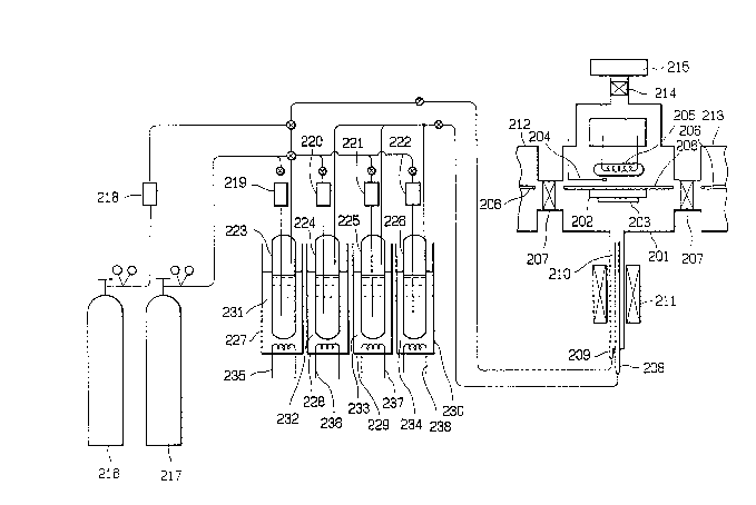
FIG. 2 is a schematic diagram to illustrate a
representative apparatus suitable for practicing the later
described process (1) of forming a constituent layer for
any of the above photovoltaic elements according to the
present invention.
FIG. 3 is a schematic diagram to illustrate a
representative apparatus suitable for practicing the later
described process (2) of forming a constituent layer for
any of the above photovoltaic elements according to the
present invention.
FIG. 4 is a schematic diagram to illustrate a re-
presentative apparatus suitable for practicing the later
described process (3) of forming a constituent layer for
any of the above photovoltaic elements according to the
present invention.
FIG. S is a graph showing the interrelation between
the content of hydrogen atoms (H) and the proportion of
crystal grain domains for a ZnSe1_xTex:H filrn in
Experiments A(2) and A(3).
FIG. 6 is a graph showing the interrelation between
i3~3
the content of hydrogen atoms (H) and the ratio o~ the
change in conductivity for a ZnSe1 xTex:H film in
Experiment B.
FIG. 7 is a graph showing the interrelation between
the content of hydrogen atoms (H) and the drift mobility of
holes for a ZnSe1 xTex:H film in Experiment B-
FIG. 8 is a graph showing the interrelation betweenthe content of hydrogen atoms (H) and the dark conductivity
for a ZnSe1_xTex:H:Li film in Experiment C.
FIG. 9 is a graph showing the interrelation between
the proportion of crystal grain domains and the content of
hydrogen atoms for a ZnSe1 xTex:H:Li film in Experiment C.
FIG. 10 is a graph showing experimental results with
respect to the reproducibility of a ZnSel xTex:H:Li film
having a desired property in Experiment C.
FIG. 11 is a graph showing the interrelation between
the content of hydrogen atoms (H) and the dark conductivity
for each of a various p-type doped ZnSel xTex:H films with
the quantitative ratio of Se to Te in the film being a
parameter in Experiment D.
FIG. 12 is a graph showing the interrelation between
the quantitative ratio of Se to Te and the dark
conductivity for a p-type doped ZnSe1 xTe:H film in
Experiment D.
FIG. 13 is a graph showing the interrelation between
- 12 -
:~2~
the quantitative ratio of Se to Te and the dark
conductivity for an n-type doped ZnSel xTex:H film in
Experiment E.
FIG. 14 is a graph showing the interrelation between
the quantitative ratio of Se to Te and the optical band gap
for a ZnSel xTex:H film in Experiment F.
FIG. 15 is a graph showing the interrelation between
the quantitative rartio of Se to Te and the proportion of
crystal grain domains for each of a non-doped ZnSel xTex:H
film, Ga-doped ZnSel xTex:H film and Li-doped ZnSel xTex:H
film.
DETAILED DESCRIPTION OF THE INVENTION
The present inventors have made extensive studies for
overcoming the foregoing problems not only on the known
ZnSe film but also on the known ZnSel xTex film for use in
various appliances such as solar cell and attaining the
objects as described above and as a result, have
accomplished the present invention based on the findings
obtained through various experiments as below described.
That is, as a result that there was prepared a
ZnSe1 xTex deposited film in which the quantitative ratio
of Se to Te being controlled to a specific value, a
- 13 -
~9~;39
specific amount of hydrogen atoms being incorporated and
the proportion of crystal grain domains per unit volume
being controlled to a specific value (this deposited film
is hereinafter referred to as "ZnSe1 xTex:H film"), the
present inventors have found the facts that (a) said
ZnSe1 xTex:H film is a non-single crystal film which may be
formed in a desired state even on a non-single crystal
substrate of glass, metal, ceramic or synthetic resin: (b)
the ZnSe1 Tex:H film formed on such non-single crystal
substrate is accompanied with very few defects: (c) it can
be easi.ly and efficiently doped with a dopant of p-type or
n-type: and (d) when doped with a p-type dopant, there is
afforded a desirable p-type ZnSe Te :H semiconductor film
l-x x
having a wealth of many practically applicable
semiconductor characteristics.
The present inventors have found further facts that in
the case of using the foregoing ZnSel xTex:H film as a
member for pin junction in the preparation of a pin junc-
tion photovoltaic element, there is affored a pin junction
photovoltaic element which efficiently and stably generates
a desired photoelectromotive force.
The present invention has been completed on the basis
of these findings, and it provides pin junction photo-
voltaic elements as below mentioned;
(1) a pin junction photovoltaic element which comprises a
- 14 -
3~
p-type semiconduc-tor layler, an i-type semiconductor layer
and an n-type semiconductor layer being stacked,
characterized in -that at least said p-type semiconductor
layer or said n-type semiconductor layer comprises a
deposited film comprised of zinc atoms, selenium atoms,
tellurium atoms and at least hydrogen atoms and which
contains a p-type or n-type dopant: the quantitative ratio
of said selenium atoms to said tellurium atoms in said
deposited film is in the range of from l:9 to 3:7 in terms
of atomic ratio: said deposited film contains said hydrogen
atoms in an amount of 1 to 4 atomic ~: and said deposited
film contains crystal grain domains in a proportion of 65
to 85 vol ~ per unit volume: and said i-type semiconductor
layer comprises (a) a non-single crystal film containing
silieon atoms as the matrix and at least one kind selected
from the group consisting of hydrogen atoms and fluorine
atoms or (b) a non-single erystal film eontaining silieon
atoms, at least one kind selected from the group eonsisting
of carbon atoms and germanium atoms, and at least one kind
selected from the group eonsisting of hydrogen atoms and
fluorine atoms;
(2) the pin junction photovoltaic element as defined in
the above (1), wherein said p-type dopant is a member
selected from the group consisting of Group I elements and
Group V elements of the Periodic Table; and
- 15 -
~;9~363~
(3) the pin junction photovoltaic element as defined in
the above (2), wherein said member is lithium.
The experiments carried out by the present inventors
to obtain the foregoing findings will be detailed in the
following.
Experiment A: Observations on the proportion of crystal
grain domains as formed in a ZnSel_xTex deposited film
when hydrogen atoms are introduced thereinto
(1) Preparation of samples
(i) There wexe provided two kinds of substrates; (a)
a p-type round silicon wafer of 0.5 mm in thickness and 1
inch in diameter (having an electrical resistivity (p) of
about 10 1 Q-cm), on which is formed an SiO2 film of about
5000 A in thickness, by way of the known thermal oxidation
treatment in an oxygen gas stream at 1000C and (b) a
square quartz glass of 2.5 cm by 2.5 cm in size.
(ii) The above-mentioned two substrates were placed
side by side on the substrate holder 202 of the known
apparatus as shown in Fig. 2. On every substrate was
formed a ZnSel xTex:H film under the conditions shown in
Table 1. Thus, there were obtained samples Nos. 1 - 12 ~on
substrates (a)] and samples Nos. 1' - 12' [on substrates
(b)]-
- 16 -
i39
(iii) Each of samples Nos. 1 - 12 (deposited on
silicon wafers) was cut in half. Each of the cut halves
was cut to a ~ mm square size which matches the holder of
the known transmission electron microscope (TEM). The cut
piece was fixed to a glass plate, measuring 50 mm by 50 mm
and 1 mm thick, by the aid of wax, with the deposited film
in contact with the glass surface so that the deposited
film is visible through the opposite side of the glass
plate.
(iv) The exposed part comprising silicon single
crystal wafer of the sample as prepared in (iii) was etched
with an a~ueous solution contining HF, HNO3, and CH3COOH.
The etching rate was properly controlled by chaning the
concentration of HF in the etching solution. Etching was
continued until the silicon single crystal wafer was
completely removed. In this case, the progress of the
etching was confirmed by observing the light passing
through the deposited film.
(v) Aftex e~ching, the wax was rernoved by the aid of
an organic solvent (toluene), and the deposited film was
separated from the glass plate, followed by rinsing and air
drying. Thus there was obtained a film specimen composed
of an SiO2 film and a ZnSel xTex:H film thereon.
(2) Examination of the film specimens prepared in (1)
~29~3639
Each film specimen of samples Nos. 1 - 12 formed on
silicon wafers in the above step (1) was examined by fixing
it to the sample holder of the TEM (acceleration voltage:
200 KeV) to form a transmission image and observing the
resultant -transmission image. As a result, it was found
for the resultant transmission image that there is a
lattice image with very few lattice defects in the part of
the ZnSe1_xTex:H film where crystal grain domains exist.
It was also found that the lattice images are uniformly
distributed throughout the ZnSel xTex:H film.
The lattice image was utilized to determine the
proportion of crystal grain domains in a certain area of
the film specimen. Thus the proportion in terms of volume
percentage (vol%) of the crystal grain domains present in
the deposited film was calculated.
For the purpose of reference, the direction of the
crystal grain and the size of the crystal grain domain were
measured by the aid of X-ray diffraction.
(3) Determination of the amount of hydrogen atoms ~H) in
the deposited film
(i) Each of samples Nos. 1' - 12' deposited on quartz
substrates in the above-mentioned step (1)-(i) was cut in
half. Each of the cut halves was placed in a vacuum
chamber and heated therein from room temperature to 1000C.
- 18 -
~L298~39
During the heating process, the amount of hydrogen atoms
~H) released from the specimen was determined by means of a
mass spectrometer. The resulting data were compared with
those of the standard sample prepared by implanting a known
amount of hydrogen atoms into a hydrogen-free sample.
(ii) Each deposited film of samples Nos. 1 - 12 used
for the TEM observation was examined for the distribution
of Zn atoms, Se atoms, and Te atoms by the aid of a known
X-ray microanalyzer (hereinafter referred to as "XMA", made
by Shimazu Seisakusho Ltd.), and was also subjected to
elemental analysis. The results obtained were as shown in
Table 2.
The above analysis was carried out on the assumption
that the matrix is comprised of Zn, Se, and Te, and
hydrogen atoms ~H), and others in the film were excluded
from calculations.
The data obtained for all of samples Nos. 1 - 12
indicate that Zn atoms, Se atoms, and Te atoms are
uniformly distributed in the entire layer region of the
deposited film and that the ratio of Zn atoms versus the
sum of Se atoms and Te atoms is stoichiometrically about
1:1, and the ratio of Se atoms ~o Te atoms is 2:8.
(4) Results
The results of the measurements in the above steps (2)
- 19 -
39
and (3) were graphically shown in Fig. 5. It was found
from the results shown in Fig. 5 that as the content
(atomic%) of hydrogen atoms (H) in a ZnSel x~ex:H deposited
film (x=0.8) increases, the proportion of crystal grain
domains per unit volume in the deposited film decreases.
And with the content of hydrogen atoms in the range of 0.1
to 10 atomic~, the proportion of crystal grain domains per
unit volume in the film ranges from 90 to 40 vol%.
In the sample preparation in the above step (1), when
the flow rate of hydrogen gas was controlled to a value
lower than 0.05 sccm, the resulting deposited film became
such that is composed mainly of Zn; and with a flow rate in
excess of 2 slm, no film was deposited.
Experiment B: Observations on the interrelations among
electrical characteristics, the content of hydrogen
atoms and the proportion of crystal grain domains per
unit volume for the deposited film
The deposited film formed on the quartz substrate in
the above A-(l)-(ii) was examined for dark conductivity.
The examination was carried out using the remaining cut
halves of samples Nos. 1' - 12'. Prior to measurements, a
comb-shaped aluminum electrode was formed on each specimen
by vacuum deposition. The results obtained were as shown
- 20 -
~ Z~
in Fig. 6.
From the results shown in Fig. 6, the following facts
were found with respect to the ratio of the change in dark
conductivity (~) after irradiation with AM-1.5 for 8 hours
versus the initial value (~o), that is, ~ o.
That is, it varies depending on the content of
hydrogen atoms (H) in the film. With 4 atomic% or less,
almost no change occurs, and with 8 atomic% and above, a
significant change occurs.
Then, the interrelation between the content of
hydrogen atoms and the drift mobility of holes for the
deposited film was examined using the remaining cut halves
of samples Nos. 1 ~ 12 prepared in the above step A-(1)-
(ii). Prior to measurements, each specimen was provided
with an aluminum semitransparent film by vacuum deposition.
The specimen was irradiated with UV light pulses of about 1
nsec in a state that a pulse voltage was being applied
across the aluminum film and the silicon wafer, with the
aluminum film being negative. The drift mobility was
measured by way of the known time-of-flight method. The
results obtained were as shown in Fig. 7.
From the results shown in Fig. 7, the followings were
found. That is, with a hydrogen content of less than 0.5
atomic%, the drift mobility of holes is very small. With a
hydrogen content in the range from 1 to 8 atomic%, the
- 21 -
1'~98639
drift mobility of holes is very high. And with a hydrogen
content in e~cess of 8 atomic%, the drift mobility of holes
gradually decreases.
These findings suggest that the content of hydrogen
atoms in the deposited film should be 8 atomic% or less,
preferably 4 atomic% or less, in the viewpoint of change in
characteristics induced by the irradiation of light, and
0.5 atomic% or more, preferably 1 atomic% or more, in the
viewpoint of the mobility of holes.
As a result of studies on what above mentioned with
due regards to what shown in Fig. 5, it was recognized that
the proportion of the crystal grain domains per unit volume
is in the range from 65 to 85 vol% for the ZnSe1 xTex:H
deposited film which contains 1 to 4 atomic% of hydrogen
atoms.
It is concluded from the foregoing that the electrical
characteristics of a ZnSe1 xTex:H deposited film depend
largely on the content of hydrogen atoms (H) and also on
the proportion of crystal grain domains per unit volume in
the film, and in order for the deposited film to be
immobilized as having desired electrical characteristics
suitable for use as solar cell or in other devices, it is
necessary that the hydrogen content be in the range from 1
to 4 atomic% and the proportion of crystal grain domains
per unit volume be in the range from 65 to 85 vol%.
- 22 -
~913Ç~3gl
Experiment C: Observations on the interrelations among
the doping properties, the content of hydrogen atoms
and the proportion of crystal grain domains per unit
volume for a ZnSe Te :H deposited film
l-x x
(1) The procedures of Experiment A were repeated,
except that I.iC3H7 (1.0 x 10 mol/min) was added to the
raw material gas (A) in Table 1, to thereby form a
ZnSe1 xTex:H:Li film on a silicon wafer (with an SiO2 film
formed thereon) and also on a quartz glass substrate. Thus
there were prepared samples Nos. 13 - 23 (on silicon wafer)
and samples Nos. 13' - 24' (on quartz glass).
(2) Each of samples Nos. 13' - 24' (deposited on
quartz glass substrates) was cut in..half. The half was
used for the measurement of dark conductivity after the
formation of a comb-shaped aluminum electrode by vacuum
deposition. The other half was used for the measurement of
the content of hydrogen atoms (H) in the same manner as in
Experiment A.
: The results of measurements were as shown in Fig. 8.
In the figure, the.solid line represents the dark conduc-
tivity of the ZnSel xTex:H:Li fllm which was not irradiated
with light more intense than room light. The broken line
represents the dark conductivity of the ZnSel xTex:H:Li
- 23 -
~9863~
film which was measured after continuous irradiation with
AM-1.5 light (100 mW/cm ) for 8 hours.
The specimens, with a comb-shaped aluminum electrode
formed thereon by vacuum deposition, were examined for
conduction type by the measurement of thermoelectromotive
force. As a result, it was found that the specimens
containing more than 0.25 atomic % of hydrogen atoms are of
p-type conduction, and other specimens containing less than
0.08 atomic % of hydrogen atoms are of weak n-type
conduction.
(3) Samples Nos. 13 - 24 were examined for the pro-
portion of crystal grain domains per unit volume in the
same manner as in Expeximent A. The results obtained were
as shown in Fig. 9. And it was found that the
interrelation between the proportion of crystal grain
domains per unit volume and the content of hydrogen atoms
(H) is almost identical with that of a non-doped film.
(4) From what shown in Figs. 8 and 9, it is re-
cognized that the film capable of being efficiently doped
with a dopant contains more than 15 vol% of non-crystal
grain domains per unit volume. In other words, for the
film to be doped efficiently, it is necessary that the film
be to contain more than 15 vol% of non-crystal grain
domains per unit volume.
The foregoing suggests that the deposited film should
- 24 -
~2~ 9
contain a certain amount of non-crystal grains. With too
small an amount of non-crystal grains, the resulting
deposited film will be such that lacks in structural
flexibility and is insufficient in structural relaxation at
the crystal grain boundaries, and because of this, it is
accompanied with defects such as dangling bonds. When such
film is doped with a dopant, the dopant does not enter the
crystal grains but agglomerates at the crystal grain
boundaries. Even though the dopant should be incorporated
into the film, the resulting film will be such that the
valence electron and the dark conductivity can not be
controlled as desired.
On the other hand, in the case of a film containing 15
vol% or more of non-crystal grains in the crystal grain
boundaries or in the intercrystal space, with the dangling
bonds terminated with hydrogen atoms (H), the structure is
flexible and the defects at the crystal grain boundaries
are few. Therefore, said film is by far superior in the
displacement due to the addition of a dopant, that is the
doping efficiency, to the deposited film which does not
contain non-crystal grain domains. Incidentally, with non-
crystal grain domans being less than 15 vol% per unit
volume, the deposited film is apt to be easily peeled off
from the substrate on account of its insufficient flexibi-
lity in structure.
- 25 -
,. ... ~ ,,
~98~39
The foregoing suggests that the deposited film should
contain more than 15 vol~ of non-crystal grain domains per
unit volume.
(~) The procedures of the above (1) were repeated to
prepare samples Nos. 2S - 36, samples Nos. 37 - 48, and
samples Nos. 49 - 60 (on SiO2 film) and also to prepare
samples Nos. 25' - 36', samples Nos. 37' - 48', and samples
Nos. 49' - 60' (on quartz substrate).
Each of samples Nos. 25 - 60 which were not irradiated
with intense light was examined for dark conductivity in
the same manner as mentioned above. The results were as
shown in Fig. 10. As Fig. 10 illustrates, it was found
that the value of dark conductivity greatly varies
depending on the film forming conditions, and that the
degree of said variation is great in the case where the
flow rate of hydrogen gas is high.
On the other hand, as for samples Nos. 25' - 60', it
was found that they are almost uniform in the content of
hydrogen atoms (H) and also in the proportion of crystal
grain domains per unit volume.
In the case of samples Nos. 25' - 60', those which
were prepared with a flow rate of hydrogen gas being higher
than 30 sccm gave greatly varied values of dark conductivi-
ty. In such cases, the content of hydrogen atoms (H) was
more than 4 atomic~ and the proportion of crystal grain
il639
domains per unit volume was less than 65 vol%.
The foregoing suggests that where the proportion of
non-crystal grain domains per unit volume exceeds 35 vol%,
the crystal grains are electrically separated from one
another and the conduction is determined by the non-crystal
grain domains, which leads to lowering the dark conauctivi-
ty. This narrows the application areas of the resulting
deposited film. In addition, the control of valence
electron and the change of dark conductivity with a dopant
to be doped greatly differ from the crystal grain domains
to the non-crystal grain domains; therefore, it is dif-
ficult to obtain a desired control of valence electron and
a desired change of dark conductivity. That is, in the
case where dopants enter the non-crystal grainJdomains, but
not into the crystal grain domains, the resulting deposited
Eilm greatly varies in its characteristics. This makes it
difficult to obtain the dark conductivity as desired.
The dark conductivity greatly varies as shown in Fig.
8 in the case where the deposited film is irradiated with
intese light. This may be elucidated in the following way:
in the case where the proportion of the non-crystal grain
domains per unit volume exceeds 35 vol%, the content of
hydrogen atoms (~) is significantly high. This brings
about a situation in which the hydrogen atoms will be
easily released from the film with the progressive change
8639
of time and the environmental change. The release of
hydrogen atoms causes deterioration of the characteristics
of the film.
The foregoing suggests the following. That is, in
order for the ZnSe Te :H film to be of a stable film
l-x x
quality and to be reproducible, it is necessary that the
content of hydrogen atoms (H) to be 4 atomic % or less and
the proportion of the crystal grain domains per unit volume
be 65 vol% or more.
(6) The procedures in the above step (1) were
repeated to form ZnSe1 xTex:H films and ZnSel Te :H:Li
films on quartz glass substrates under varied film forming
conditions. Thus prepared samples were examined for the
interrelation between the content of hydrogen atoms (H) and
the proportion of crystal grain domains per unit volume,
and the interrelation between the content of hydrogen atoms
(H) and the electrical characteristics (such as the ratio
of change in conductivity under irradiation with AM-l, the
drift mobility of holes, and the dark conductivity) in the
same manner as mentioned above. It was found that the
content of hydrogen atoms (H) and the proportion of crystal
grain domains per unit volume almost coincide with those
specified in the above-mentioned experiments, and that
there is a close correlation between the content of
hydrogen atoms in the film and -the electrical
- 28 -
~.298~3~
characteristics of the filmO Thus it was found that the
optimum conten-t of hydrogen atoms (H) is in the range from
l to 4 atomic~. It was also found that the proportion of
crystal grain domains per unit volume in the film which
satisfies the specific content of hydrogen atoms in the
film is preferably 65 to 85 vol% and more preferably, 70 to
80 vol~.
Experiment D: Observations on the conductivity o~ a
ZnSel xTex:H:Mp film (Mp: p-type dopant) in relation
to the content of hydrogen atoms (H) to be
incorporated into the film with the Se/Te ratio being
as the parameter
(1) Preparation of samples
(i) A square quartz glass of 2.5 cm by 2.5 cm in size
was used as the substrate.
(ii) The substrate was firmly attached onto the
substrate holder 202 of the known apparatus as shown in
Fig. 2. On the substrate was formed a ZnSel_xTex:H:Li film
(0<x_1) under the conditions shown in Table 3. Thus there
were prepared 132 kinds of samples designated by the
combination of two letters L-N, N representing the flow
rate of hydrogen gas (12 different values) and L
representing the ratio of the flow rate of DESe to the flow
- 29 -
12g~6~
rate of DETe (11 different values).
(2) Determinations of the content of hydrogen atoms (H)
and the composition ratios of Zn, Se and Te in the p-
type doped ZnSel xTex:H:Mp deposited film
(i) Each of samples Nos. 1-1 - 12-11 deposited on
quartz substrates in the above step (l)-(i) was cut in
half. Each of the cut halves was placed in a vacuum
chamber and heated therein from room temperature to 1000C.
During the heating period, the amount of hydrogen atoms (H)
released from the specimen was determined by means of a
mass spectrometer. The resulting data were compared with
those of the standard sample prepared by implanting a known
amount of hydrogen atoms into a hydrogen-free sample.
- (ii) Each of the remaining cut halves of the samples
was examined for the distributions of Zn atoms, Se atoms,
and Te atoms by the aid of an X-ray microanalyzer XMA, and
was also sub]ected to elemental composition analysis.
The data obtained indicate that Zn atoms, Se atoms,
and Te atoms are uniformly distributed in the deposited
film and that the ratio of Zn atoms to the sum of Se atoms
and Te atoms [Zn:(Se+Te)] is stoichiometrically about 1:1.
Then, it was confirmed that there may be prepared a p-
type doped ZnSe1 xTex:H:Mp (O<x_1) deposited film in which
- 30 ~
1~:9~639
the atom number ratio of Se to Te approximately being (1-
x):x by controlling the flow rate of DESe to 1.5 x 10 x
(1-X) mol/min. and the flow rate of DETe to 1.0 x 10 x X
mol/min. respectively.
(3) Measurement of dark conductivity on a p-type doped
1-x x p ilm
Every deposited film sample on a quartz glass sub-
strate, which was used for the measurements in the above
step (2)-(ii), was engaged in examination of the dark
conductivity. Prior to measurement, a comb-shaped aluminum
electrode (0.2 mm gap) was formed on the deposited film
sample by way of vacuum deposition. With 10 volts applied,
a current was measured in the dark to determin the dark
conductivity (ad) in relation to the content of hydrogen
atoms with the Se/Te being as the parameter for the
deposited film sample. The results obtained were as shown
in Fig. ll.
Then, the deposited filrn samples were examined for
conduction type by way of measuring the thermoelectromotive
force. As a result, it was found that those deposited film
samples containing more than 0.25 atomic % of hydrogen
atoms ~xhibit p-type conductivity and those deposited film
samples containing less than 0.08 atomic % of hydrogen
atoms exhibit weak n-type conduction.
;
~ - 31 -
Shown in Fig. 12 is of the dependency of the ad upon
the x for the ZnSe1 xTex:H deposited films containing 2
atomic % of hydrogen atoms.
These experimental results indicate that there may be
afforded a desired p-type ZnSe1 xTe :H deposited film of
exhibiting an excellent p-type conductivity when the
content of hydrogen atoms (H) is in the range from 1 to 10
atomic % and the value of the x is 0.7 < x < 0.9, that is,
the quantitative ratio of Se to Te is between 10:0 and 9:1
or between 3:7 and 1:9.
xperiment E: Observations on n-type doped ZnSe Te :H:Mn
l-x x
(Mn=n-type dopant) deposited film
(1) Preparation of samples
There were prepared a predetermined number of
ZnSe1 xTex:H:Ga deposited film samples by repeating the
procedures of Experiment D-(1), except that there was used
(CH3)3Ga(TMGa) with a flow rate of 5x10 mol/min. in
stead of LiC3H7 in Table 3.
(2) Measurements of the content of hydrogen atoms (H) and
compositional ratios of Zn, Se and Te
Every n-type deposited film sample was analyzed to
determin the content of hydrogen atoms (H) and to examin
- 32 -
63g
compositional ratios of Zn atoms, Se atoms and Te atoms in
the film in the same manner as in the foregoing Experiment
A.
As a result, it was found that Zn atoms, Se atoms and
Te atoms are uniformly distributed in the deposited film
and that the quantitative ratio of Zn atoms to the sum of
Se atoms and Te atoms [Zn:(Se~Te)] is about 1:1 which
satisfies the stoichiometrical relationship.
Then, it was confirmed that there may be prepared a
desired n-type doped ZnSel xTex:H:Mn deposited film in
which the atom number ratio of Se to Te being approximately
(l-x):x by properly controlling the flow rates of DESe and
DETe.
(3) Measurement of dark conductivity
Every ZnSe1_xTex:H:Ga deposited film sample on a
~; quartz glass substrate, which was used in the above step
(2), was engaged in examination of the dark conductivity.
Prior to measurement, a comb-shaped aluminum electrode
(0.2 mm gap) was formed on said deposited film sample by
way of vacuum depositi.on.
With 10 volts applied, a current was measured in the
dark to determin the dark conductivity (ad) for the n-type
ZnSel xTex:H:Mn deposited film sample.
Then, every n-type ZnSel xTex:H:Mn deposited film
- 33 -
:
~2g~63~
sample was examined for conduction type by way of measuring
the thermoelectromotive force.
The results obtained i.ndicate that all the deposited
film samples are of n-type conduction and that those
deposited film samples containing 1 to 10 atomic ~ of
hydrogen atoms exhibit an outstanding value of ad.
In Fig. 13, there are shown the results of examining
the pendency of d upon the Se/Te ratio for the n-type
ZnSe1 xTex:H deposited film containing 2 atomic % of
hydrogen atoms. As Fig. 13 illustrates, it is understood
that there may be afforded a desired n-type ZnSe1 xTex:H
deposited film of exhibiting an excellent conductivity in
all the regions for the quantative ratio of Se to Te.
Experiment F: Dependency of the optical band gap upon the
quantitative ratio of Se to Te in ZnSel xTex:H
deposited film
:
(1) Preparation of samples
ZnSe1 xTex:H films, with the Se:Te quantitative ratio
varied, were prepared on quartz glass substrates in the
same manner as in Experiment D except that the flow rate of
hydrogen gas was fixed at 15 sccm and the doping gas was
not used in Table 3.
- 34 -
9~363~
(2) Compositional analysis of samples
In accordance with the method in Experiment A, the
samples were examined for the content of hydrogen atoms
(H), distributed sta$es of Zn atoms, Se atoms and Te atoms
and compositional ratios of these atoms. As a result, it
was found for every sample that Zn atoms, Se atoms and Te
atoms are all uniformly distributed in the film and that
the compositional ratio of Zn atoms to the sum of Se atoms
and Te atoms is about 1:1 which satisfies the
stoichiometrical relationship.
It was then confirmed that there was afforded a
desired ZnSe1 xTex:H deposited film in which the atom
number ratio of Se to Te being approximately (l-x):x by
properly controlling the flow rate of DESe to.1.5 x 10 x
(1-X) mol/min. and the flow rate of DETe to 1.0 x 10 x X
mol/min. respectively.
(3) Measurement of optical band gap
The samples were examined for the absorption
coefficient as a function of the wavelength of light, using
a spectrophotometer. The optical band gap of each sample
was obtained from the absorption edge.
Fig. 14 shows the optical band gap of ZnSe1_xTex:H
films (containing 2 atomic~ of hydrogen) plotted against
the Se:Te quantitative ratio. It is recognized that in the
- 35 -
12~ 39
case of films having -the Se:Te quantitative ratio greater
than 7:3, the optical band gap is in the range from 2.3 to
2.2 eV.
Experiment G: Observations of the proportion of crystal
grain domains formed in non-doped ZnSel xTex:H film
and doped ZnSe1 xTex:H:M film (where M denotes a
dopant of p-type or n-type)
(1) Preparation of samples
In the same manner as in Experiment A, there were
prepared sample films on silicon wafers (with SiO2 film
formed thereon by way of thermal oxidation method~ and also
on quartz glass substrates wherein the flow rate of H2 gas
was fixed to 15 SCCM, under the conditions as shown in
Table ~.
Incidentally, in the preparation of p-type
ZnSe1 xTex:H:Mp films, LiC3H7 was used, and in the pre-
paration of n-type ZnSel xTex:H:Mn films, TMGa was used,
respectively while being added to the raw material gas (A).
In the preparation of non-doped ZnSel xTex:H films, any
doping raw material gas was not used.
`:
(2) Analyses of samples
. In the same manner as in Experiment A, the resultant
.
- 36 -
~2~863~
samples were examined for the content of hydrogen (H), dis-
tributed states of Zn atoms, Se atoms and Te atoms, and
compositional ratios of these atoms.
As a result, it was found that every sample (deposited
film) contains about 2 atomic~ of hydrogen atoms. It was
also found that for any of the samples, Zn atoms, Se atoms
and Te atoms are uniformly distributed in the film and the
compositional ratio of Zn atoms to the sum of Se atoms and
Te atoms is about 1:1 which satisfies the stoichiometrical
1 t' h
re a lons lp.
Then, it was confirmed that there were afforded a
desired non doped ZnSel xTex:H film and a desired doped
ZnSe Te :H:M film in which the atom number ratio of Se to
l-x x
Te being approximately (1-x):x by properly controlling the
flow rate of DESe to 1.2 x 10 x (l-X) mol/min. and the
flow rate of DETe to 1.0 x 10 x X mol/min. respectively.
(3) Evaluation on the proportion of crystal grain domains
The proportion of crystal grain domains per unit
volume in each sample was evaluated by observing the
lattice image by the foregoing TEM in accordance with the
procedures in Experiment D.
On the basis of the results in the above (2) and (3),
the dependency of the proportion of crystal grain domains
per unit volume UpOII the x value (the ratio of Te) was
6;~
examined for each of the non-doped sample film, the Li
doped sample film (p-typed) and the Ga doped samp.le film
(n-typed).
The results obtained are graphically shown in Fig. 15.
The present invention has been completed based on the
foregoing experimental findings.
The present invention provides an improved pin
junction photovoltaic element, characterized in that at
least its constituent p-type semiconductor layer or its n-
type semiconductor layer comprises a non-single crystal
film comprised of zinc atoms (Zn), selenium atoms (Se),
tellurium atoms (Te) and at least hydrogen atoms (H) (which
is represented by the formula: ZnSel xTex:H) and which
contains a p-type dopant (which is represented by the
formula: ZnSel_xTex:H:Mp~ where Mp is a p-type dopant) or
an n-type dopant (which is represented by the formula:
ZnSel xTex:H:Mn, where Mn is an n-type dopant), each of
said ZnSel Tex:H:Mp film and said ZnSel xTex:H:Mn film
containing said hydrogen atoms (H) in an amount of l to 4
atomic %, crystal grain domains in a proportion of 65 to 85
vol % per unit volume, and said selenium atoms and said
tellurium atoms in a quantitative ratio of said selenium
atoms to tellurium atoms ranging in the range of from 1:9
to 3:7 in terms of atomic ratio: and its i-type
semiconductor layer comprises (a) a non-single crystal
- 38 -
i39
semiconduc-tor film containing silicon atoms as the matrix
and at least one kind of hydrogen atoms and fluorine atoms
(hereinafter referred to as "Non-Si (H,F) film") or (b) a
non-single crystal semiconductor film containing silicon
atoms, at least one kind of carbon atoms and germanium
atoms, and at least one kind of hydrogen atoms and fluorine
atoms (hereinafter referred to as "Non-Si(C,Ge~(H,F)
film").
In a preferred embodiment of the pin junction
photovoltaic element according to the present invention, it
is desired that the p-type semiconductor layer be comprised
of the foregoing ZnSe1 xTex:H:Mp film and the n-type
semiconductor layer be comprised of the foregoing
ZnSel xTex:H:Mn film. However, as above mentioned, either
the p-type semiconductor layer or the n-type semiconductor
layer may be comprised of a properly selected non-single
crystal semiconductor film of p-type or n-type depending
upon the type of the pin junction photovoltaic element.
For example, in the case where the pin junction
photovoltaic element is made to be of single-cell type to
which light is impinged from the side of its p-type
constituent layer and the said p-type constituent layer is
constituted by the foregoing ZnSel xTex:H:Mp film, any
known n-typed non-single crystal semiconductor film may be
:`
- 39 -
15 6~3
optionally used to constitute i-ts n-type constituent layer.
As such semiconductor film, there can be mentioned Group IV
series semiconductor filrns such as Si semiconductor film,
SiC semiconductor film and SiGe semiconductor film: Group
II-VI series semiconductor films such as ZnSe semiconductor
film, ZnS semiconductor film, CdS semiconductor film, CdSe
semiconductor film and CdTe semiconductor film: and Group
III-V series semiconductor films such as AlP semiconductor
film, AlAs semiconductor film, AlSb semiconductor film, GaP
semiconductor film, GaAs semiconductor film, GaSb
semiconductor film, InP semiconductor film and InAs
semiconductor film.
In the case where the pin junction photovoltaic
element is made to be of tandem-cell type or triple-cell
type, an n-type semiconductor film having a narro~ band gap
is not suitable to constitute their n-type constituent
semiconductor layer since the light transmittance of their
lower cell will be insufficient when their n-type
semiconductor layer is constituted by such semiconductor
film. In view of this, it is desired for their n-type
semiconductor layer to be constituted by an appropriate n-
typed non-single crystal semiconductor film having a wide
band gap. As such semiconductor film, there can be
mentioned Group IV series semiconductor films such as Si
semiconductor film and SiC semiconductor film: Group II-IV
- 40 -
1291!~3~39
series semiconductor films such as ZnSe semiconductor film,
ZnS semiconductor film, CdS semiconductor film and CdSe
semiconductor film: and Group III-V series semiconductor
films such as AlP semiconductor film, AlAs semiconductor
film and GaP semiconduetor film.
Further, in the ease where the pin junetion
photovoltaie element is made to be of single-eell type and
its n-type eonstituent layer is constituted by the
foregoing ZnSe1 xTex:H:Mn film, its p-type constituent
layer may be constituted by any known p-typed non-single
erystal semiconductor film.
In this case, the single cell type pin junetion
photovoltaic element may be so designed that light is
impinged either from the side of the n-type semiconductor
layer or from the side of the p-type semieonduetor layer.
In the latter case, the said p-type semieonduetor layer is
desired to be constituted by an appropriate p-typed non-
single erystal semiconduetor film having a wide band gap.
Examples of the p-typed non-single erystal semieonduetor
film to eonstitute the p-type eonstituent semieonduetor
layer of the single eell type pin junetion photovoltaie
element of which n-type constituent semiconductor layer
being constituted by the foregoing ZnSe1 Te :H:Mn are, for
example, Group IV series semiconductor films such as Si
semiconductor film, SiC semiconductor film and SiGe
- 41 -
~L~98~39
semiconductor film: Group II-VI series semiconductor films
such as ZnSe:H semiconductor film, ZnSeTe:H semiconductor
film, ZnTe semiconductor film and CdTe semiconductor film:
and Group III-V series semiconductor films such as AlP
semiconductor film, AlAs semiconductor film, AlSb semicon-
ductor film, GaP semiconductor film, GaAs semiconductor
film, GaSb semiconductor film, InP semiconductor film, InAs
semiconductor film and InSb semiconductor film.
In the case where the pin junction photovoltaic
element is made to be of tandem-cell type or triple-cell
type and their n-type constituent semiconductor layer is
constituted by the foregoing ZnSe1 xTex:H:Mn film, their p-
type constituent semiconductor layer is constituted by an
appropriate p-typed non-single crystal semiconductor film.
Examples of such semiconductor film are, for example, Group
IV series semiconductor films such as Si semiconductor film
and SiC semiconductor film: Group II-VI series semicon-
ductor films such as ZnTe semiconductor film: and Group
III-V series semiconductor films such as AlP semiconductor
film, AlAs semiconductor film and GaP semiconductor film.
For the i-type constituent semiconductor layer of the
pin junction photovoltaic element according to the present
invention, as above described, it comprises a Non-Si(H,F)
film or a Non-Si(H,F) film or a Non-Si(C,Ge)(H,F) film.
Specific examples of said Non-Si(H,F) film are, for
- 42 -
~Z~8~39
example, amorphous silicon films such as A-Si:H film, A-
Si:F film and A-Si:H:F film: and polycrystal silicon films
such as poly-Si:ll film, poly-Si:F film and poly-Si:H:F
film. Specific examples of said Non-Si(C,Ge)(H,F) film
are, for example, amorphous silicon films such as A-SiFe:H
film, A-SiGe:F film, A-SiGe:H:F film, A-SiC:H film, A-SiC:F
fllm, A-SiC:H:F film, A-SiGeC:H film, A-SiGeC:F film and A-
SiGeC:H:F film: and polycrystal silicon films such as poly-
SiGe:H film, poly-SiGe:F film, poly-SiGe:H:F film, poly-
SiC:H film, poly-SiC:F film, poly-SiC:H:F fi~, poly-
SiGeC:H film, poly-SiGeC:F film and poly-SiGeC:H:F film.
The foregoing ZnSe1 xTex:H:Mp film to constitute the
p-type semiconductor layer, the foregoing ZnSel xTex:H:Mn
film to constitute the n-type semiconductor layer, any of
the foregoing non-single crystal semiconductor films to
constitute the p-type or the n-type semiconductor layer,
any of the foregoing N-Si(H,F) films and the foregoing N-
Si(C,Ge)(H,F) films to constitute the i-type semiconductor
layer for the pin junction photovoltaic element according
to the present invention may be formed on a plane substrate
or on a cylindrical substrate according to the intended
application, or may be also formed on a film formed on such
substrate.
Now, as above described, the ZnSel xTex:H:Mp film to
constitute the p-type semiconductor layer for the pin
- 43 -
~29l36~9
junction photovoltaic element according to the present
invention is such that has excellent uniformity of
structure and homogeneity of composition: contains Zn
atoms, Se atoms and Te atoms in stoichiometric amounts
respectively in a state of being uniformly distributed and
also contains 1 to 4 atomic % of hydrogen atoms in a state
of terminating dangling bonds of at least one kind of said
Zn, Se and Te atoms or in a state of being present free:
the compositional ratio of said Zn atoms to the sum of said
Se atoms and Te atoms is stoichiometric: the quantitative
ratio of said Se atoms to said Te atoms is in the range of
from 3:7 to 1:9 in terms of atomic ratio: crystal grain
domains and non-crystal grain domains are contained: and
said crystal grain domains are contained in an amount of 65
to 85 vol % by the roportion per unit volume in a state of
being distributed in the film.
In addit~on, the said ZnSel_xTex:H:Mp film is that the
stress to occur in the entire region is being relaxed in a
desired state, and it has outstanding electrical and
mechanical characteristics and also has a good adhesion to
the substrate on which it is to be deposited and other
films on or under which it is to be deposited.
By the way, for the known ZnSe1 xTex series film, it
is difficult to incorporate a p-type dopant thereinto in a
desired state and because of this, it is difficult to make
- 44 -
;L298639
said film to be of a desired p-conduction type.
However, accordlng to the present invention, as above
described, the foregoing ZnSel Te :H film is such that the
dangling bounds are being reduced to a desired low level
and that permits easy and effective incorporation of a p-
type dopant thereinto. In view of this, according -to the
present invention, there is providad a desired p-type
ZnSe1 xTex:H:Mp film (where Mp is a p--type dopant). This
p-type ZnSel Tex:H:M film has outstanding p-type
semiconductor characteristics, a desired state in which the
stress is being desirably relaxed as mentioned above, very
good electrical and mechanical characteristics, and good
adhesion not only to the substrate but also to other films.
The p-type dopant of the Mp for the ZnSe1 xTex:H:Mp
film contains may be a member selected from the group
consisting of Group IA elements (i.e., Li, Na, K, and Rb),
Group IB elements (i.e., Cu and Ag) and Group V-A elements
(i.e., P, As, and Sb). Among these elements, Li, P and As
are most desired.
The amount of the p-type dopant to be contained in the
viewpoint of using the ZnSel xTex:H:Mp film as the p-type
semiconductor layer in forming the pin junction is
preferably from 50 to 1 x 10 atomic ppm, more preferably
from 5 x lO to l x 10 atomic ppm, and most preferably,
from 1 x 10³ to 5 x 10³ atomic ppm.
- 45 -
363~
As above described, the n-type semiconductor layer of
the pin junction photovoltaic element may be constituted by
the foregoing n-type ZnSe1_xTex:H:Mn (where Mn is an n-type
dopant). As well as the said ZnSe1 xTex:H:Mp film, this
ZnSe1 xTex:H:~n film has outstanding n-type semiconductor
characteristics, a desired state in which the stress is
beiny desirably relaxed as mentioned above, very good
electrical and mechanical characteristics, and good
adhesion not only to the substrate but also to other films.
As the n-type dopant (Mn), there can be mentioned
Group III B elements such as B, Al, Ga and In, Group IV B
elements such as Si, Ge, C and Sn, and Group VII B elements
such as F, Cl, Br and I. Among these elements, Al, Ga, In
and B are most desired.
The amount of the n-type dopant to be contained in the
viewpoint of using the ZnSel xTex:H:Mn film as the n-type
semiconductor layer in forming the pin junction is
preferably from 50 to 1 x 10 atomic ppm, more preferably
from 5 x 10² to 1 x 10⁴ atomic ppm, and most preferably,
from 1 x 10³ to 5 x 10³ atomic ppm.
- 46 -
~863~
As mentioned above, the above functional deposited
ZnSe~ M film (where M is a dopant of p-type or n-type) to
be used in the present invention is characterized by (i)
the content of hydrogen atoms being in the specific range
and (ii) the proportion of crystal grain domains per unit
volume being also in the specific range. As for the
hydrogen content, when it is less than 1 atomic~, the
resulting deposited film becomes unsatisfactory on account
of an excessive amount of dangling bonds. In the case when
it exceeds 4 atomic~, the resulting deposited film becomes
also unsatisfactory because of occurrence of lattic
disturbance, generation of void and also increase of
defects. With respect to the proportion of crystal grain
domains per unit volume, in the case where it is less than
65 vol~, the absolute amount of crystal grains being one of
the factors to contribute in promotion of the electrical
properties is reduced. And, in the case where it is in
excess of 85 vol~, crystl grains are directly bonded each
other to case formation of the so-called grain boundaries
resulting in occurrence of defects due to lattice incom-
mensurateness, etc. Therefore, in any case, there cannot
be obtained a desired deposited film having the
characteristics as desired.
As above described, any of -the foregoing ZnSe1 Te :
H:M films to be used in the present invention contains a
- 47 -
98~i3~
specific amount of hydrogen atoms and a specific proportion
of crystal grain domains per unit volume and is specific in
the composition and the structure as above described, and
because of this, defects in the film are being signifi-
cantly reduced and it is greately surpassing any of the
known ZnSe1 Tex:M series films particularly in view of the
electrical conductivity.
This situation is apparent particularly in the case of
using the foregoing ZnSel xTex:H:Mp film. And as described
above, the ZnSe1 xTex:H:Mp film to constitute the p-type
semiconductor layex of the pin junction photovoltaic
element according to the present invention has a desirably
wide band gap of 2.3 to 2.4 eV which is effective -for
making almost all incident ray to be absorbed not by the p-
type semiconductor layer but by the i-type semiconductor
layer, so that photocurrent is efficiently outputted.
There is made a significant improvement for the
photocurrent to be outputted in the case where the i-type
semiconductor layer is formed from a A-Si semiconductor
film or a A-SiC semiconductor film because a loss of short-
wavelength light to be absorbed by the p-type semiconductor
layer is remarkably reduced. I'his effect by the use of the
ZnSe1 Tex:H:Mp film as the p-type semiconductor layer is
brought about not only in the case of single-cell photo-
voltaic element but also in the case of multi-cells stacked
- 48 -
~29~363~3
photovoltaic element.
Further, as for the ZnSe1_xTex:H:Mp film to be used in
the present invention, as it is accompanied with few defect
as above described, if there should be an occasion for
incident light to be absorbed by the p-type semiconductor
layer comprised of the said film, there is a slight
probability for electrons generated therein to be
recombined and they have a certain extent of diffusion
distance, and because of this, such electrons will become
to contribute to providing photocurrent.
In view of this, for the pin junction photovoltaic
element having the p-type semiconductor layer comprised of
the ZnSe1 xTex:H:Mp film, a larger output of photocurrent
than expected only from the largeness of its band gap will
be made.
Further in addition, in the case where the i-type
semiconductor layer is formed from a A-SiGe semiconductor
film or poly-Si semiconductor film respectively capable of
absorbing long-wavelength light, electrons -to be generated
in the said i-type semiconductor layer are prevented from
reverse-diffusing at the interface between the p-type
semiconductor and the i-type semiconductor layer because of
the largeness of a gap between the resulting conduction
bands caused by the matching between the band gap of the
said ZnSe1 xTex:H:Mp film and that of the said A-SiGe
- 49 -
,, . - . - -
. .
~L~9863~
semiconductor film or poly-Si semiconductor film (in other
words, because of the so-called back surface field effect),
and because of this, a large output of photocurrent is
expected.
The thus structured pin junction photovoltaic element
according to the present invention is high in the
transmission for short-wavelength light and provides a high
photoelectric conversion efficiency for short-wavelength
light mainly because of using the foregoing ZnSe1 xTex:H:M
film which is free of problems caused by in-film defects
which are found on the known pin junction photovoltaic
element.
This feature makes it possible for the photovoltaic
element according to the present invention to apply to
solar cell where it achieves more efficient photoelectric
conversion than conventional ones made of amorphous silicon
material even when used under a light source such as white-
light fluorescent lamp which emits such light having a
large quantity of short-wavelength light in its spectral
components. In addition, the photovoltaic element
according to the present invention also exhibits
significant effects when applied to solar cell to be used
under sunlight. For instance, when it is employed as the
cell in the side where light is impinged in a solar cell of
tandem type or triple type, the resulting device becomes to
have a structure that permits efficient supply of long~
-- S O
., ~ ... ..
~LZg~:63~
wavelength light into the lower cell and provides a
significant improvement in the photoelectric conversion
efficiency for short-wavelength light. Because of this, it
functions to efficien-tly convert almost all the spectra of
sunlight into electricity. In addition, it can be
continuously used for a long period of time without
occurrence of problems relating to light-induced fatigue
which is often found on the conventional solar cell of
tandem type or triple type.
The following describes typical examples of the pin
junction photovoltaic element to be provided according to
the present invention in which at least the p-type semi-
conductor layer or the n-type semiconductor layer comprises
the foregoing ZnSe1 xTex:H:Mp film or the foregoing
1- x x
The following description, however, is not intended to
limit the scope of the present invention.
Fig. l(A), Fig. l(B) and Fig. l(C) schematically il-
lustrate typical embodiments of the pin junction photo-
voltaic element according to the present invention which
has a layer structure based on the foregoing ZnSe1 xTexoH:M
(M is a dopant of p-type or n-type).
Fig. l(A) is a schematic cross-sectional view of a
first representative embodiment of the pin junction
photovoltaic element according to the present invention.
,~Z~3639
In Fig. l(A), there is shown a pin junction photovoltaic
element 100 having a structure comprising electrode 102, n-
type semiconductor layer 103, i-type semiconductor layer
104, p-type semiconductor layer 105, transparent electrode
106 and collecting electrode 107 being disposed in this
order on substrate 101.
In the pin junction photovoltaic element shown in Fig.
l(A), light is impinged from the side of the transparent
electrode 106.
Fig. l(B) is a schematic cross-sectional view of a
second representative embodiment of the pin junctipn
photovoltaic element according to the present invention.
In Fig. l(B), there is shown a pin junction photo-
voltaic element 100 comprising transparent electrode 106,
p-type semiconductor layer 105, i-type semiconductor layer
104, n-type semiconductor layer 103 and electrode 102 being
disposed in this order on transmissive substrate 101. In
the pin junction photovoltaic element shown in Fig. l(B),
light is impinged from the side of the transmissive
substrate 101.
For any of the above pin junction photovoltaic
elements shown in Fig. l(A) and Fig. l(B), it is possible
to put each of the n-type semiconductor layer and the p-
type semiconductor layer in the others place in accordance
with the use purpose.
;
!3639
Fig. l(C) is a schematic cross-sectional view of a
third representative embodiment of the pin junc-tion
photovoltaic element according to the present invention
which is a multi-cells stacked photovoltaic element.
In Fig. l(C)~ there is shown a multi-cells (triple-
cells) stacked photovoltaic element 100 comprising:
substrate 101: a lower cell unit 111 which comprises
electrode 102, n-type semiconductor layer 103, i-type
semiconductor layer 104 and p-type semiconductor layer 105;
an intermediate cell unit 112 which comprises n-type
semiconductor layer 114, i-type semiconductor layer 115 and
p-type semiconductor layer 116: an upper cell unit 113
which comprises n-type semiconductor layer 1]7, i-type
semiconductor layer 113 and p-type semiconductor layer 119:
transparent electrode 106 (comprised of a ITO film): and
collecting electrode 107.
Explanation will be made for the substrate, each
constituent semiconductor layer and each constituent
electrode in the pin junction photovoltaic element of the
present invention.
Substrate
The substrate 101 used in the pin junction
photovoltaic element according to the present invention may
be of single crystal material or non-single crystal
- 53 -
~Z9~3639
material. It may be electroconductive or electrically
insulating, and it may be transparent or opaque. Usable as
such substrate are, for example, F'e, Ni, Cr, Al, Mo, Au,
Nb, Ta, V, Ti, Pt, and Pb and alloys thereof such as brass
and stainless steel. Other than these, there can be
mentioned films or sheets of synthetic resin such as
polyester, polyethylene, polycarbonate, cellulose acetate,
polypropylene, polyvinyl chloride, polyvinylidene chloride,
polystyrene, polyamide, polyimide and the like, and other
than these glass or ceramics.
Exam-ples of the substrate comprising a single crystal
material are, for example, wafer-like shaped members
obtained by slicing an appropriate single crystal of Si,
Ge, C, NaCl, KCl, LiF, GaSb, In As, In Sb, GaP, MgO, CaF2,
BaF2, ~-A1203 or the like. The surface of any of said
wafer-like shaped members may be provided with an
epitaxially grown layer of the same constituent(s) as the
member or of a material whose lattice constant being close
to that of the constituent(s) of the member.
The shape of the substrate may be optionally
determined in accordance with the end use purpose.
Examples are plate, belt, drum and suitable like shapes
having a plane or uneven surface. The thickness of the
substrate is properly determined so that the layer
structure as the photovoltaic member can be formed as
.
- 54 -
~2~ 3~
desired. In -the case where flexibility is required for the
photovoltaic element to be prepared, it can be made as thin
as possible within a range capable of sufficiently provid-
ing the functions as the substrate. However, the thickness
of the substrate is usually not less than 10 ,um from
the view poi.n~s of its manufacturing and handling
conveniences and its strength.
Electrodes
In the photovoltaic element according to the present
invention, an appropriate electrode is optionally used in
accordance with the configuration of the photovoltaic
element to be prepared. As such electrode, there can be
mentioned lower electrode, upper electrode (transparent
electrode) and collecting electrode. Said upper electrode
denotes the one to be placed at the side through which
light is impinged, and said lower electrode denotes the one
to be placed opposit to the upper electrode through the
semiconductor layers to be arranged between the two
electrodes.
These electrodes will be explained in the following.
(i) Lower electrode
For the pin junction photovoltaic element according to
the present invention, the side through which li.ght is
~L29~363~
impinged is determined depending upon whether there is used
a transmissive member or an un-transmissive member as the
substrate 101.
In this connection, the position where the lower
electrode 102 is to be placed is properly determined upon
the kind the substrate 101 to be used. For example, in the
case where an untransmissive member such as metal member is
used as the substrate 101, light for the generation of a
photoelectromotive force is impinged from the side of the
transparent electrode 106.
Now, in the case where the pin junction photovoltaic
element is of the configuration as shown in Fig. l(A) or
Fig. l(C), the lower electrode 102 is desired to be placed
between the substrate 101 and the n-type semiconductor
layer 103. In this case, if the substrate 101 is the one
which comprises a electroconductive member, it can function
also as the lower electrode. However, in the case where
the substrate 101 is electroconductive but is of a high
sheet resistance, the lower electrode may be disposed as a
low-resistant electrode serving to output a photocurrent or
in order to heighten the reflectivity of the incident light
at the surface of the substrate 101 so as to make it
utilized more efficiently.
In the case of Fig. l(B), there is used a transmissive
; member as the substrate 101 and light is impinged from the
~ - 56 --
~%~3~
.
side of -the substrate 101. In this connection, the lower
electrode 102 serving to output a photocurrent is placed on
the surface of the top semiconductor above the substrate
101. However, in the case where there is used an elec-
trically insulating member as the substrate 101, the lower
electrode 102 serving to output a photocurrent is placed
between the substrate 101 and the n-type semiconductor
layer 103.
The electrode 102 may be a metallic thin film of a
metal selected from the group consisting of Ag, Au, Pt,
Ni, Cr, Cu, Al, Ti, Zn, Mo and W. Said metallic thin film
may be properly formed by way of the known vacuum
deposition technique, electron-beam deposition technique or
reactive sputtering technique. However, due consideration
shall be made for the metallic thin film to be thus formed
not to be a resistant component for the photovoltaic
element. In this respect, the metallic thin film to
constitute the electrode 102 is desired to be such that has
a sheet resistance of preferably,50 ~ or less, more
preferably 10 ~ or less.
In alternative, it is possible to place a diffusion
preventive layer comprising a electroconductive material
such as zinc oxide between the lower electrode and the n-
type semiconductor layer. (This is not shown)
In the case where such diffusion preventive layer is
- 57 -
~L2~363~
placed in the way as above mentioned, the following
advantages will be expected: (a) it prevents the metal
elements constituting the electrode 102 from diffusing into
the n-type semiconductor layer 103; (b) being provided with
a certain resistance value, it prevents occurrence of
shorts, which would otherwise occur between the lower
electrode 102 and the transparent electrode 106 throu~h the
semiconductor layers being arranged between them due to
pinholes and -the like, and (c) it serves to generate
multiple interferences with the thin film and confine the
light as impinged within the photovoltaic element.
tii) Upper electrode (transparent electrode)
The transparent electrode 106 is desired to have a
light transmittance of more than 85% so that it serves to
make the semiconductor layer to efficiently absorb sunlight
or fluorescent light. In addition to this, it is desired
`~ to have a sheet resistance of 100 ~ or less from the
viewpoint of preventing the internal resistance of the
photovoltaic element from becoming great to result in
impairing the performance.
In view of the above, the transparent electrode 106 is
desired to comprise a thin film of a metal oxide selected
from the group consisting of SnO2, In2O3, ~nO, CdO, Cd2SnO2
and ITO (In2O3~SnO2) or a semitransparent thin film of a-
- 58 -
.
8~ii3~
metal selected from the group consistlng of Au, Al and Cu.
The transparent electrode 106 is disposed on the p-
type semiconductor layer 105 in the case of the photo-
voltaic element shown in Fig. l(A) or Fig. l(C), and it is
disposed on the substrate 101 in the case of the photo-
voltaic element shown in Fig. l(B).
In any of the cases, it is necessary to constitute the
transparent electrode 106 with a thin film member selected
from the foregoings which is good in adhesion with the
layer or the substrate.
The transparent electrode 106 comprising such thin
film may be formed by way of the known resistance heating
deposition technique, electron-beam heating deposition
technique, reactive sputtering technique or spraying
technique.
.
(iii) Collecting electrode
The collecting electrode 107 in the photovoltaic
element according to the present invention is disposed on
the transparent electrode 106 for the purpose of reducing
the surface resistance of said transparent electrode.
The collecting electrode 107 is desired to comprise a
metallic thin film of Ag, Cr, Ni, Al, Ag, Au, Ti, Pt, Cu,
Mo, W or alloy of these metals. It is possible for the
collecting electrode 107 to be constituted with a member
- 59 -
~L2~ i3~3
comprising a plurality of such metallic thin films being
stacked.
The shape and the area of the collecting electrode 107
are properly designed so that a sufficient quantity of
light be impinged into the semiconductor layer.
Specifically as for the shape, it is desired to be
such that extends uniformly all over the light receiving
face of the photovoltaic element. As for the area, it is
desired to correspond to a 15% or less in a preferred
embodiment or a 10% or less in a more preferred embodiment
respectively of said light receiving face.
And the member of constituting the collecting
electrode 107 is desired to be such that has a sheet
resistance of preferably 50 Q or less, more preferably, 10 Q
or less.
p-t pe semiconductor layer i-type semiconductor layer and
Y
n-type semiconductor layer
In a most preferred embodiment of the pin junction
photovoltaic element according to the present invention,
its p-type semiconductor layer is formed from the foregoing
ZnSel xTex:H:Mp film.
This situation is more clarified by the experimentally
obtained results in the following.
As the semiconductor material having a relatively wide
- 60 -
3L~98 Ei3~
band gap, -there are known semiconductive materials
comprising Group II and Group VI elements of the Periodic
Table such as ZnS, ZnSe, ZnTe, CdS, CdSe and ZnO.
As for said ZnTe and CdTe of the above mentioned
semiconductive materials, it is possible to form a p-type
semiconductor film of ZnTe or CdTe by way of the known
film-forming method. However, any of the resultant p-type
ZnTe film (that is ZnTe:Mp film) and p-type CdTe film (that
is CdTe:Mp film) is accompanied with defects in an
undesired state, and there is not found any improvement in
the output of photocurrent for a pin junction photovoltaic
element of which p-type semiconductor layer being consti-
tuted even by said p-type ZnTe film or p-type CdTe film.
And, the present inventors have tried to prepare a
plurality of pin junction photovoltaic elements of the
configuration shown in Fig. l(B) using (i) A-Si:H:F film,
poly-Si:H:F film, A-SiC:H:F film, A-SiGe:H:F film, A-Si:H
film, A-Si film, poly-Si film, A-SiC film and A-SiGe film
for the i-type semiconductor layer; (ii) ZnTe:Mp film,
CdTe:Mp film, ZnSel xTex:Mp film and the foregoing
ZnSel Tex:H:Mp film according to the present invention for
the p-type semiconductor layer: and (iii) A-Si:H:Mn film
for the n-type semiconductor layer as shown in Ta~le 5.
In every trial, there was used a quartz glass plate as
the substrate 101, a ITO thin film formed by the reactive
- 61 -
~29~63g
sputtering method as the transparent electrode 106, and a
Ag thin film formed by the known electron-beam heating
method as the electrode 102.
As for said ZnSel xTex:H:Mp film according to the
present invention, it was prepared in accordance with the
method (1) according to the present invention which will be
later described.
Other aforementioned films were prepared respectively
by the known reactive sputtering method.
Among the thus prepared pin junction photovoltaic
element samples, those belonging to the present invention
were indicated in the column "present invention" of Table
5.
Other pin junction photovoltaic element samples were
indicated in the column "Comparative Example (I)" of Table
5.
In the column "Comparative Example (II)" of Table 5,
there were indicated pin junction photovoltaic element
samples having a p-type semiconductor layer comprising the
ZnSel xTex:H:Mp film according to the present invention: an
i-type semiconductor layer comprising an i-type semicon-
ductor film containing neither hydrogen atoms nor fluorine
atoms selected from the group consisting of A-Si film,
poly-Si film, A-SiC film and A-SiGe film: and an n-type
semiconductor layer comprising A-Si:H:Mn film.
- 62 -
~L~98639
Each of the above pin junction photovoltaic element
sarnples was evaluate with practical acceptability as a
desired pin junction photovoltaic element from the
viewpoints of short-circuit photocurrent (Isc) and open-
circuit voltage (Voc).
The evaluation results obtained were shown in Table 5.
As Table 5 illustrates, it is understood that: (i) the
pin junction photovoltaic elements having a p-type
semiconductor layer comprising a ZnSe1 xTex:Li film, a
ZnTe:P film or CdTe:Li film; an i-type semiconductor layer
comprising a A-Si:H:F film, a poly-Si:H:F film, a A-SiC:H:F
film or a A-SiGe:H:F film; and an n-type semiconductor
layer comprising a A-Si:H:P are mostly not practically
usable except two cases which seem acceptable, and (ii) the
pin junction photovoltaic elements having a p-type
semiconductor layer comprising a ZnSe1 xTex:H:Li belonging
to the foregoing ZnSe1 xTex:H:Mp film according to the
present invention; an i-type semiconductor layer comprising
a A-Si film, a poly-Si film, a A-SiC film or a A-SiGe film;
and an n-type semiconductor layer comprising a A-Si~H:P
film are all not practically usable.
On the other hand, it is understood that any of the
pin junction photovoltaic elements having a p-type
semiconductor layer comprising a ZnSel xTex:H:Li film
belonging to the foregoing ZnSe1 xTex:H:Mp film; an i-type
- 63 -
39
semiconductor layer comprising a A-Si:H:F film, a poly-
Si:H:F film, a A-SiC:H:F film or A-SiGe:H:F film; and an n-
type semiconductor layer comprising a A- Si:H:P film is
satisfactory in all the evaluation items and desirably
acceptable in practical use.
In view of the above and also in view of the results
in the aforementioned Experiments A through G, it is
recognized that the combined use of the foregoing
ZnSe1 xTex:H:Mp film as the p-type semiconductor layer and
a A-Si(H,F) film, a poly-Si(H,F) film or a A-Si(C,Ge)(H,F)
film as the i-type semiconductor layer makes it possible to
provide a desired pin junction photovoltaic element which
excels in the characteristics required for a pin junction
photovoltaic element to be immobilized as an usable
product.
Likewise, it is recognized that there may be affored a
desired pin junction photovoltaic element also in the case
where the foregoing ZnSe1 xTex:H:Mn film is used as the n-
type semiconductor layer together with any of the foregoing
i-type A-Si(H,F) film, poly-Si(H,F) film and A-
Si(C,Ge)(H,F) film as the i-type semiconductor layer.
Further, it is recognized that there may be afforded a
most desirable pin junction photovoltaic element in the
case where there are used the foregoing ZnSe1 xTex:H:Mp
film as the p-type semiconductor layer, any of the said i-
- 64 -
~9~3~i3~
type non-single crystal films as the i-type semiconductor
layer and the foregoing ZnSe1 xl'ex:H:Mn film as the n-type
semiconductor layer in combina-tion.
Now, as for the preparation of the pin junction photo-
voltaic element according to the present invention, it is
desired to continuously carry out the formation process of
the n-type semiconductor layer, the formation process of
the i-type semiconductor layer and the formation process of
the p-type semiconductor layer. To be more specific in
this respect, the three processes are continuously carried
out in the same film deposition apparatus. Alternatively,
they are separately carried out in respective deposition
apparatuses being continuously connected through gate
valves. In this case, the formation of the n-type semi-
conductor layer on a substrate is conducted in a first film
deposition apparatus, then the resulting is transferred
into a second film deposition apparatus under vacuum
:~ .
condition and the i-type semiconductor layer is formed on
the previously formed n-type semiconductor layer therein,
and the resulting is transferred into a third film
deposition apparatus under vacuum condition and the p-type
semiconductor layer is formed on the previously formed n-
type semiconductor layer.
In the meantime, any of the foregoing semiconductor
Eilms according to the present invention i.e. the foregoing
- 6~ -
~9863g
~nSe] Tex:H:Mp semiconductor film and the foregoing
ZnSel xTex:H:Mn semiconductor film may be effectively
prepared in accordance with one of the following -three
processes (1) through (3).
(1) A process for preparing a functional deposited
film comprised of ZnSe1 xTex:H which comprises the steps of
introducing a Se-containing raw material gas, hydrogen gas
(H2), a Te-containing raw material gas into an activation
space independent of the film-forming space, applying
activation energy to these gases to form Se-containing
precursor, hydrogen radicals in atomic state and Te-
containing precursor, introducing said precursors and
hydrogen radicals into the film-forming space,
simultaneously introducing a Zn-containing raw material gas
into said film-forming space, and causing said gases to
chemically react with each other in the space surrounding
the surface of a substrate maintained at elevated
temperature in said film-forming space.
(2) A process for preparing a functional deposited
film comprised of ZnSe1 xTex:H which comprises the steps of
introducing a Se-containing raw material gas, hydrogen gas
(H2), a Zn-containing gas and a Te-containing raw material
gas into the film-forming space in which a substrate is
arranged, mixing said gases, applying a high-fre~uency
power to a cathode installed in said film-forming space to
.
- 66 -
~2~6~
thereby produce plasmas in the reaction space of the film-
forming space, and causing said gases to chemically react
with one another through decomposition, polymerization,
radicalization, and ionization.
(3) A process for preparing a functional deposited
film comprised of ZnSe1 xTex:H which comprises the steps of
introducing an ~r gas and H2 gas into the film-forming
space in which a substrate is arranged and a cathode is
arranged opposite tb said substrate while leaving a certain
distance between them, said cathode being provided on the
surface thereof with a target of polycrystal ZnSe1 xTex,
applying a high-frequency power to said cathode to thereby
perform the sputtering of said polycrystal ZnSe Te and
l-x x
form plasma atmosphere environment in said film-forming
space, and causing Se, Zn and Te in atomic state emitted
from the target and hydrogen in atomic state formed by the
plasma exitation of the H2 gas to chemically react with one
another in the space surrounding the surface of the
substrate.
The functional depos~ted film prepared by any of the
above-mentioned three processes (1) to (3) may be given
desired semiconductor characteristics by the introduction
of an appropriate dopant. Particularly, it is possible to
introduce a p-type dopant into the ZnSe1 xTex:H film. This
makes it possible to provide a ZnSe1 xTex:H:Mp film having
- 67 -
~29~ 9
the p-type conductivity. The doping in this case may be
accomplished by introducing a gas containing a p-type
dopant, alone or in combination with hydrogen gas, into the
film-forming space. Needless to say, it is also possible
to preapre an n-type semiconductor film from the
ZnSel xTex:H film by using a gas containing an n-type
dopant in the same manner as in the preparation of p-type
semiconductor film.
The above-mentioned processes (1) to (3) of the
present invention will be described in more detail in the
following.
Processes ~1) and_(2)
As the raw material to introduce Zn ("raw material A"
for short), an easily gasifiable alkyl zinc compound
represented by the formula: (R)2Zn (where R denotes an
alkyl residue having 1 to ~ carbon atoms) is used. Typical
examples of the alkyl zinc compound include dimethyl zinc
(DMZn) and diethyl zinc (DEZn). Being liquid at room
temperature, these organozinc compounds are gasified by
bubbling with an inert gas carrier such as Ar and He at the
time of their use.
As the raw material to introduce Se ("raw material B"
for short), a gaseous or easily gasifiable hydrogen
selenide (~2Se), selenium halide, or alkyl selenium
- 68 -
~Z9~9
compound represented by the formula: (R')2Se (where R'
denotes an alkyl residue having 1 to 4 carbon atoms) is
used. Preferred examples of the selenium halide include
selenium hexafluoride. Preferred examples of the alkyl
selenium compound include dime-thyl selenium (DMSe) and
diethyl selenium (DESe).
As the raw material to introduce Te, a gaseous or
easily gasifiable hydrogen telluride (H2Te), tellurium
halide, or alkyl tellurium compound represented by the
formula: (R")2Te (where R" denotes an alkyl residue having
1 to 4 carbon atoms) is used. Preferred examples of the
tellurium halide include tellurium hexafluoride. Preferred
examples of the alkyl tellurium compound include dimethyl
tellurium (DMTe) and diethyl tellurium (DETe).
Incidentally, the raw materials to introduce Se and Te
are collectively referred to as "raw material B" herein-
after.
Among the compounds to be the raw material B, those
which are not gaseous but liquid or solid at room
temperature are gasified at the time of their use by
bubbling with an inert carrier gas such as Ar and He, or by
sublimation with heating.
In the preparation of the ZnSe1 xTex:H film by the
process (1) or (2), H2 gas is purposely used.
According to a preferred embodiment of the process
:
- 69 -
~L2~
(1), the gaseous raw material B and H2 gas in combination
are introduced into an activation space, where they are
excited with the action of an activation energy to form
active species. In the case of using non-gaseous raw
material B, the activation space may be constructed such
that the non-gaseous raw material B is gasified by the aid
of aforesaid inert gas or H2 gas, and the gas thus formed
is excited with the action of an activation energy.
Needless to say, in the process (1), it is possible to
introduce H2 gas alone into a separate activation space
independent of said activation space, where the H2 gas is
excited with the action of an activation energy.
The above activation energy may be discharge energy,
thermal energy, or light energy, or a combination thereof.
The excitation of the raw material B may be
accomplished by the aid of a proper catalyst as well as the
activation energy.
The above-mentioned process (1) or (2) of the present
invention may be practiced in the following manner to
prepare the p-type or n-type ZnSel xTex:H:M film. That is,
a gaseous raw material to provide a p-type dopant or n-type
dopant ("p-type dopant raw material" or "n-type dopant raw
material" for short) is introduced, alone, or together with
the gaseous raw material A or the gaseous raw material B,
or together with H2 gas.
- 70
~98~i3~3
As the p-type dopant raw material, a gaseous or easily
gasifiable compound is used. Examples of the p-type dopant
raw material include organolithium compounds such as propyl
lithium (LiC3H7) and sec-butyl lithium (Li(sec-C4Hg)) which
are liquid at room temperature; and inorganic lithium
compounds such as lithium sulfide (Li2S) and lithium
nitride (Li3N) which are solid at room temperature.
Additional preferred examples include AsH3, PH3, P2H4,
A8F3, AsC13, PF5, PF3, PC13, SbH3, 3
The n-type dopant raw material, like the p-type dopant
raw material, may be a member selected from those compounds
which are gaseous at room temperature or easily gasifiable.
Preferred examples of such compounds include trimethyl
aluminum (Al(CH3)3), triethyl aluminum (Al(C2H5)3),
trimethyl gallium (Ga~CH2)3), triethyl gallium (Ga(C2H5)3),
trimethyl indium ~In(CH3)3), triethyl indium (In(C2H5)3),
diborane (B2H6), monosilane (SiH4), disilane (Si2H6),
monogermane (GeH4), tin hydride (SnH4), methane (CH4),
ethane (C2H6), ethylene (C2H4), acetylene (C2H2), ~luorine
(F2), and chlorine (C12)-
In the case where the p-type or n-type dopant raw
material is liquid at room temperature, it is gasified at
the time of use by bubbling with an inert gas such as Ar or
He or H2 gas as a carrier gas. In the case where the p-
type or n-type dopant raw material is solid at room
~L29~639
temperature, it is gasified at the time of use by
sublimation with heating by the aid of a carrier gas such
as Ar and He in a sublimation furnace.
In the case where the p-type or n-type ZnSel xTex;H:M
film is prepared by the above-mentioned process (1), the
dopant raw material is preferably introduced into the
activation space together with the gaseous raw material B
and H2 gas~
The above-mentioned process (1) or (2) of the present
invention may be practiced in the following manner to
prepare the p-type or n-type ZnSel xTex:H:M film. That is,
the substrate is maintained preferably at a temperature of
50 to 600C, more preferably at a temperature of 50 to
500C, and most preferably, at a temperature of 100 to
400C during the film formatlon process. So long as the
substrate temperature is in the range of 50 to 600C,
usually there is obtained a deposited film in which crystal
grain domains and non-crystal grain domains coexist,
wherein the amount of hydrogen radicals or the flow rate of
H2 gas is changed during the film formation process.
One of the important film forming factors in the
above-mentioned process (1) and (2) is the inner pressure
of the film-forming space upon forming the desired film.
~:
91~63~
And it is preferably from 1 x 10 to 50 Torr, more
preferably from 5 x 10 3 to 10 Torr, and most preferably,
from 1 x 10 to 5 Torr. In practice of this respect, the
gaseous raw material A, the gaseous raw material B,
hydrogen gas (H2), and the gaseous dopant (p-type or n-
type) raw material are introduced while being controlled
through respective mass flow controllers at respective flow
rates predetermined upon the kind of the semiconductor film
to be prepared and while maintaining the inner pressure of
the film-forming space at a value in the above range.
In the case of the process (1), the gaseous raw
material A and the gaseous raw material B and the hydrogen
radicals in atomic state are introduced into the film-
forming space at a predetermined ratio. Said ratio, that
is, the ratio of the sum of the respective flow rates for
the two gaseous raw materials A and B versus the amount of
the hydrogen radicals, is properly determined upon the
kinds of the said two raw materials to be used and also the
characteristics desired for the film to be prepared.
However, in general, it is preferably from 1:10 to 1:10 ,
and more preferably, from 1:25 to 1:103.
Likewise, in the case of the process (2), the ratio of
the sum of the flow rate for the gaseous raw material A and
the flow rate for the gaseous raw material B versus the
flow rate for the hydrogen gas (H2) is properly determined
- 73 -
: . -; . . . - -
~X98639
upon the interrelations among the high frequency power to
be applied, the inner pressure of the film-forming space
and the amount of hydrogen atoms to be incorporated into
the film to be prepared~ However, in general, it is
preferably from 1:20 to 1:5 x 10⁴, and more preferably,
from 1:30 to 1:5 x 10³.
Process (3)
This process is designed -to prepare the above-
entioned ZnSel_xTex:H film and the foregoing p-type or n-
type ZnSel xTex:H:M film by means of sputtering, as
mentioned above.
The target to be used is typically polycrystal
ZnSel xTex containing Se and Te in a desired ratio. It may
also be possible to use two targets of ZnSe and ZnTe, or
three targets of Zn, Se, and Te. In the case where the
sputtering is performed by the application of high-
fre~uency power to the target, it is preferable to forrn a
gas atmosphere composed of H2 gas and Ar gas and/or He gas.
In the case of preparing the p-type or n-type
ZnSe1 xTex:H:M film in accordance with the process (3~, the
above sputtering is performed in a gas atmosphere composed
of H2 gas and Ar gas and/or He gas and also the foregoing
gaseous p-type or n-type dopant raw material.
In the production of the p-type or n-type
ZnSe1 xTex:H:M film is produced according to process (3),
- 74 -
-
~Z9i3~3~31
the important film-forming conditions include the target-
to-substrate distance, the high-frequency power, the
substrate temperature, the inner pressure, and the gas flow
rate. The target-to-substrate distance may vary depending
on the construction and scale of the equipment used. In
general, it is preferably from 20 to 100 mm, and more
preferably, from 40 to 80 mm. The high-frequency power may
vary depending upon the type and size of the target. In
general, it is preferably from 0.3 to 7 W/cm , and most
preferably, from 0.8 to ~ W/cm2. As for the substrate
temperature, it is adjusted to the same range as in the
above-mentioned process (1) or (2). As for the inner
pressure at the time of forming the film, it is preferably
from 1 x 10 5 to 1 x 10 1 Torr, and more preferably, from 1
x 10 ~ to 1 x 10 Torr. The H2 gas and Ar gas and/or He
gas and the gaseous p-type or n-type dopant raw material
are properly controlled in relation to the amounts of ~n,
Se and Te in atomic state which are emitted from the target
during the sputtering. The respective flow rates of the
above gases are controlled by mass flow controllers such
that the gas atmosphere in the reaction zone of the film-
forming space contains a prescribed amount of hydrogen
atoms (H) or a prescribed sum amount of hydrogen atoms (H)
and dopant (M)(or H+M). In this case, the film-form~ng
space is evacuated such that the above-mentioned internal
- 75 -
~2~363~
pressure is maintained. And it is desired to establish a
certain ratio between the sum amount of Zn, Se and Te in
atomic state and the sum amount of hydrogen atoms (H) and
dopant (M)(H+M). It is preferably from 10 :1 to 1:10 ,
more preferably from 10:1 to 1:10 , and most preferably,
from 5:1 to 1:50~ Any of the above-mentioned process (1)
to (3) may be practiced using a proper apparatus. Typical
examples of such apparatus are shown in Figs. 2 to 4.
Explanation will be made on the formation of the
foregoing Non-Si(H,F) films or Non-Si(C,Ge)(H,F) films to
constitute the i-type semiconductor layer of the pin
junction photovoltaic element.
Any of the Non-Si(H,F) films and the Non-
Si(C,Ge)(H,F) films are well known, and there have been
already proposed various methods for the preparation of
them.
However, they may be properly prepared also in
accordance with the aforementioned process (1) of the
present invention.
For example, in the case of preparing a A-Si:H:F film
or a poly-Si:H:F film, as the raw material gas to supply
Si, there is used a member selected from the group
consisting of silicon halides such as SiF4 and Si2F6,
partially hydrogenated silicon halides such as SiH2F2, and
mixtures of these compounds.
~Z9~363~
As the raw material gas to generate hydrogen radicals
in atomic state which cause reaction with the Si supplying
raw material gas to form precursors capable of contributing
to formation any of the aforesaid film, there is used
hydrogen gas (H2) or a mixture of said H2 gas with an
innert gas such as He, Ne or Ar.
In a preferred embodiment of preparing said A-Si:H:F
film or poly-Si:H:F film in accordance the aforementioned
process (1) of the present invention, the above Si supply-
ing raw material gas is activated with the action of an
activation energy to generate active species which are
successively introduced into the film-forming space in
which a substrate on which a film to be deposited is placed
while being maintained at a desired temperature; the above
H2 gas is also activated with the action of an activation
energy to generate hydrogen radicals in atomic state which
are successively introduced into the said film-forming
space; and the said active species and the hydrogen
radicals are reacted to cause the formation of said A-
Si~H:F film or poly-Si:H:F film on the substrate at a
desired inner pressure.
The inner pressure in this case is preferably 1 x 10
to 50 Torr, more preferably 5 x 10 to 10 Torr, and most
preferably 1 x 10 3 to 5 Torr. And the substrate
temperature is preferably 50 to 500C, more preferably 100
~219863~
to 450C, and most preferably, 150 to 400C. And it is
desired for the ratio of the flow rate of the Si supplying
raw material gas to the amount of the hydrogen radicals in
atomic state during the film-forming process to be
controlled to preferably 1:10 to 1:104 or more preferably,
1:25 to 1:103. In the case where the amount of the said
hydrogen radicals is excessive, there will be formed a
poly-Si:H:F fllm.
In the case of forming a A-SiC:H:F film, there is used
a carbon halide such as CF4 or CC14, a hydrocarbon such as
C2H4, C2H2 or CH4C2H6, or a compound comprising silicon and
hydrocarbon such as Si(CH3)4 or Si~C2H5)4 in addition to
the foregoing Si supplying raw material.
Likewise, in the case of forming a A-SiGe:H:F film,
there is used a germanium halide such as GeF4 or a
germanium hydride such as GeH4 as the Ge supplying raw
material.
As for the flow rate of the C supplying raw material
gas to be introduced in the case of forming said A-SiC:H:F
film, due regards should be made since the velocity for the
reaction of said raw material gas with the hydrogen
radicals and that for the reaction of the Si supplying raw
material gas with the hydrogen radicals differ with each
other and because of this, there will sometimes occur such
occasion that the flow ratio of the Si supplying raw
~Z98639
material gas to the C supplying raw material gas is not
corresponding to the desired constitutional ratio of Si to
C in a A-SiC:H:F film to be obtained.
Similar due regards should be made also in the case of
forming said A-SiGe:H:F film.
Any of the aforementioned p-type semiconductor films
other than the foregoing ZnSe1 xTex:H:Mp film which are
used to form the p-type semiconductor layer of the pin
junction photovoltaic element may be prepared using
appropriate film-forming raw material gases and an
appropriate p-type dopant supplying raw material gas in the
similar way as in the case of forming the i-type
semiconductor layer.
Likewise, any of the aforementioned n-type
semiconductor films other than the foregoing
ZnSe Te :H:Mn film which are used to form the n-type
l-x x
semiconductor layer of the pin junction photovoltaic
element may be prepared using appropriate film-forming raw
material gases and an appropriate n-type dopant supplying
raw material gas in the similar way as in the case of
forming the i-type semiconductor layer.
Fig. 2 schematically shows a preferred example of the
apparatus suitable to practice the process (1) of the
present invention~ In Fig. 2, there is shown a film
forming chamber 201 in which is installed a substrate
.
- 79 -
~2~6~9
holder 202. There is shown a substrate 203 which is fixed
onto the substrate holder 202. The substrate 203 is heated
by radiation from an infrared heater 205, while being
monitored by a temperature monitor 204~ The substrate
holder 202 is transferred to the other film forming chamber
213 or a load lock chamber 212 through a gate valve 207 by
a substrate transfer unit 206. Raw material gas (A) is
introduced into the film forming chamber 201 through the
gas inlet pipe (A) 208. Raw material gas (B) and hydrogen
gas are introduced through the gas inlet ipipe (B) 209.
The gases are activated in an activation region 210 by an
activation means 211, and then introduced into the film
forming chamber 201.
The activation means may be any means to decompose,
polymerize, radicalize, or ionize raw material gases (A)
and (B) and hydrogen gas by the aid of electric energy of
direct current, high-frequency, or microwave, or by the aid
of light energy, or heat energy, or by the aid of catalyst,
to thereby promote the reactions among the raw material
gases (A) and (B~ and hydrogen gase and also promote the
film-forming reactions on the surface of the substrate.
The gases in the film forming chamber are exhausted
through a valve 214 by an exhaust pump (not shown), so that
the pressure in the film forming chamber is kept at a
prescribed level.
Explanation will be made on an example for the
- 80 -
~ 2~863~9
preparation of the ZnSe:H film of the present invention
using the apparatus shown in Fig. 2.
At first, Se-containing raw material gas (B~ such as
DESe and hydrogen gas are fed through the gas inlet pipe
209. The gases are activated in the activation region 210
with the action of activation energy supplied by the
activating means 211. Thus there are formed an Se-contain-
ing precursor and hydrogen radicals in atomic state~
On the other hand, the Zn-containing raw material gas
(A) such as DEZn entering through the other gas inlet pipe
208 is introduced into the film forming chamber 201 without
being excited by the activating means because the opening
of the gas inlet pipe 208 is located downstream being apart
from the activation region 210. In the film forming
chamber 201, the Zn-containing raw material gas (A) reacts
with hydrogen radicals to form a Zn-containing precursor.
Upon introduction into the film-forming chamber, the
Se-containing precursor, Zn-containing precursor, and
hydrogen radicals react with one another to form a ZnSe:H
film containing a desired amount of hydrogen atoms.
It is considered that hydrogen radicals take part also
in the reaction for film deposition on the substrate
surface. That is, the hydrogen radicals function to remove
unnecessary alkyl groups from the deposited film and also
to terminate dangling bonds in the ZeSe thin film and they
- 81 -
~2986~9
are taken into the film. The activation energy in the
activating region can be brought to the film-forming
chamber for e~ample by increasing the quantity of the
activation energty supplied by the activating means in case
where necessary to promote the reaction of the Zn-
containing raw material gas with hydrogen radicals and the
reaction of the Zn-containing precursor with the Se-
containing precursor in the reaction chamber and also to
increase the amount of hydrogen radicals to be supplied.
The amount of hydrogen atoms (H) to be contained in the
ZnSe:H film as obtained can be controlled by properly
adjusting the flow rate of hydrogen gas introduced as a raw
material gas, the quantity of activation energy to be
supplied, the inner pressure in the film-forming chamber,
the distance between the activation region 210 and the
opening of the gas inlet pipe 208, and the substrate
temperature. The deposited film can be made p-type or n-
type by adding the above-mentioned dopant raw material to
the raw material gas (A) or raw material gas (B). In the
case of preparing ZnSel xTex:H film, the raw material gas
(B) is introduced together with a Te-containing raw
material gas such as DETe into the system.
Fig. 3 schematically shows a preferred example of the
apparatus used to practice the process (2) of the present
invention. When this apparatus is in opera-tion, raw
material gas (A) is introduced through the gas inlet pipe
- 82 -
~29~3~3~
308, and raw material gas (B) and hydrogen gas are
introduced through the gas inlet pipe 309. These gases are
eventually mixed and they are reacted while being
decomposed, polymerized, radicalized, and ionized in plasma
generated by high-frequency power applied to the cathode
312 from the high-frequency source 310 through the matching
circuit 311 to thereby form a ZnSe:H thin film or a
ZnSe1 xTex:H film on the substrate 303. In the case of
ing said ZnSe1_xTex:H film, the raw material gas (A) is
mixed with a Te-containing raw material gas. By feeding
the foregoing dopant raw material in the above case, the
resulting deposited film may be made p-type or n-type.
Fig. 4 schematically shows a preferred example of the
apparatus suitable to practice the process (3) of the
present invention. In Fig. 4, there is shown a cathode
412, onto which is attached a target 413 of ZnSe poly-
crystal or ZnSe1 xTex polycrystal. Ar gas and H2 gas are
introduced through the gas inlet 403 and they are ionized
by plasma generated by high-frequency power applied to the
cathode 412. The resulting Ar ions and H ions contribute
to sputtering the target 413. Thus a ZnSe:H thin film or a
ZnSe1 xTex:H film is deposited on the substrate 403. By
mixing the Ar gas and H2 gas with the above-mentioned
dopant raw material, the resulting deposited film may be
made p-type or n-type.
- 83 -
~lL29~6~9
DESCRIPTION OF THE PREFERRED EMBODIMENTS
The photovoltaic element of -the present invention will
be described in more detail with reference to the following
examples, which are not intended to restrict the scope of
the invention.
EXAMPLE 1
A pin junction photovoltic element wi-th the con-
figuration shown in Fig. l(A) was prepared using the film-
forming apparatus shown in Fig. 2, in accordance with the
above-mentioned process (1).
At first, a stainless steel substrate 101 of 50 mm by
50 mm in size was placed in a known sputtering apparatus
(not shown). The sputtering apparatus was evacuated to
Torr or below. On the substrate was deposited an Ag
thin film of about 1000 A in thickness as the lower elec-
trode 102 by sputtering Ag in argon. The substrate was
removed from the sputtering apparatus and then fixed, with
the lower electrode 102 facing downward, onto the substrate
holder 202 on the substrate transfer unit 206 installed in
the load lock chamber 212. The load lock chamber 212 was
evacuated to 10 5 Torr or below by means of a vacuum pump
(not shown). During evacuation, the film-forming chamber
.
- 84 -
12~39
201 was evacuated to 10 Torr or below by means of the
vacuum pump 215. When the pressures in the two chambers
became almost balanced, the two chambers were opened and
the substrate transfer unit 206 was moved to the film
forming chamber 201.
The substrate was then heated to about 200C by
actuating electric heater 205.
Thereafter, SiF4 gas from a gas reservoir therefor
(not shown) was introduced through the gas inlet pipe 208
into the film-forming chamber 201 at a flow rate of 30 SCCM
while sald SiF4 gas being mixed with PH3 gas from a gas
reservoir therefor (not shown). Concurrently, Ar gas from
the gas reservoir 217 and H2 gas from the gas reservoir 216
were introduced through the gas inlet pipe 209 into the
film-forming chamber 201 at respective flow rates of 250
SCCM and 20 SCCM. With the exhaust valve 214 properly
opened, the inner pressure of the film-forming chamber 201
was maintained at about 0.5 Torr. Film-forming was started
by applying microwave power (200 W) from the microwave
power generator 211.
After 2 mlnutes, there was formed an n--type A-Si:H:F:P
film 103 on the substrate 101. The application of said
microwave power and the introduction of said gases were
suspended, and the film-forming chamber 201 was evacuated
to about 10 5 Torr. Then, the above film-forming
- 85 -
,
~2~3639
procedures were repeated for 50 minutes, except that the
introduction of PH3 was not conducted, to thereby form an
i-type A-Si:H:F film on the previously formed n--type A-
Si:H:F:P fil~.
Thereafter, the application of the microwave power and
the introduction of the gases were suspended, and the film-
forming chamber 201 was evacuated to about 10 Torr.
Successively, liquid DEZn in Dewar's bottle 225 was
gasified by bubbling it with He gas from gas reservoir 217
to generate He gas saturated with DEZn. At that time, the
flow rate of said He gas was controlled to 10 SCCM by means
of mass flow controller 221.
The resultant He gas saturated with DEZn was succes-
sively transported into the gas inlet pipe 209 at a flow
rate of 5 SCCM wherein the flow amount of DEZn was
controlled to be 1.0 x 10 6 mol/min. At the same time,
LiC3H7 in Dewar's bottle 226 was introduced into the gas
inlet pipe 209 at a flow raté of 1.0 x 10⁻⁹ mol/min.
Concurrently, DESe in Dewar's bottle 223 and DETe in
Dewar's bottle 224 were introduced into the gas inlet pipe
208 at respective flow rates of 3.0 x 10 6 mol/min. and 8.0
x 10 6 mol/min. in the same manner as in the case of said
DEZn. At the same time, H2 gas from the gas reservoir 216
was introduced thereinto while its flow rate being
controlled to 15 SCCM by the mass flow controller 218.
.~
- 86 -
~2~363~
In the above, the above respective flow rates for said
DESe, DETe, DEZn and LiC3H7 were set up respectively by
controlling -the respective temperatures of constant
temperature waters contained in constant temperature water
baths 227, 228, 229 and 230 in which the Dewar's bottles
223, 224, 225 and 226 being placed by means of electric
heaters 235, 236, 237 and 238 in said water baths 227, 228,
229 and 230 to thereby adjust the respective temperatures
of the starting raw liquids for said DESe, DETe, DEZn and
LiC3H7 to desired temperatures.
With the exhaust valve 214 properly opened, the inner
pressure of the film-forming chamber 201 was maintained at
about 0.5 Torr. Film-forming was started by applying
microwave power (200 W) from the microwave power generator
211. After 2 minutes, there was formed a p-type
ZnSe1 xTex:H:Li film 105 on the previously formed i-type
film. The application of microwave power and the
introduction of gases were suspended, and the film-forming
chamber 201 was evacuated to 10 5 Torr or below by the
vacuum pump 215.
The above film-forming conditions are shown in Table
6.
Thereafter, the substrate transfer unit 206 was moved
to the load lock chamber 212 through the gate valve 207.
Rfter cooling therein, the substrate 101 on which were
- 87 -
12~3639
deposited the n-type, i-type and p-type semiconductor
layers was taken out. Then, the substrate was placed in a
known vacuum deposition apparatus, which was evacuated to
10 5 Torr or below. On the foregoing p-type semiconductor
layer 105 on the substrate 101 was deposited an ITO thin
film of about 700 A in thickness in an oxygen atmosphere
with about 1 x 10 3 Torr. The source of deposition was a
1:1 (by weight) mixture of In and Sn placed in a crucible
which was heated by the resistance heating method. The
substrate temperature was 175C. In this way the
transparent electrode 106 was formed. After cooling, the
substrate was removed. With a permalloy mask placed on the
transparent electrode 106, the substrate was placed in
another known vacuum deposition apparatus, which was
evacuated to 1 x 10 Torr or below. A Ag film of about
1.0 ~m in thickness was deposited by the resistance heating
method to form the comb-shaped collecting electrode 107.
Thus there was obtained sample No. 1.
The characteristic properties of Sample No. 1 as a
solar cell were evaluated in the following manner.
The open-circuit voltage (Voc~ which is produced when
the transparent electrode 106 is irradiated with AM-1.5
light (100 mW/cm ) was measured. The output which is
produced when the transparent electrode 106 is irradiated
with AM-l light through a 450-nm interference filter was
- 88 -
~2~8639
measured. The change in conversion efficiency that
takes place after irradiation with AM-1.5 light for 10
hours was measured.
The results of measurements were as shown in Table 22.
Other than the foregoing, there were provided a
silicon single crystal wafer with a SiO2 film formed
thereon by the known thermal oxidation technique and a
quartz glass plate. And there were deposited a
ZnSe1 xTex:H:Li film as the aforesaid p-type semiconductive
layer on said silicon single crystal wafer and also on said
quartz glass place by repeating the aforesaid procedures
for the formation of said film.
The resultant deposited films were examined for the
content of hydrogen atoms (H) and the proportion of crystal
grain domains per unit volume in accordance with the
procedures of examining them which were employed in the
foregoing Experiments.
The results obtained were as shown in Table 22.
EXAMPLE 2
A pin junction photovoltaic element with the con-
figuration shown in Fig. l(A) was prepared using the film-
forming apparatuses shown in Fig. 2 and Fig. 3, in
accordance with the above-mentioned processes (1) and (2).
: `
- 89 -
~8~3g
On a stainless steel substrate 101 (303 in Fig. 3) was
formed an Ag -thin film as the lower electrode 102 in the
same manner as in Example 1. Further, the procedures of
Example 1 were repeated to form the n-type semiconductor
layer 103 and the i-type semiconductor layer 104. Then,
the substrate 303 was fixed onto -the substrate holder 302.
While the inner pressure in the film-forming chamber 301
was maintained at 10 5 Torr or below, the substrate 303 was
heated to about 300C by means of infrared heater 305. The
raw material gas A and the raw material gas B shown in
Table 7 were introduced into the film-forming chamber 301
through the gas inlet pipes 308 and 309 respectively, under
the conditions shown in Table 7.
With the exhaust valve 314 properly opened, the inner
pressure of the film-forming chamber 301 was maintained at
about 1.0 Torr. Film-forming was started by applying high-
frequency power (50 W) from the high-frequency (13.56 MHz)
generator 310. (The high-frequency generator 310 is
connected to the cathode 312 through the matching circuit
311.) After discharging for 2 minutes, there was deposited
a p-type ZnSe1 xTex:H:Li film 105.
Then, the substrate with the deposited films was
removed from the film-forming chamber. On the deposited p-
type film was formed an ITO film of about 700 A in
: thickness as the transparent electrode 106 in the same
. - 90 -
!363~
manner as in Example 1. On the ITO film was formed an Ag
thin film as the collec-ting electrode 107. Thus there was
obtained Sample No. 2. The characteristic properties of
Sample No. 2 as a solar cell were evaluated in the same
manner as in Example 1. As a result, there were obtained
the results shown in Table 22.
Other than the foregoing, there were provided a
silicon single crystal wafer with a SiO2 film formed
thereon by the known thermal oxidation technique and a
quartz glass plate. And there was deposited a p-type
ZnSel xTex:H:I,i film as the aforesaid p-type semiconductor
layer on said silicon single crystal waf er and also on
said quartz glass place by repeating the aforesaid
procedures for the formation of said fi~n.
The resultant deposited films were examined for the
content of hydrogen atoms (H) and the proportion of crystal
grain domains per unit volume in accordance with the
procedures of examining them which were employed in the
foregoing Experiments.
The results obtained were as shown in Table 22.
EXAMPLE 3
A pin junction photovoltaic element with the con-
figuration shown in Fig. l(A) was prepared using the
- 91 -
~2~3639
apparatuses shown in Fig. 2 and Fig. 4, in accordance with
the above-mentioned processes (1) and (3).
On a stainless steel substrate 101 (403 in Fig. 4) was
deposited the lower electrode 102 comprising Ag in the same
manner as in Example 1.
Then, the proecedures of Example 1 were repeated to
form the n-type semiconductor layer 103 and the i-type
semiconductor layer 104. Thereafter, the substrate was
fixed onto the substrate holder 402 on the substrate
transfer unit 406 and transferred into the film-forming
chamber 401. The inner pressure in the film-forming
chamber 401 was kept at 10 5 Torr or below. A ZnSel xTex
polycrystal target 416 was placed on cathode 412. The
substrate 403 was heated to about 300~C by means of
infrared heater 405. The raw material gases shown in Table
8 were introduced at the respective flow rates shown
thereln into the film-forming chamber 401 through the gas
inlet pipe 401. With the exhaust valve 414 properly
opened, the inner pressure of the film-forming chamber 401
was kept at 0.05 Torr. Film-forming was started by
applying high-frequency power under the condi-tions shown in
Table 8.
After discharging for 3 minutes, there was formed a p-
type ZnSel xTex:H:Li film 105.
On the foregoing p-type ZnSel xTex:H:Li film was
- 92 -
639
formed an ITO film of about 700 A in thickness as the
transparent electrode 106 and a Ag thin film as the
collecting electrode 107 in the same way as in Example 1.
Thus there was obtained Sample No. 3. The characteristic
properties of Sample No. 3 as a solar cell were evaluated.
The results obtained were as shown in Table 22.
Other than the foregoing, there were provided a
silicon single crystal wafer with a SiO2 film formed
thereon by the known thermal oxidation technique and a
quartz glass plate. And there was deposited a p-type
ZnSel Tex.H:Li film as the aforesaid p-type semiconductor
layer on said silicon single crystal wafer and also on saiq
quartz glass place by repeating the aforesaid procedures
for the formation of said film.
The resultant deposited films were examined for the
content of hydrogen atoms (H) and the proportion of crystal
grain domains per unit volume in accordance with the
procedures of examining them which were employed in the
foregoing Experiments.
The results obtained were as shown in Table 22.
- 93 -
:~29~639
EXAMPLE 4
A pin junction photovoltaic element with the con-
figuration shown in Fig. l(A) by repeating the procedures
of Example 1 except the formation of the i-type semicon-
ductor layer 104, which was conduc-ted as follows with the
use of the apparatus shown in Fig. 2.
That is, the film-forming chamber 201 was evacuated to
about 10 or below by means of the vacuum pump 215. The
substrate was maintained at about 200C, then SiF4 gas and
CF4 gas were introduced through the gas inlet pipe 208 into
the film-forming chamber 201 respectively at a flow rate of
20 SCCM. Concurrently, Ar gas and H2 gas were introduced
through the gas inlet pipe 209 into the film-forming
chamber 201 at respective flow rates of 250 SCCM and 40
SCCM. With the e~haust valve 214 properly opened, the
inner pressure of the film-forming chamber 201 was main-
tained at about 0.2 Torr. Film-forming started by applying
microwave power (200 W) from the microwave power generator
211. After 50 minutes, there was formed a A-SiC:H:F film
as the i-type semiconductor layer 104. Thus there was
obtained Sample No. 4.
The characteristic properties of Sample No. 4 as a
solar cell were evaluated. The results obtained were as
shown in Table 22.
- 94 -
~29~3~3~
EXAMPLE 5
~ pin junction photovoltaic element with the con-
figuration shown in Fig. l(A) by repeating the procedures
of Example 1 except the formation of the i-type semicon-
ductor layer 104, which was conducted as follows with the
use of the apparatus shown in Fig. 2.
That is, the film-forming chamber 201 was evacuated to
about 10 or below by means of the vacuum pump 215. The
substrate was maintained at about 200C, then SiF4 gas and
GeF4 gas were introduced through the gas inlet pipe 208
into the film-forming chamber 201 at respective flow rates
of 20 SCCM and 0.5 SCCM. Concurrently, Ar gas and H2 gas
were introduced through the gas inlet pipe 209 into the
film-forming chamber 201 at respective flow rates of 250
SCCM and 10 SCCM. With the exhaust valve 214 properly
opened, the inner pressure of the film-forming chamber 201
was maintained at about 0.2 Torr. Film-forming started by
applying microwave power (200 W) from the microwave power
generator 211. After 50 minutes, there was formed a
A-SiGe:H:F film as the i-type semiconductor layer 104.
Thus there was obtained Sample No. 5.
The characteristic properties of Sample No. 5 as a
solar cell were evaluated. The results obtained were as
shown in Table 22.
,
..
- 95 -
1~98~39
EXAMPLE 6
A pin junction photovoltaic element with the con-
figuration shown in Fig. l(A) by repeating the procedures
of Example 1 except the formation of the i~type semicon-
ductor layer 104, which was conducted as follows with the
use of the apparatus shown in Fig. 2.
That is, the film-forming chamber 201 was evacuated to
about 10 5 or below by means of the vacuum pump 215. The
substrate was maintained at about 200C, then SiF4 gas was
introduced through the gas inlet pipe 208 into the film-
forming chamber 201 a at a flow rate of 10 SCCM.
Concurrently, Ar gas and H2 gas were introduced through the
gas inlet pipe 209 into the film-forming chamber 201 at
respective flow rates of 250 SCCM and 40 SCCM. With the
exhaust valve 214 properly opened, the inner pressure of
the film-forming chamber 201 was maintained at about 0.2
Torr. Film-forming started by applying microwave power
(100 W) from the microwave power generator 211. After 90
minutes, there was formed a poly-Si:H:F film as the i-type
semiconductor layer 104. Thus there was obtained Sample
No. 6.
The characteristic properties of Sample No. 6 as a
solar cell were evaluated. The results obtained were as
shown in Table 22.
.
- 96 -
EX~P ~ ~
A pin junction photovoltaic element with the
configuration shown in Fig. l(B) using a glass plate
(Corning's glass plate No. 7059, product by Corning Glass
Works, U.S.A.) as the substrate 101.
Firstly, a ITO film of 500 A in thickness as the
transparent electrode 106 was formed on the glass plate by
way of the known sputtering method. Then, there were
formed the p-type semiconductor layer 105 comprising a
ZnSe1 xTex:H:Li film, the i-type semiconductor layer 104
comprising a A-Si:H:F film, the n-type semiconductor layer
103 comprising a A-Si:H:F:P, and the electrode 102
comprising an Ag thin film of about 500 A in thickness by
repeating the corresponding procedures of Example 1. Thus,
there was obtained Sample No. 7. The characfteristic
properties of Sample No. 7 as a solar cell were evaluated.
The results obtained were as shown in Table 22.
EXAMPLE 8
A pin junction photovoltaic element with the
configuration shown in Fig. l(A) having an n-type
semiconductor layer 103 comprising a ZnSe1 xTex:H:Al film,
an i-type semiconductor layer 104 comprising a A-Si:H:F
film and a p-type semiconductor layer 105 comprising a
- 97 -
~2986~
ZnSe1 Te :H:Li film was prepared by repeating the
procedures of Example 1, except that the said
ZnSe1 xTe :H:Al film was prepared by repeating the pro-
cedures for the formation of the p-type semiconductor layer
in Example 1, wherein TEAl was fed at a flow rate of 3.0 x
_g
mol/min. in stead of the LiC3H7. Thus, there was
obtained Sample No. 8. The characteristic properties of
Sample 3 as a solar cell were evaluated. The results
obtained were as shown in Table 22.
COMPARATIVE EXAMPLE 1
In this comparative example, there was prepared a pin
junction photovoltaic element with the configuration shown
in Fig. l(A) having an n-type semiconductor layer 103
comprising a A-Si:H:F:P film, an i-type semiconductor layer
104 comprising a A-Si:H:E' film and a p-type semiconductor
layer 105 comprising a A-Si:H:F:B film by repeating the
procedures of Example 1, except that the said A-Si:H:F:B
film for the p-type semiconductor layer was formed in the
following with the use of the film-forming apparatus shown
in Fig. 2.
That is, the substrate was maintained at about 200C,
SiF4 gas was introduced through the gas inlet pipe 208 into
the film-forming chamber 201 at a flow rate of 30 SCCM
- 98 -
63g
while said SiF4 gas being mixed with sF3 gas.
Concurrently, Ar gas and H2 gas were introduced through the
gas inlet pipe 209 into the film-forming chamber 201 at
respective flow rates of 250 SCCM and 30 SCCM. With the
exhaust valve 214 properly opened, the inner pressure of
the film-forming chamber 201 was maintained at about 0.2
Torr. Film-forming was started by applying microwave power
(200 W) from the microwave power generator 211. After 3
minutes, there was formed the said A-Si:H:F:B film.
Thus, there was obtained a comparative sample (Sample
No. 1'). The characteristic properties of Sample No. l; as
a solar cell were evaluated. The results obtained were as
shown in Table 23.
- COMPARATIVE EXAMPLE 2
In this comparative example, there were prepared two
pin junction photovoltaic element samples with the
configuration shown in Fig. l(A) (Sample Nos. 2' and 3').
Sample No. 2' was prepared by repeating the procedures
of Example 1, except that there was not used H2 gas at the
time of forming the p-type semiconductor layer.
Sample No. 3' was prepared by repeating the procedures
of Example 1, except that the flow rate of the H2 gas was
changed to 200 SCCM at the time of forming the p-type semi-
_ 99 _
, `''~ .. ~ -' ,,
~2~36~9
conductor layer. The characteristic properties of each of
the two samples as a solar cell were evaluated. The
results obtained were as shown in Table 23.
Each of Sample Nos. 2' and 3' was examined for the
content of hydrogen atoms (H) and the proportion of crystal
grain domains per unit volume in accordance with the
procedures of examining them which were employed in the
foregoing Experiments.
The results obtained were as shown in Table 23.
COMPARATIVE EXAMPLE 3
In this comparative example, there was prepared a pin
junction photovoltaic element sample with the configuration
shown in Fig. l(A)(Sample No. 4') by repeating the
procedures of Example 1, except that the flow rate of the
DESe and the flow rate of the DETe in the raw material B
were changed to 7.5 x 10 6 mol/min. and 5.0 x 10 6 mol/min.
The characteristic properties of Sample No. 4' as a solar
cell were evaluated. The results obtained were as shown in
Table 23.
Sample No. 4' was examined for the content of hydrogen
atoms (H) and the proportion of crystal grain domains per
unit volume in accordance with the procedures of examining
- 100 -
129~63g'
them which were employed in the foregoing Experiments.
The results obtained were as shown in Table 23.
COMPARATIVE EXAMPLE 4
In ~his comparative example, there wera prepared three
pin junction photovoltaic element samples respectively with
the configuration shown in Fig. l(A) (Sample Nos. 5', 6'
and 7') by repeating the procedures of Example 1, except
that the formation of the i type semiconductor layer was
conducted under the conditions shown in Table 9 using the
- film-forming apparatus shown in Fig. 4 to form a A-Si film
(Sample No. 5'), a A-SiC film (Sample No. 6') and a A-SiGe
film (Sample No. 7').
The characteristic properties of each of Samples Nos.
5', 6' and 7' were evaluated. The results obtained were as
shown in Table 23.
The p-type film to constitute the p-type semiconductor
layer for each sample was examined for the content of
hydrogen atoms (H) and the proportion of crystal grain
domains per unit volume in accordance with the procedures
of examining them which were employed in the foregoing
Experiments.
The results obtained were as shown in Table 23.
:
~ .
- 101 -
~9~3639
EXAMPLE 9
A triple-cells stacked pin junction photovoltaic
element with the configuration shown in Fig. l(C) (Sample
No. 9) which has three different i-type semiconductor
layers having three different band gaps.
On a stainless steel substrate 101 was formed an Ag
thin film as the lower electrode 102 in the same manner as
in Example l.
Then, the procedures of Example 5 were repeated to
thereby prepare a first cell unit 111 comprising an n-type
semiconductor layer 103 comprising a A-Si:H:F:P film, an i-
type semiconductor layer 104 comprising a A-SiGe:H:F film
and a p-type semiconductor layer 105 comprising a
ZnSe1 xTex:H:Li film. Successively, the procedures of
Example, were repeated, except that the film-forming period
for the i-type semiconductor layer was changed to 40
minutes, to thereby prepare a second cell unit 112
comprising an n-type semiconductor layer 114 comprising a
A-Si:H:F:P film, an i-type semiconductor layer 115
comprising a A-Si:H:F film and a p-type semiconductor layer
116 comprising a ZnSe1 xTex:H:Li film. Finally, the
procedures of Example 4 were repeated, except that the
film-forming period for the i-type semiconductor layer was
changed to 30 minutes, to thereby prepare a third cell unit
113 comprising an n-type semiconductor layer 117 comprising
- 102 -
1~9~3~
a A-Si:H:F:P film, an i-type semiconductor layer 118
comprising a A-SiC:H:F film and a p-type semiconduc-tor
layer 119 comprising a ZnSe1 xTex:H:Li film.
On the thus formed p-type semiconductor layer 119,
there were formed a ITO film of about 700 A in thickness to
be a transparent electrode 106 and a com-shaped Ag film of
about 1.0 ,um in thickness to be a collecting electrode 107
respectively in the same manner as in Example 1.
The characteristic pxoperties of Sample No. 9 as a
solar cell were evaluated. The results obtained were as
shown in Table 24.
COMPARATIVE EXAMPLE 5
In this comparative example, there was prepared a
triple-cells stacked pin junction photovoltaic element with
the configuration shown in Fig. l(C)(Sample No. 8') by
repeating the procedures of Example 9, except that any of
the p-type semiconductor layers 105, 116 and 119 was made
to be comprised of a A~Si:H:F:B film prepared by repeating
the procedures of Comparative Example 1.
The characteristic properties of Sample 8' as a solar
cell were evaluated. The results obtained were as shown in
Table 24.
- 103 ~
~X9~;39
EXAMPLE 10
A pin junction photovoltaic element sample with the
configuration shown in Fig. l(A)(Sample No. 10) was
prepared by repeating the procedures of Example 1, except
that the formation of the n-type semiconductor layer 103
was carried out by the sputtering method using the
apparatus shown in Fig. 4 under the conditions shown in
Table 10 to thereby form an n-type ZnSe:Ga film to be the
n-type semiconductor layer 103.
The characteristic properties of the thus prepared
Sample 10 as a solar cell were evaluated. The results
obtained were as shown in Table 25.
EXAMPLE 11
A pin junction photovoltaic element sample with the
configuration shown in Fig. l(A)(Sample No. 11) was
prepared by repeating the procedures of Example 1, except
that the formation of the n-type semiconductor layer 103
was carried by the plasma CVD method using the apparatus
shown in Fig. 3 under the conditions shown in Table 11 to
thereby form an n-type A-SiGe:H:F:P film to be the n-type
semiconductor layer 1~3.
The characteristic properties of the thus prepared
- 104 -
~2~8639
Sample No. 11 as a solar cell were evaluated. The results
obtained were as shown in Table 25.
EXAMPLE 12
A pin junction photovoltaic element sample with the
configuration shown in Fig. l(A)(Sample No. 12) was
-prepared by repeating the procedures of Example 1, except
that the formation of the n-type semiconductor layer 103
was carried by the plasma CVD method using the apparatus
shown in Fig. 3 under the conditions shown in Table 12 to
thereby ~orm an n-type A-SiC:H:F:P film to be the n-type
semiconductor layer 103.
The characteristic properties of the thus prepared
Sample No. 12 as a solar cell were evaluated. The results
obtained were as shown in Table 25.
EXAMPLE 13
A pin junction photovoltaic element sample with the
configuration shown in Fig. l(A)(Sample No. 13) was
prepared by repeating the procedures of Example 1, except
that the formation of the n-type semiconductor layer 103
- 105 -
~L2~863~
was carried out by the sputtering method using the
apparatus shown in Fig. 4 under the conditions shown in
Table 13 to thereby form an n-type GaAs:Si film to be the
n-type semiconductor layer 103.
The characteristic properties of the thus prepared
Sample 13 as a solar cell were evaluated. The results
obtained were as shown in Table 25.
EXAMPLE 14
A pin junction photovoltaic element sample with the
configuration shown in Fig. l(A)(Sample No. 14) was
prepared in the same manner as in Example 8, except that
the formation of the i-type semiconductor layer was carried
out by the plasma CVD method using the apparatus shown in
Fig. 3 under the conditions shown in Table 14 to thereby
form a A-Si:H film to be the i-type semiconductor layer
104.
The characteristic properties of the thus prepared
Sample 14 as a solar cell were evaluated. The results
obtained were as shown in Table 25.
- 106 -
d ~ 39
E~AMPLE 15
A pin junction photovoltaic element sample with the
configuration shown in Fig. l(A)(Sample No. 15) was
prepared in the same manner as in Example 8, except that
the formation of the i-type semiconductor layer was carried
out by the plasma CV~ method using the apparatus shown in
Fig. 3 under the conditions shown in Table 15 to thereby
form a A-SiGe:H film to be the i-type semiconductor layer
104.
The characteristic properties of the thus prepared
Sample 15 as a solar cell were evaluated. The results
obtained were as shown in Table 25.
EXAMPLE 16
A pin junction photovoltaic element sample with the
configuration shown in Fig. l(A)(Sample No. 16) was
prepared in the same manner as in Example 8, except that
the formation of the i-type semiconductor layer was carried
out by the plasma CVD method using the apparatus shown in
Fig. 3 under the conditions shown in Table 16 to thereby
form a A-SiC:H film to be the i-type semiconductor layer
10~ .
The characteristic properties of the thus prepared
- 107 -
363~
Sample ]6 as a solar cell were evaluated. The results
obtained were as shown in Table 25.
EXAMPLE 17
A pin junction photovoltaic element sample with the
configuration shown in Fig. l(A)(Sample No. 17) was
prepared in the same manner as in Example 8, except that
the formation of the i-type semiconductor layer was carried
out by the sputtering method using the apparatus shown in
Fig. 4 under the conditions shown in Table 17 to thereby
form a A-Si:F film to be the i-type semiconductor layer
104.
,~
~ The characteristic properties of the thus prepared
:
Sample 17 as a solar cell were evaluated. The results
obtained were as shown in Table 25.
EXAMPLE 18
A pin ~unction photovoltaic element sample with the
configuration shown in Fig. l(A)(Sample No. 18) was
prepared in the same manner as in Example 8, except that
the formation of the i-type semiconductor layer was carried
- 108 -
~L2~ 39
out by the plasma CVD method using the apparatus shown in
Fig. 3 under the conditions shown in Table 18 to thereby
form a A-SiGeC:H film to be the i-type semiconductor layer
104.
The characteristic properties of -the thus prepared
Sample 18 as a solar cell were evaluated. The results
obtained were as shown in Table 25.
EXAMPLE 19
A pin junction photovoltaic element sample with the
configuration shown in Fig. l(A)(Sample No. 19) was
prepared in the same manner as in Example 8, except that
the formation of the i-type semiconductor layer was carried
out by the sputtering CVD method using the apparatus shown
in Fig. 4 under the conditions shown in Table 19 to thereby
form a poly-Si:H film to be the i-type semiconductor layer
10~ .
The characteristic properties of the thus prepared
Sample 19 as a solar cell were evaluated. The results
obtained were as shown in Table 25.
- 109 -
~2~8~39
EXAMPLE 20
There was prepared a pin junction photovoltaic element
sample with the configuration shown in Fig.l(A)(Sample No.
20) having an n-type semiconductor layer 103 comprising a
ZnSel xTex:H:Al film, an i-type semiconductor layer 104
comprising a A-Si:H:F film and a p-type semiconductor layer
105 comprising a A-Si:H:F:B film. The procedures of
Example 8 were repeated to thereby form the lower electrode
102, the n-type semiconductor layer 103 and the i-type
semiconductor layer lOg. Then, the formation of the p-type
semiconductor layer 105 was carried out by repeating the
procedures for the formation of the n-type semiconductor
layer in Example 1, except that there was fed BF3/H2 gas
(=3000 ppm) at a flow rate of 40 SCCM in stead of the PH3
gas. The formation of the transparent electrode 106 and
that of the collecting electrode were carried out
respectively in the same manner as in Example 1.
The characteristic properties of the thus prepared
Sample No. 20 as a solar cell were evaluated. The results
obtained were as shown in Table 26.
EXAMPLE 21
There was prepared a pin junction photovoltaic element
- 110 -
12~36319
sample with the configuration shown in Fig.l(A)(Sample No.
21) having an n-type semiconductor layer 103 comprising a
ZnSe1 Tex:H:Al film, an i-type semiconductor layer 104
comprising a A-Si:H:F film and a p-type semiconduc-tor layer
105 comprising a A-SiC:H:F:B film. The procedures of
Example 8 were repeated to thereby form the lower electrode
102, the n-type semiconductor layer 103 and the i-type
semiconductor layer 104. Then, the formation of the p-type
semiconductor layer 105 was carried out by repeating the
procedures for the formation of the n-type semiconductor
layer in Example 12, except that there was fed BF3/H2 gas
(=3000 ppm) at a flow rate of 25 SCCM in stead of the PH3
gas. The formation of the transparent electrode 106 and
that of the collecting electrode were carried out
respectively in the same manner as in Example 1.
The characteristic properties of the thus prepared
Sample No. 21 as a solar cell were evaluated. The results
obtained were as shown in Table 26.
EXAMPI,E 22
There was prepared a pin junction photovoltaic element
sample with the configuration shown in Fig.l(A)(Sample No.
22) having an n-type semiconductor layer 103 comprising a
- 111 -
~2~38639
ZnSel xTex:H:Al film, an i-type semiconductor layer 104
comprising a A-Si:H:F film and a p-type semiconductor layer
105 comprising a ZnTe:P film. The procedures of Example 8
were repeated to thereby form the lower electrode 102, the
n-type semiconductor layer 103 and the i-type semiconductor
layer 104. Then, the formation of the p-type semiconductor
layer 105 was carried out in accordance with the sputtering
method using the apparatus shown in Fig. 4 under the
conditions shown in Table 20 to thereby form a ZnTe:P film
to be the p-type semiconductor layer. The formation of the
transparent electrode 106 and that of the collecting
electrode were carried out respectively in the same manner
as in Example 1.
The characteristic properties of the thus prepared
Sample No. 22 as a solar cell were evaluated. The results
obtained were as shown in Table 26.
EXAMPLE 23
There was prepared a pin junction photovoltaic element
sample with the configuration shown in Fig.l(A)(Sample No.
23) having an n-type semiconductor layer 103 comprising a
ZnSel xTex:H:Al film, an i-type semiconductor layer 104
comprising a A-Si:H:F film and a p-type semiconductor layer
- 112 -
~29~39
105 comprising a GaP:Zn film. The procedures of Example 8
were repeated to thereby form the lower electrode 102, the
n-type semiconductor layer 103 and the i-type semiconductor
layer 104. Then, the formation of the p-type semiconductor
layer 105 was carried out in accordance with the sputtering
method using the apparatus shown in Fig. 4 under the
conditions shown in Table 21 to thereby form a Gap:Zn film
to be the p-type semiconductor layer. The formation of the
transparent electrode 106 and that of the collecting
electrode were carried out respectively in the same manner
as in Example 1.
The characteristic properties of the thus prepared
Sample No. 23 as a solar cell were evaluated. The results
obtained were as shown in Table 26.
- 113 -
~IL2~i3~
Observations on the Evaluation Results
shown in Tables 22 to 26
In Tables 22 to 26, with respect to characteristic
properties required for a pin junction photovoltaic
element, there are indicated the following items:
(a) open-circuit voltage (Voc) which is generated when the
element is irradiated with AM-1.5 light (100 mW/cm );
(b) short-circuit photocurrent LISC (m~/cm2)~ under
irradiation of AM-1.5 light; and (c) the relative value of
the output which is generated when the element is ir-
radiated with AM-1.5 light through a 450 nm interference
filter versus the output which is generated when the A-Si
pin-junction photovoltaic element prepared in Comparative
Example 1 is irradiated through the interference filter.
In Tables 22 to 26, there are also shown the content
of hydrogen atoms (H) and the proportion of crystal grain
domains per unit volume in the ZnSel_xTex:H:M film, which
were measured to see if said film constituting the photo-
voltaic element meets the requirements for the content of
hydrogen atoms (H) and the proportion of crystal grain
domains per unit volume specified in the present invention.
;~ The evaluation results indicate the following.
That is, it is understood that any of the pin junction
photovoltaic elements prepared in Examples 1 to 3
- 114 -
3L29~3639
respectively having an n-type semiconductor layer com-
prising an n--typed non-single crystal silicon-containing
film, an i-type semiconductor layer comprising a non-single
crystal silicon-containing film and a p-type semiconductor
layer comprising a specific ZnSel xTe :H:Mp film containing
the specific amount of hydrogen atoms, having the specific
proportion of crystal grain domains per unit volume and
also having the specific quantitative ratio of Se to Te
generates a higher open-circuit voltage, a higher short-
circuit photocurrent and a higher output than the A-Si base
pin junction photovoltaic element.
As for the pin junction phtovoltaic elements respec-
tively having a p-type semiconductor layer comprising a
specific ZnSel ~Tex:H:Mp film and an i-type semiconductor
layer comprising a A-SiC:H:F film, a A-SiGe:H:F film or a
poly-Si:H:F film which were obtained in Examples 4, 5 and
6, it is understood that any of the elements is desirably
high in the value of the Voc and also in the value of the
Isc, surpassing the A-Si base pin junction photovoltaic
element and comparative to those obtained in Examples 1 to
3.
As for the pin junction photovoltaic element with the
configuration shown in Fig. l(B) having a p-type semicon-
ductor layer comprising a specific ZnSe1 xTex:H:Mp film and
an i-type and n-type semiconductor layers respectively
- 115 -
1~986:39
comprising a A-Si:H:F film in this order from the side of
the substrate which was obtained in Example 7, it is
understood that the element has satisfactory photovoltaic
element characteristic properties as well as those pin
junction photovoltaic elements obtained in Examples 1 to 3.
As for the pin junction photovoltaic element having an
n-type semiconductor layer comprising a specific
ZnSel xTex:H:Mn film, an i-type semiconductor layer com-
prising a A-Si:H:F film and a p-type semiconductor layer
comprising a specific ZnSe1 xTex:H:Mp film which was
obtained in Example 8, it is understood that the element is
desirably satisfactory for any of the above evaluation
items (a) to (c) and it is surpassing the A-Si base pin
junction photovoltaic element.
In comparative Example 2, th~re were prepared two pin
junction photovoltaic elements. One of them (Sample No.
2') was prepared in the same manner as in Example 1 except
that no H2 gas was used at the time of forming the p-type
semiconductor layer. The other one (Sample No. 3') was
prepared in the same manner as in Example 1 except that the
flow rate of H2 gas to be fed was changed at the time of
forming the p-type semiconductor layer. For Sample No. 1',
it is understood that the content of hydrogen atoms, the
proportion of crystal grain domains per unit volume, and
the quantitative ratio of Se to Te for the p-type
`~:
- 116 -
~L2~8~3~
semiconductor layer are all outside the specific ranges
according to the present invention, and the pin junction
photovoltaic element of Sample No. 2' is inferior to any of
the pin junction photovoltaic elements obtained in the
examples of the present invention. Likewise, the pin
junction photovoltaic element of Sample No. 3' is inferior
to any of the pin junction photovoltaic elements obtained
in the examples of the present inventionO
In Comparative Example 3, there was prepared a pin
junction photovoltaic element (Sample No. 4') in the same
manner as in Example 1 except that the flow rate of DESe
and the flow rate of DETe were changed at the time of
forming the p-type semiconductor layer. In this respect,
it i5 understo~d tilat -~n-é ZnSe1 xTex:H:Mp film to~con-
stitute the p-type semiconductor layer is such that the
proportion of-crystal grain domains per unit volume and the
quantitative ratio of Se to Te are all outside the specific
ranges according to the present invention and the pin
junction photovoltaic element of Sample No. 4' is inferior
to any of the pin junction photovoltaic elements obtained
in the examples of the present invention.
In Comparative Example 4, there were prepared three
pin junction photovoltaic elements (Samples Nos. ~', 6' and
7') in the same manner except that their i-type semicon-
ductor layers were formed by the sputtering method so that
- 117 -
~L2~363~3
each of the layers was comprised of a A-Si base film
containing neither hydrogen atoms nor fluorine atoms. It
is understood that any of the elements is inferior to any
of the pin junction photovoltaic elements obtained in the
examples of the present invention, although any of them has
a p-type semiconductor layer comprising a specific
ZnSel xTex:H:Mp film.
In Example 9, there was prepared a triple-cells
stacked pin junction photovoltaic element (Sample No. 9),
the three p-type semiconductor layers being comprised of a
specific ZnSe1_xTex:H:Mp film and all of the remaining
i-type and n-type semiconductor layers being comprised of
A-Si base films containing hydrogen atoms and fluorine
atoms. And in Comparative Example 5, there was also
prepared a triple-cells stacked pin junction photovoltaic
element (Sample No. 8'~, all of the p-type, i-type and n-
type semiconductor layers being comprised of A-Si base
films containing hydrogen atoms and fluorine atoms.
And as for Sample No. 9 (Example 9) and Sample No. 8'
(Comparative Example 5), as shown in Table 24, there was
examined, in addition to the value of the Voc and the value
of the Isc, the change in photoelectric conversion ef-
ficiency that takes place after continuous irradiation with
AM-1.5 light for 10 hours: the change is expressed by Qn/
O, where Qn is the amount of change in photoelectric
- 118 -
.
~æ6:~9
conversion efficiency and nO is the initial photoelectric
conversion efficiency.
The results of Table 24 indicate: (1) the element of
Sample No. 9 is superior to the element of Sample No. 8'
with respect to the Voc and the Isc and (2) for the ~nlnO,
at a glance it is li~ely that there is a little difference
between the two, however it is understood that the element
of Sample No. 9 is superior to the element of Sample No. 8'
with respect to the inital characteristics and the repeated
usability for a long period of time as a solar cell in the
viewpoint that though the change in its photoelectric
conversion efficiency of a pin junction photovoltaic ele-
ment is small at a glance, the photoelectric conversion
efficiency is deteriorated within a short period of time,
that is within a period of less than 10 hours upon its use
and the said change thereafter is slow.
In Examples 10 to 13, there were used a specific
ZnSe1 xTex:H:Mp film as the p-type semiconductor layer and
a A-Si:H:F film as the i-type semiconductor layer, then as
the n-type semiconductor layer, there were used a ZnSe:Ga
film (in Example lO), a A-SiGe:H:F:P film (in Example 11),
a A-SiC:H:F:P film (in Example 12) and a GaAs:Si film (in
Example 13)o
As Table 25 illustrates, it is understood that any of
~ the pin junction photovoltaic elements obtained in Examples
- 119 -
639
10 to 13 is a desired one which is high in the Voc and the
Isc.
In Examples 14 to lg, there were used a specific
ZnSe1 Tex:HoMp film as the p-type semiconductor layer and
a specific ZnSe1 xTex:H:Mn film as the n-type semiconductor
layer, then as the i-type semiconductor layer, there were
used a A-Si:H film (in Example 14), a A-SiGe:H film (in
Example 15), a A-SiC:H film (in Example 16), a A-Si:F film
(in Example 17), a A-SiGeC:H film (in Example 18) and a
poly-Si:H film (in Example 19).
As Table 25 illustrates, it is understood that any of
the pin junction photovoltaic elements obtained in Examples
14 to 19 is a desired one which is high in the Voc and the
Isc.
In Examples 20 to 23, there were used a specific
ZnSe1 xTex:H:Mn film as the n-type semiconductor layer and
a A-Si:H:F film as the i-type semiconductor layer, then as
the p-type semiconductor layer, there were used a
A-Si:H:F:B (in Example 20), a A-SiC:H:F:B film (in Example
21~, a ZnTe:P film (in Example 22) and a GaP:Zn film (in
Example 23).
As Table 26 illustrates, it is understood that any of
-the pin junction photovoltaic elements obtained in Examples
20 to 23 is a desired one which is high in the Voc and the
Isc.
- 120 -
~2~63~
Table 1
substrate temperature 200 ~
raw material gas (A) DEZn 1.0 x 10~6mol/min
He lOsccm
_ . __ __
DESe 3.0 x lO~~mol/min
ra~ material gas (B) DETe 8.0 x 10~8mol/min
He 15sccm
H2* 1.5sccm ^~ lslm
.. _ . .. _
inner pressure 0.5Torr
power of activation 200W
energy (microwave of 2.45 GHz)
distance between acti-
vation chamber and 5cm
liberation hole for
gas from gas feed pipe
* flow rate of the H2 gas
Sample No. 1 O.lsccm
No. 2 0.3sccm
No. 3 lsccm
No. 4 3sccm
No. 5 5sccm
No. 6 lOsccm
No. 7 15sccm
No. 8 20sccm
No. 9 30sccm
No.10 lOOsccm
No.ll 300sccm
No.12 lslm
:
Note: DEZn:(C2H4)2Zn
DESe:(C 2 H4) 2S e
~; .
- 121 -
~2~3639
Table 2
composition (atomic%)
Sample No. _ _
Zn Se Te
l 48 10 42
_
2 52 . 9 39
3 SO 11 3Y
.... _
4 47 11 42
_ .
54 10 36
. _ ...~
6 53 9 37
.
7 52 9 39
8 53 10 37
9 52 10 38
_ _ .
1~ 49 11 40
:~ 11 53 9 38
.~ _ . .
12 51 10 39 .
.
- 122 -
... .,.,,,,." .. ".,. ~.,, , ,.. : .
~ .. ....... .
~L2~639
Table 3
. _
substrate te~perature 200 C
DEZn 1.0 x 10⁻⁶mol/min
raw material gas (~) He lOsccm
LiC3H7 1.0 x 10~'mol/min
DESeY~ 0~-1.5 x 10~5mol/min
raw material gas (B) DETe*~ 0~ 1.0 x 10~5mol/min
He 15sccm
_ _ _ H2* 1.5sccm~ 1slm
inner pressure 0.5Torr
power of activation energy 200W (microwave of 2.45 GHz)
. ... ,
distance between activation chamber
and liberation hole for gas from gas 5cm
feed pipe
flow rate of the H~ gas: Sample No. l-N O.lsccm
No. 2-N 0.3sccm
No. 3-N lsccm
No. 4-N 3sccm
No. 5-N 5sccm
No. 6-N lOsccm
No. 7-N 15sccm
No. 8-N 20sccm
No. 9-N 30sccm
No.10-N lOOsccm
No.ll-N 300sccm
No.12-N lslm
amounts of DESe and Sample No. DESe~mol/min) DETe(mol/min)
DETe to be introduced L- 1 1.5x 10⁻⁵ 0
L- 2 1.35x 10-5 lx 10-6
adjustments of the amounts L- 3 1.2x 10⁻⁵ 2x 10⁻⁶
of DESe and DETe to be L- 4 1.05x 10⁻⁵ 3X 10⁻⁶
introduced were made by L- 5 9.0x 10⁻⁶ 4 x 10⁻⁶
changing respective set L- 6 7.5x 10⁻⁶ 5x 10⁻⁶
temperatures of the L- 7 6.0x 10⁻⁶ 6x 10⁻⁶
corresponding bubblers L- 8 4.5x lo-G 7x 10⁻⁶
L- 9 3.0x 10⁻⁶ 8x 10⁻⁶
L-10 1.5x 10⁻⁶ 9 X 10⁻⁶
L-ll 0 lx 10-5
- 123 -
. : .
~2~
Table 4
~ . .. _
substrate temperature 20n ~
:~
DEZn 1.0 x 10~6mol/min
He lOsccm
raw material gas (A) dopant supplying raw materlal
TMGa 5x 10⁻¹'mol/min
LiC3H7 1.0 x 10~'mol/min
DESe 0~ 1.2 x 10~5mol/min
raw material gas (B) DETe 0~ 1.0 x 10~5mol/min
He 15sccm
H2 15sccm
.
inner pressure 0.5 Torr
.
~: power of activation 200W
:; ensrgy (microwave of 2.45 GHz)
,~
distance bet~esn acti-
vation chamber and Scm
liberation hole for
~- ~ gas from gas feed pipe
_
: Note: DEZn:(C2H4)2Zn
DESe:(G2H4) 2S e
DETe:(C2H~)2Te
~ - 124 -
.~
,.. ~. ~,,.,,,.,, .",. .. ... ..
~2~13639
X03 XOg ~3"
~D~ CD~ ~
~ ?~l ~ O I~
~ CD W ~ l~C e ~
x ~ x~ o
~ ~. ~ __
D 5~ ~ D D D D D ~ D D D ~ D
I ~ O I l l I I O I I I O I D~
c~ c~ c~ ~ c~ c~ ~C 3
Z~_"~ . ~ ~_. ~ - ~ - CD l~
D o CD ~ ~ 5 . . v~ a: CD C~ O CD
,X _ _ ._ _ _3
D ~ce~ ~D
~: cn g ~D CJl
. . O
a:~ _ _ C~
.x. o x x x x D D oX DD 0000 3 csl~
-5 Q. ~ =
c~ _ C ~1-- C O
o D X D x D D x D X D 0000 < ~
~oq o ~ c
~. __ ~o~
x x x x D D x x X D 0000 c ~
_ _ o
- 125 -
~L%9~3~39
Table 6
Conditions for the preparation of p-type ZnSel_xTex:H:Li film
(hereinafter referred to as ~preparation method 1~)
_
substrate temperature 200 ~
. DEZn 1.0 x 10~6mol/min
raw material gas (A~ He lOsccm
dopant supplyin~ raw material
LiC3H7 1.0 x lO~9mol/min
_ ... . . . . .. .. ~
DESe 3.0x 10~6mol/min
raw material gas (B) DETe 8.0x 10~6mol/min
He lOsccm
H2 15sccm
.
inner pressure 0.5 Torr
_
owe,r ofi~ac~ti.vsation 200W
energy (~icrowave of 2.45 GH~)
Note: DEZn:(C2H4)2Zn
DESe:(C2H4)2Se
DETe:(C2H4)2Te
- 126 -
639
Table 7
Conditions for the preparation of p-type ZnSel_xTex:H:Li film
(hereinafter referred to as "preParation method 2n)
.._
substrate temperature 300 ~
. __
DEZn 1.2x 10~6mol/min
raw material gas (A) He lOsccm
LiC3H7 l.Ox 10~1mol/min
DESe 3.0x 10~6mol/min
raw material gas (B) DETe 8.0x lO~fimol/min
He lOsccm
H2 15sccm
_
inner pressure 1.0 Torr
high frequency power 50W (13.56 MHz)
Note: DEZn:(C2H4) 2 Zn
DESe:(C2H4) 2Se
DETe:(C2H4)2Te
- 127 -
~ k3~3 9
Table 8
Conditions for the preparation of p-type ZnSel_xTex:H:Li film
(hereinafter referred to as preparation method 3~)
tar~et material polycrystal ZnSeO. 2TeO 8
substrate temperature 900 ~
~, flow rate of Ar gas lOsccm
flow rate of LiC3H7 gas 1.3 x 10~'mol/min
flow rate of H2 gas lOsccm
inner pressure 0.05 Torr
hi8h frequency power 300W (13.56Mllz)
Table 9
Conditions for the preparation of A-Si, A-SiG and A-SiGe films
: Sample 12 Sample 13 Sample 14
SiC particles Ge particles
target polycrystal being dispersedly being dispersedly
material Si fixed on fixed on
. polycrystal Si polycrystal Si
substrate 200 ~ 200 ~ 200
temperature
~ . . .. ___ ,
flow rate oflOsccm lOsccm lOsccm
Ar gas
_
inner pressure0.05 Torr 0.05 Torr 0.05 Torr
: high frequency300W 300W 300W
power(13. 56 MHz)
'
- 128 -
~863g
Table lO
Conditions for the preparation of n-type ZnSe:Ga film
...__
target material polycrystal ZnSe
substrate temperature 200 ~
flow rate of Ar gas 50sccm
flow rate of Ar gas to 2sccm
bubble Ga(CH3)
inner pressure 0.06 Torr
high frequency power 350W (13.56MHz)
Table 11
Conditions for the preparation of n-type A-SiGe:H:F:P film
.
substrate temperature 200
flow rate of Si2H6 gas 6scc:
flow rate of GeF4 gas 4sccm
flow rate of PH3 gas 5sccm
(diluted by H2 gas to
3000ppm)
flow rate of H2 gas 200sccm
inner pressure 1.2 Torr
high frequency power 35W (13.56MHz)
~ .
- ~29 -
~L2~ 391
Table 12
Conditions for the preparation of n-type A-SiC:H:F:P film
substrate temperature 200 ~
flow rate of SiF4 gas 25sccm
flow rate of CH~ gas 3sccm
flow rate of H2 gas 250sccm
flow rate of PH3 gas 18sccm
(diluted by H2 gas to
3000ppm)
inner pressure - 1.0 Torr
high frequency power 45W (13.5fiMHz)
Table 13
Conditions for the preparation of n-type GaAs:Si film
target material polycrystal GaAs
substrate temperature 200 ~
flow rate of Ar gas 50sccm
flow rate of SiH4 gas 8sccm
(diluted by Ar gas to
1000ppm)
inner pressure 0.04 Torr
high frequency power 350W (13.56MHz)
.~
- 130 -
639
Table 14
Conditions for the preparation of i-type A-Si:H film
substrate temperature 200 ~C
flow rate of Si2H6 gas lOsccm
flow rate of H2 gas 300sccm
inner pressure 1.5 Torr
high frequency power 30W (13.56MNz)
Table 15
Conditions for the preparation of i-type A-SiGe:H film
substrate temperature 200
flow rate of Si2H~ gas 8sccm
flow rate of GeH~ gas 3.5sccm
flow rate of H2 gas 250sccm
inner pressure 1.2 Torr
hi8h frequency power 25W (13.56MHz)
- 131 -
3639
Table 16
Conditions for the preparation of i-type A-SiC:H film
_ . ... .__
substrate temperature 200 ~
flow rate of SiH4 gas 80sccm
flow rate of CH4 gas 6sccm
flow rate of H2 gas 250sccm
inner pressure 0.8 Torr
hi~h frequency power 50W (13.56MHz)
Table 17
Conditions for the preparation of i-type A-Si:F film
_
target material Single-crystal Si wafer
substrate temperature 200 ~ .
flow rate of Ar gas 80sccm
flow rate of F2 gas 5sccm
inner pressure 0.04Torr
: : hi~h frequency power 400W (13.56MHz)
:
:
- 132 -
3~
Table 18
Conditions for the preparation of i-type A-SiGe:C:H film
substrate temperature 200 ~
flow rate of SiH4 gas 30sccm
flow rate of GeH4 gas 20sccm
flow rate of CH4 gas 2sccm
flow rate of H~ gas 200sccm
inner pressure 0.8 Torr
high frequency power 40W (13.56MHz)
Table 19
Conditions for the preparation of i-type poly-Si:H film
target material Single-crystal Si
substrate temperature 200 ~
flow rate of Ar gas 20sccm
flow rate of H2 gas 30sccm
inner pressure 0.04Torr
hi~h frequency power 400W ~13.56MHz)
.
- 133 -
?B639
Table 20
Conditions for the preparation of p-type ZnTe:P film
target material polycrystal ZnTe
substrate temperature 200 ~
flow rate of Ar gas 50sccm
flow rate of PH3 gas lOsccm
(diluted by Ar gas to
2000ppm)
inner pressure 0.04Torr
high frequency power 300W (13.56MHz)
Table 21
Conditions for the preparation of p-type GaP:Zn film
. _
target material polycrystal GaP
substrate temperature ¦ 200 ~
flow rate of Ar gas 50sccm
flow rate of Ar gas to 3sccm
bubble Zn(CH3) 3
inner pressure 0.05Torr
high frequency power 350W (13.56MHz)
'~ _
::
- 134 -
:--
~ ~ w ~ l- o~
__ , (D
O ~ t-.~ ~ 1-.~ ~ 1-.~ ~ ~-.~ ~ 1-.~ ~,q
'C~:~ '~:'C'C ~ 3
C~ C~ <I~ CD~D~ CDa~D g
3~ t`l D D t--I D D ~D D t`~ D D ~ ,~
c~ c~ v~ c~ v~ c
C .. G~ ~ ~ c, ~D 1- .. ~ ~ CD ~_ ,. CD ~
a ~. CD X S :~: x s 5 X S ~ Xs s X
_~ ~ S -3 ~ ~ ~ ~ ~ ~ ~ -3 ~ ~ ~3 1_
I_ ~X X X X X ~
:~ S S ~ ~ .,
o~ _ _ _
CD ~ ~ O
~. ~ ~ ~ ~ ~o~ a -)
~ 3C~ ~
_ __ ~h ~
~O~O~C C~-
:~r _, _, o _, ~~, a o
~ ~oq 'C
_ CD ~ ~C ~ CD
~ ~ ~ ~ ~ e~r~ ~ ~ ~
. . C,~ ~ o~o ~ ~
U~ _, _. ~ - _, ~3 o ~ _ o~
:~r co :. . C~ C~ -3 ~r
O __ _ . C D ~ c O
~ . ~ ~
O o ,_ o . O o ~crl ~q I C~
Cl~--
,_. o ~ ~ ~ C~ ~,_ .C C
a~ ~0
~ -
~ I_ D l--- C ~
,_. o ~-- I_ ~-- .-- I ~ ~ O O
9 g~.o. -~
0~ ~S~ ~C
s:~ _ _ ~h
~ -C ~ OC
~boq3'Dc
,_ ,_ ,_ ,_ ,_ <: -t'` ~
c~ ~ cn _~ c~ ~ C
C S~
__ __
- 1 3 5
~2~ 39
.
0~ ~ ~ 'o ~ ~ ~
~ l l l, ~, ~
~D ~ 4: ~ ~C ~ C 3
.. ~ ~ ~~ ~ ~ ~ ~ ~ ,_.
5 ::1 1 ~ D D ~ I :s: o =l O
a x ~x~ ~ c~ ~ ~: x c
~ X ~( î-- ~D \ ~
o
a7 . ~ ~'C o
._. ~ ~ ~ o g -s '
~o ~ ,' ~
O
_ _ "C ~
~~ ~ ~ ~a ~ O r~ a o
~ ~ _---- ~ c~ C
7 o , o o 0~:~ O~
7 _ ~ _ ~
: 13 . . . _ D _. c
o o _, _ _
'~ C
,_ ,~ ~ ~
o ~_ o ~ C
~ . ~- 'ic
- 1 3 6
.:
~981Ei39
Ul ~ ~ ~ ~ 03
_ _ _ ~ ~ CD
~Z _
o ~ ~ a 1--~ ~ ~ ~ o a ~- -o ~ ~
~ l l l l l l l l l l l l l l l ~q
cl~ ~ C '~: 'C 'C 'C ~: 'C ~C ~C 'C ~: 'C 'C 3
~ o ~ o ~ ~ ~ ~ ~ ~a ~ ~ ~ ~ ,_.
=r D D ~ D D ~ D D ~ D D ~ D D D o
~ I I a I I a I I ~ I I a
~ -,n) ~. ~. CD V~ D C~ D C~ .
,_ . X ~-- T I X X . O
E3 _ _ _ ~
O- ____
a _ ~ rl- 'C O ~
~ ~ ~ ~ o I a c ~ ~ ~
. _ ~ ~.
-s I ~ o 1_.
. ~ ~ : ~, _ ~ ~ " a _
. U~S ~ C~
~. :
CD ~ ~
~ ~ O O O O O ~ . ~D
_. _, ~ _ ~ _ _~ o ~
_. . . o . o a ~ a ~
a O ~
~h
~ O ~: O
- D
D~ ~ 7 ~
o o o o ,_ a o ~ ,_
o~ _1 ~ c
a
- 1 3 7
- - - - o ~
-I a~ 3
2 _ ~ ~D
.. 'C ~: ~ ~ c~ ~ e
C~ ~D ~~ ~D ~D ~
,_ D D ~ D D ~ O
v~ ~ c
E3 ,~ c~ O
D) ~ ~3
O- ~_ ,_ ~
. .._~ ~ n
~- o~ a
'` i~- ~
o o ~+ C~ ~
_l c l a
_ ~ ~ C S ~ C
o oo ooo a~
CJl ~ ~ 0- e ~
0 ~h
~ 0 0
9 . . ~ 1~ C o
aN~ ~ C
0 C: O
. ~ ,- a c ~h a c
O o C ~ ~ C
o n~ a~3aq~
CD ~o.
- 1 3 8
. :
~22~39
. ~
Z X
cnf~- <~ o
7,,, ,-,, ,.~ , ~.~, ~.~, ~.~
3 'C~C'C ~ 'C 'C~: 'C'~C 'c ~ 'C 3
a~ c~, CD ~ ~D CD C~ tD a:, ~D CD ~D CD a~ CD CD ~D a~ O
D D D D ::~ D 3~ D D~ D D ~ D D 1:~1 D D ~ ~
O l l l l l l l l l ~ I cn C
xc~ xx~ x~ .... x .. x ~x o
)_. ~ 3 ~ ~ ~ ~ ~ -- ~ ~ ~
~ ~X X ~X
r~o _
~. I~ ~ ~ Soq-o ~ e ~r
~- _ . _., . ~b
`: CD C~ 1 3~0rO
O . . ~ r~ ~ .
O M ~ ::~ C
. 0 3~: ~ O
V~
-s ~ ~ D~q ~ ~
: , o ~ e~ Y O o'C~-~.
~_~o o ~
~ _ . _
.
;: - 139 -
363~3
_ _ _ _ _
c.~ ~a ,_ o ~a
~ .... _ _ C~
o ~ ~ ~ ---~ ~ ~---~ ~ 1---~
~ ~ r1- ~1~ ~ ~ ~ ~ r~- ~t ~ ~ ~ ~ ~ v~
.. ~ ~ ~ ~ ~: ~ ~ ~: ~ ~: ~c ~ ~ a
C~ ~D ~D CD CD ~ D a~ D ~ ~ ~D
~ ~ D t~G~ D ~ D D ~J D D 1`~ t~l ;D ~1 O
CD ~ I aD~ I ~ I I :~
~ CD 1--- ~ D C~ ~ CD ~ . CD c~ D C
b _ _c~ c~ _ o
~ X X .. X ~--X .... X .. X -$
-. X~ X~ X'D ~ ~3 ~ ~ ~3 X~
g . ~C
CT~ ~~_ ~_ _ _
o
~ . .
~ ~o~ O 3
~. t~ I~a ~ t~ ~a 3 C~ O ~D ~
t~ C~ ~ ~
~? ~ ~.
___ _ oq o'~
:~
~ ~ _~ _~ _~ -~ ~ E3
~D ~ ~ cn c~ ~ ~ ~ 1~ ~3
,_ ~O
_ ' C~ 'C a~
~_. ~ ~ ~ ~ ~ ~ ~ ~ C ~ ~a
o o ~ a
, _3 0 ~ ~D O
a ~ co ~ x a:
o . _ _ _ a
~ ~ 3 ~--- ~ o
CD ~ C
:~ O O O O ~C~ - ~
~ e~ co ~D ~ ~ ~ 1 C
~7 ~ O ~ ~
_ ~h _
I--D 1--- g 'O
~ C I ~ ~ O O
O ,_ ,_ 1_ ,_ ~- 3 cn a. -S g
_l --~ Co ~ ~ D ~ C O
E3 9oq0 ~
o5 1~ C
C~.
__ _ _ _ ~-C ~bC OC
~ D ~D ~
~ C
~` ~_ ~_ ~_ ~_ ~-- < ~D C~ c"-
~: ~ l- ~ C~
_ _ ~
- 1 4 0
3~
.
_ _ _ -- O 3
C~ CC~ ~ o~ C~ ~
C~>
O ~ 1-.~ :~ ~.~ ~ ~ ~ 1--~ =~ ~
t~ l l l l l l l l l . I i' I t~
CD ~ ~C: ~ ~ ~C ~ ~ ~ ~ ~ <C ~ a
.. ~ ~ ~ ~ ~ ~~~.
C~ ~ CD a~ c~ D ~ a~ c~
t`:l~ t~ t~ D ~1~1 ~ ~ 1~ 3~ ~ t~ D ~ O
~D ~ O ~ ~ I ~ :~ I ~ ~ I ~ ~ I :::)
~D ~ ~ ~C~ C~ V~ V~ C
a _ I _ _ C~_ _ __ C ,_ _ G~- o~
~D X ~.X X C~X X X X ~X X .. X ~
--3 --3 ~D 2 ~ 3 ~ --3 --3 --3 ~--
3 X X X X . X X
CD ~_ _ ~ ~ ~ ,_ ~ )_ I_
O- _ _ __
3~ n n
C O 5
~_. ~ ~ ~ ~ 2~ ~ ~ ~ ~ ~ 0 3 ~ ~ ~
=r . 3 ~ O n n
~ _ _ .~ . ~s
~oq o ~ C n
a~ ~ _l ~~ ~ ~--. n n C O
~' ~ l ~3
~_. ~ 'C I_
:~ _ V~ ~ ~ ~ c~
C~ ~ ~ ~ ~ ~ ~ ~ ~ ~ e~ ~ D~ C ~
. . ~ ~ ~ c~ ~ ~o ~ ~_ O O ~ ~ n
. . - . _ o C ~ K _.
~ ~ O o o ~_ o OS~O~
~; , . c" co ~ ~_ ~ ~oq-o-b c
ra
_ D ~
n I -~ ~ O O
o co ~_ ~ I_ a ~-s o ~
S 9 o~ o ~D n
_ ~. __
_ _ _ ~b O C O
~ ' C ~
~f ~ 1--- D CD ~
c~ C
~. ~
~_ ~-- . . ~ n
c 90q~
- 1 4 1
~Z9~63~3
. . Z-U~ '
~ ~ ~ o og
___ ~ . .
o ~ ,-.~ ~ o =~ a~ ~--~ C~
.. ~ 'C ~ 'C ~ ~ ~ E3
~ a~ c~l ~D CD ~ ~D CD ~ ~D ~ O
=~- t`~ D c~ ~I D c~ ~ D D t~ D D ::~
~ =~3 1~=~3 ~ ~ C
3 I -~ X 3: 1 2~ I ,. 2 o
,,~ --3 ~ --3 ~~3 ~1 ,_3 ~1 ~ 1_
9 X X X X
0~ _ _ ~_ ~_
tD r~ ~ ~ ~ O ~ ~ t~
~ ~0 ~ o
. ._oq o~
C~
CD _~ _~ Co _~ a ~ El a --3
C~ ~ ~ ~ V-
O l~a ~ ~ ~ CD a~ c a ~
rt . . ~ _1'- 00~ C~
~r ~ _~ co ~ ~- X~3
O _ ~ X
~ C D
O O O O O O ~ .
~; ' oq _1 ~o cn -~ ~ a.~
s ~ o o
~ ~ D
O ~-- ~_ ~-- ~~ E3 C~- ~
9 _~ _~ ~ ~ ~ .
~Q ~o a C
o _ _ ~ ~
7 I-b~ C ~hC c
~S a 3:-s C
~_ ~- ~_ ~_ ,~
CJI ~ ~ ~ ~ C
:; ~ 30q~
.
- 142 -