Note: Descriptions are shown in the official language in which they were submitted.
6~9
1, .
'I ELECTRONIC OVERCURRENT TRIPPING DEVICE
1 BACKGROUND OF THE INVENTION
2 ~a. Field of Invention
3 The invention relates to an electronic overcurrent
4 tripping device for multi-phase circuit breakers with a short
~ circuit current detector, a comparison circuit as well as a
6 tripping command transmitter.
7 b. Description of the Prior Art
8 In reverse-power relays it is known (U.S. Patent
9 4,100,5~7) to sum up the instantaneous power values. The sum
~of the instantaneous powers is fed to a low-pass filter in
11 which the a-c components are filtered out so that the active
12 powers of the three phases are added. The result is fed to a
13 comparator, in which the sum is compared with a fixed, set
14 reference value.
An electronic overcurrent tripping device for the
16 detection of overcurrents and short circuits (Siemens Energie-
17 ~Technik 2 (1980), No. 12, pages 499 to 502) and the tripping of
18 a circuit breaker is described in Siemens Energie-Technik 2
19 ,l1980), No. 12, pages 499 to 502.
SUMMARY OF THE INVENTION
21 It is an object of the invention to improve the
22 overcurrent tripping device described in the above-mentioned
23 Siemens publication in such a manner that shorted winding in
24 motors are detected and, in response a circuit breaker is
~'tripped This is achieved in a simple manner by the provision
26 ~ of multipliers in which the products of instantaneous phase
27 current and voltage values are formed to obtain the
28 instantaneous powers of the individual phases. The products
29 are summed and the sum is used for a tripping transmitter in
the event of a predetermined deviation. The summation is
~e9~ 20365-2727
preceded by a filter arrangement such as a band filter, with a
central passing frequency of twice the grid frequency.
In the subject invention, the active power compon-
ents are filtered out ahead of the summation so that the a-c
components are available as a sum for forming a tripping
criterion for shorted turns that have occurred. In the steady
state, the signal delivered by the multiplier circuit is a
sinusoidal with a DC component indicative of the active power
and with twice the grid fre~uency. Instantaneous waveforms
caused by load changes faults may have other frequencies.
Providing a filter arrangement insures that the circuit accord-
ing to the invention can be addressed in its working range.
Symmetrizing elements are interposed in the individual phases
between the filter arrangement and the rectifier circuit, to
compensate for differences in the phases of the unfaulted motor.
It is furthermore advantageous if the symmetrizing elements
;; take into consideration asymmetries existing on the load side of
;; the device. The summation element adds the individual instan-
taneous powers and thus makes possible the detection of motor
defects. Since the contacts of the switch do not close
; completely simultaneously when the motor is switched on, false
pulses could occur. In order to avoid this, it is advantageous
to use a Schmitt trigger circuit followed by a time delay
; circuit, and an AND gate a second input of which is connected
to the output of the Schmitt trigger. This has the effect that
the circuit becomes effective only about 1 second after the
motor is switched on. During this time, however, the current
level monitor is effective. This delay appears to be acceptable
since a motor with a complete motor protection device can be
tested for shorted turns before it is switched on. A simple
-- 2 --
~2~8~ 20365-2727
design for the short circuit current monitoring is obtained
if the short circuits are processed by an integrating amplifier
as a lowpass filter which is followed by a rectifier circuit,
a Schmitt trigger as well as a flip-flop connected to the
tripping command transmitterO
According to a broad aspect of the invention there
is provided a multiphase electronic overcurrent tripping device
with short-circuit current sensing, from a multiphase grid with
a grid frequency, a comparison circuit and a tripping command
transmitter, characterized in that a device for picking up
voltage and for multiplication of the instantaneous current
and voltage values associated with each phase and for the
summation of the instantaneous powers of the individual phases
is provided, the output of which is in functional connection
with the tripping command transmitter in the event of a pre-
determined deviation, and that the summing device is preceded
by a band filter with a passing frequency of which corresponds
to twice the grid frequency.
: BRIEF DESCRIPTION OF THE DRAWING
The Figure shows a preferred embodiment of an over-
current tripping device constructed in accordance with the
invention.
DESC _PTIO~ OF THE PREFERRED EMBODIMENT
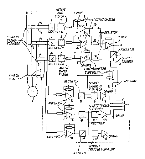
The circuit for the electronic overcurrent tripping
device shown in the drawing is used for controlling a motor
connected to a 3-phase grid RST via the switchgear 2. Current
transformers 3, 4, 5 are used for sensing the current through
the grid lines signals corresponding to the current IR, IS, IT.
The transformer outputs, as well as the voltages UR, US, UT are
fed to multiplier circuits 6, which in response generate signals
~
- - \
~ 9 20365-2727
corresponding to the instantaneous powers delivered by of the
individual phases. In the steady state condition, these
signals have a sinusoidal wave form with a DC component corres-
ponding to the active power, and a frequency equal to twice the
grid frequency. Changes in the load or short circuits can
cause signals with frequencies other than zero or twice the
grid frequency during such state changes, the content of the
transient can become so large that the operative range of the
subject circuit can be exceeded. Therefore, the signals from
the multipliers are fed respectively to fourth-order active
band filters 7, the center (passing) frequency of which is
set at twice the grid frequency. The symmetrizing members 8
connected to these filters are feed-back operational amplifiers,
having potentiometers 9 in the feed-back path. Differences in
the phase powers of the unfaulted motor and grid asymmetries
can be compensated by adjustment of the potentiometers 9. The
individual powers are summed through resistors lO, and the sum
is applied to a further operational amplifier 11. The resultant
voltage from the amplifier ll may be output as shown. In
addition, rectifier 12 is connected to the amplifier output to
determine the mean value of the amplifier signal. The mean
value is fed to a Schmitt trigger circuit 13 which determines
when the mean value of the amplifier output exceeds a present
threshold level.
In measurements with shorted turns caused by taps
at the motor winding it has been found that even with several
shorted turns the amplitudes of currents and voltages have very
small differences. However~ the phase shifts between currents
and voltages change greatly. Under these conditions it can be
calculated that the output signal of the circuit is proportional
- -- 4 --
129~6~ 20365-2727
to 2 UI sin (~/2), whereby ~ the phase difference of the
winding with shorted turns to the windings without shorted turns
is. The evaluation circuit is therefore very phase-sensitive.
The phase sensitivity is necessary especially in the case of
shorted turns which result, as previously mentioned in currents
with nominal values. The evaluation method should indicate,
if possible, only one shorted turn. All normal operating
states should not be affected here.
A change from a no-load to full-load causes no
substantial changes of the total signal resulting from the
addition of the phase power signals although the instantaneous
powers of the individual phases become substantially larger.
- 4a -
. .
il
1 This, however, is not the case when the motor is initially `
2 switched on. The reason for this is that the contacts of the
3 switch do not close completely simultaneously and the transient
4 behavior of the three-phase windings is not identical. In
order to compensate for this effect, the signal coming from the
, 6 Schmitt trigger 13 is therefore fed to a time delay circuit 14-
7 the output of which is connected to an AND gate 15. A second
8 input of the AND gate is connected to the output of the Schmitt
g trigger circuit 13. From the AND gate 15, a tripping signal is
sent to the switchgear 2 if both conditions are met thereby
11 opening the switchgear. For picking-up short circuits serve,
12 as is well-known, integrating amplifiers 16 connected to the
13 current transformers 3 to 5 as a lowpass filter which are
14 connected via rectifiers 17 to a Schmitt trigger and flip-flop
circuit 18, and act on operational amplifiers 19. The output
16 ~of the operational amplifiers again are put to the tripping of
17 the switchgear 2.
L8 If a shorted turn occurs, the output signal has
19 reached its final value not more than 10 milliseconds later.
The reason for this high speed is the lack of, for instance,
21 integrating elements such as are used for the determination of
22 r.m.s. values or the like. The only delayed element in the
23 ;formation of the shorted-turn signal is the bandpass 7 which
24 follows the state change with a delay of 10 milliseconds.
Obviously, numerous modifications may be made to this
26 invention without departing from its scope as defined in the
27 appended claims.
28
29
-5