Note: Descriptions are shown in the official language in which they were submitted.
~29972~
1.
ELECTRO-OPTIC SWITCHING DEVICES
USING FERROELECTRIC LIQUID CRYSTALS
~AC~GROUND OF THE INVENTION
1. Field of Invention
This application relates to liquid crystal
electro-optical switching devices and, more
particularly, relates to electro-optical switching
devices employing ferroelectric liguid crystals.
2. Description of the Prior Art
The manipulation of light (electromagnetic
radiation in the infrared, visible, and ultraviolet
spectral regions) is becoming an important
information handling technology. The construction
of integrated optical cizcuits and the transmission
of information along optical fibers are particularly
attractive means for exploiting the information
carrying capacity of light. A variety of devices,
particularly for the generation and detection of
intensity modulated light, have been developed for
fiber and integrated optic systems. However, the
development of complete optical systems has been
hindered by the lack of suitable electro-optic (EO)
switches for manipulating incident light by the
application of electrical signals. Prior art EO
switches are made from any material by which the
intensityr polarization, or direction of the light
can be electrically controlled, but the ease with
which the~molecular orientation and hence refractive
index of liquid crystals ~LCs) can be manipulated by
applied electric fields has led to the development
of liquid crystal electro-optic switching devices
which exhibit improved light manipulating
characteristics.
These electro-optic switching devices of
the prior art have exploited a variety of
electrically-induced molecular reorientation effects
in nematic and chiral smectic liquid crystal phases,
as will be described below.
The electro-optic ef~ects in LCs result
from electrical and optical anisotropies of the LC
phases which in turn result from molecular
ordering. In nematic liquid crystals (hereinafter
referred to as nematics), the molecules tend to
orient so that their average symmetry axes are
parallel to a locally common direction. This
direction defines the unit director field ~,. (Note
that ~ is commonly written herein and in the art as
a vector, but since there is no physical
significance attached to its sign, that is ~, and
-~, describe the same physical states, ~, can be
represented as a line segment.) Besides this
orientational order, nematics are much like ordinary
liquids. A consequence o~ this orientational order
is anisotropy of the dielectric properties of
nematics. Namely, although a linear relationship
= E~ still exists between the electric and
displacement fields within a nematic, the dielectric
constant r is a second rank tensor. This causes the
~2~72~
free energy of a nematic in an externally applied
electric field to depend on its director
orientation. If the director is not otherwise
oonstrained, it will rotate to the orientation that
minimi2es the nematic's electrical free energy.
Since the dielectric anisotropy extends to optical
frequencies, this electrically-induced rearientation
produces an electro-optic effect that may be
exploited in practical light modulation devices.
The usual method for applying electric
fields in these devices is to place the LC between
closely-spaced parallel electrode plates. In this
geometry, voltage applied across the plates produces
an electric field perpendicular to the plates.
Since the electrostatic energy
W = 8
does not depend on the sign of E, this geometry
allows only one field-preferred optical state. This
state will have
n ll ~ if ~ > 0, or n 1 ~ if ~E < 0
where
~ E = 1: -- E
is the difference between the principal values of E
along axes parallel and perpendicular to ~,
respectively.
Since to be useful a device must have more
than one optical state, some means must be found to
prefer a director orientation other than the one
preferred by the field. This is usually
accomplished by treating the surface of the
electrode plates such that they prefer a di~ferent
orientation. Then, the applied field produces
elastic strain in the orientation of ~. When the
electric ~ield is removed, the stress resulting ~rom
that strain causes the orientation to relax back to
that preferred by the surfaces. This means of
operation has several consequences for the dynamic
characteristics of such devices. For instance,
while the turn-on time of such a device can be made
arbitrarily short by increasing the applied electric
field strength, the turn-off time is determined
solely by geometrical size of the device, and may be
undesirably long.
Over the past several years, another class
of liquid crystals, ferroelectric liquid crystals
(FL~s), has been developed. FLCs have the
orientational order characteristic of nematics, as
described above, and in addition have their
molecules arranged in layers so that their ~ass
density is quasiperiodic in one direction. Layered
LC phases are called smectic phases. In smectic LCs
(as opposed to ordinary solids) the distribution of
the molecules within the layers is somewhat liquid
in nature. The prerequisites for ferroelectricity
occuring in smectics are that: (1) the constituent
molecules must be chiral, in other words not
superimposable on their mirror images; and (2)
must be tilted from the direction normal to the
layer surfaces. When these conditions are met, the
LC will have a spontaneous ferroelectric
polarization P even in the absence of an applied
electric field, as pointed out by Meyer et al. in Le
Journal de Ph~sique, Volume 36, pages L69-71, March,
1975.
s
The geometrical relationships between the
layers of ferroelectric liquid crystals in the
chiral tilted ~mectic phase, ~, and P are ~hown in
FIGURE 1. In FIGU~E 1, the smectic layer planes are
parallel to the X-Y plane and perpendicular to the
z-axis. The director ~ in its preferred orientation
tilts away from the z-axis by the angle ~O. In
addition, the projection of ~ onto the layer plane
X-Y defines the "c-director" c, which makes an angle
~ to the y-axis. Finally, the permanent
polarization P is in the plane of the layers and
perpendicular to ~ (i.e., ~ = POZ x n ), that is,
it is perpendicular to ~, making the angle ~ to the
x-axis.
The displacement field D in FLCs has a
dielectric part linearly proportional to E, similar
to that described above in nematics, but in addition
has a permanently nonzero part resulting from the
spontaneous polarization P. Thus, the electrostatic
free energy of FLCs has a part which is quadratic in
E like nematics, and a part linear in E,
proportional to -~ E. The FLC seeks to orient its
director so as to minimize the total free energy
within its thermodynamic constraints, which
constraints essentially fix the tilt angle ~O. Flow
involving changes in the direction of the layering
is extremely dissipative, however, leaving changes
in the azimuthal angle ~ as the principal means
available to the FLC to minimize its free energy.
The inclusion of a tecm proportional to ~ makes
this energy depend on the sign of an applied
electric field. Thus, practical devices can be made
in the above-mentioned parallel plate geometry where
two optically distinct states may be selected by
voltages of opposite sign applied to the plates.
This allows both the turn-ff and turn-on times of
such a device to be made shorter by increasing the
applied field strength.
The dielectric anisotropy of both nematics
and FLCs results in them being optically aniso-
tropic, with the nematics being uniaxial and the
FLCs being biaxial, but with refractive indices
along the two axes perpendicular to ~ typically
nearly equal, so that for most purposes FLCs are
considered to be optically uniaxial, with the optic
axis along the director ~ as in nematics. Thus, in
either case, electrically induced orientation
changes produce changes in refractive index, and
these electro-optic effects may be exploited for
practical devices, despite the substantial
differences in the geometry of the optic axis and
applied field directions.
One class of such devices makes use of
the change in polarized light passing through an
"optically thick" slab of LC material. sy
"optically thick" is meant that Qnd is comparable or
larger than ~, where ~n is the LC refractive index
anisotropy (birefringence), d is the slab thickness,
and ~ is the light's vacuum wavelength. The twisted
nematic, supertwisted birefringence effect, nematic
~-cell, and variable birefringence nematic devices
all fall in this class, as does the family of
surface-stabilized FLC (SSFLC) devices proposed by
N. Clark and S. Lagerwall in U.S. Patent No. 4,563,059.
These devices operate best when the light they are
modulating is incident in a direction near to the
normal of the slab. Typically,such a device is placed
between a crossed polarizer and analyzer,and it operates so
that in one state the transmitted output light is
~reatly attenuated in intensity by being mostly if
not completely absorbed in the analyzer, whereas in
the other state the output light is transmitted with
as much of the incident intensity as is practical.
In neither state does the direction oF the incident
light propagation change upon crossing the LC
layer. Of course, variations are possible where
reflective materials are incorporated into such
devices such that the incident light is returned
toward its source after two passes through the LC
slab, but the basic action is still as described
above.
- Another class of such devices relies on the
reflection and refraction properties of light at an
interface between two dissimilar dielectrics, one of
which is an LC. Examples in the prior art of this
class of devices using nematic LCs are disclosed in
V.S. Patent Nos. 4,201,442 and 4,278,327 by D.H~
McMahon and R.A. Soref and U.S. Patent No. 4,385,799
to Soref. Also, as taught by Kashnow and Stein in
Applied Optics, Vol. 12, No. 10, October, 1973,
electrooptic effects have been achieved by placing a
thin nematic liquid crystal layer between two glass
prisms of appropriate refractive index. Eor a range
of angles of incidence oE light on the prism-liquid
crystal interface, the light is partially
transmitted or totally reflected, depending upon the
electric field controlled orientation of the optic
axis in the nematic layer. Furthermore, as
' disclosed by Terui and Kobayashi in Proceedings of
the SPIE, Vol. 517, p. 267 (1984), the light need
not propagate through the FLC medium itsel~ Çor this
type of switching to work, for the same total
internal reflection phenomena is obtained where the
LC material merely forms the "cladding" for a
waveguide of some higher index material. The e
inventions thus relate to electro-optic devices for
switching input light more or less completely
between two or more outputs. They separate the
outputs by changing the direction of the input light
by reflection at an interface between a nematic LC
and another dielectric. Consequently, they teach
that by selectively applying electric fields to the
nematic LC, the direction of the output light may be
selected.
SUM~IARY OF THE INVENTION
In this application, new ferroelectric
liquid crystal devices of the general type outlined
above are described which differ from the SSFLC and
similar devices in that the causative electro-
optical effects occur at the interface between the
FLC and another dielectric material and that the
length of the optical path through the PLC is not of
primary importance.
According to the present invention, first
and second dielectrics define a boundary, where at
least one of the dielectrics is FLC material.
Electric fields applied to the FLC can switch the
FLC between different orientations. Light is then
directed toward the boundary in such a way that the
manner in which it interacts with the boundary is
dependent upon the orientation of the FLC.
The devices of the present invention are
divided into two categories, based on whether they
function principally by effecting changes in the
complex amplitudes of the reflected and refracted
rays or by changing the direction of the refracted
rays.
A first embodiment of an amplitude changing
device contains a dielectric-FLC interface in which
the FLC's index of refraction at the interface i5
changed by reorienting the molecules within the
smectic layers of the FLC. A voltage pulse is
supplied to select one of the states such that
either the reflected or refracted intensity produced
by the FLC has a large ratio to the similar
intensity produced by another ~LC state selected by
a different applied voltage pulse. Thus, a switch
can be made similar to the nematic liquid crystal
switching devices of the prior art except that
ferroelectric liquid crystals are used so as to take
advantage of their more rapid switching capabilities
and intrinsic "memory".
By preparing the smectic layers at a
certain angle to the interface between the
dielectric and the FLC, an embodiment of an
amplitude changing device may be produced which has
optical states similar to those in the nematic
devices of U.S. Patent Nos. 4,201,442, 4,278,327,
and 4,385,799 noted in the Background of the
Invention. In other words, the applied field
selects either a first state with ~ perpendicular to
the interface, wherein incident light of a first
polarization sees the refractive index ne while
light of another polarization sees refractive index
nO, or a second state with ~ parallel to the
interface and perpendicular to the plane of
incidence, wherein the light is affected in a manner
opposite to that in the first state. Due to the
geometry of the ferroelectric liquid crystal,
however, the electric field applied to the FLC must
be applied parallel to the interface, wherea~ in the
nematic devices of the prior art the electric field
is applied parallel to the normal to the plane.
In a ~econd embodiment of an amplitude
changing device, an interface may be formed between
two diEerently oriented FLC regions. In this
arrangement, appropriately polarized light sees
different indices of refraction on either side of
the interface depending upon the orientation of the
PLC molecules. This configuration may be used to
form a switch in which light propagating through the
FLC slab is either transmitted across the boundary
between the regions or is totally internally
reflected at the boundary depending upon the field
selected director states of the two regions. In
addition, this type of switching may work if the FLC
material merely forms the cladding for a waveguide
of a higher index material, wherein the index of
refraction of the cladding can be changed with
applied voltage pulses so as to change the optical
path of the light propagating through the waveguide.
In a third em~odiment of an amplitude
changing device, the FLC exhibits an inhomogeneous
director configuration. Namely, if the FLC's
interaction with the interface prefers an
orientation that presents a first refractive index
to incident light, when an electric field is applied
that prefers a different director orientation it is
possible that the director orientation will vary
from that preferred by the interface in the region
immediately adjacent to the interface to that
preferred by the applied field some distance away
from the interface, giving that region a second
refractive index. When the interface-preferred
orientation is one with low refractive index, the
~2~
11
portion of light transmitted across the interface
can be continuously increased by increasing the
applied electric field strength. When the interface
has a preferred molecular orientation that gives
large refractive inde~ to appropriately polarized
incident light, on the other hand, at a low applied
field that light will be initially transmitted.
However, as the light propagates through the ~LCI
the FLC's director orientation gradually changes,
and the polarization of the transmitted light nearly
follows along with ~. When the electric field
strength is increased, the distance over which the
director reorientation takes place is shortened, and
the above "following along" no longer occurs,
allowing the transmitted intensity to be
continuously reduced.
The FLC optical switching device of the
present invention also performs switching functions
by causing electrically-induced changes in the
molecular orientation so as to change the
propagation direction of the transmitted light.
Appropriately polarized light is refracted at the
interface in diferent directions which depend on
which FLC molecular orientation has been selected by
applied electric fields.
The switching function of the present
invention may also be controlled solely by light
such that an external electrical power source is not
necessary. The presence of light is sensed by a
photovoltaic device, and an output voltage is
generated which is sufficient to drive the switching
of the optical switch.
It was previously envisioned that the
selective reflection properties of liquid crystals
of other "textures" of the liquid crystal slab (such
~ 2~
.L
12
as twisted, homeotropic, scattering, etc.) and
possibly other mesophases lcholestic or smectic)
could be used for electro-optic switching by Soref
in his article entitled "Liquid Crystal Switching
Components," Fiber Optic Communications, Vol. 21,
1980, pp. 1-5; however, FLCs of the type disclosed
herein have not been used previously in electro-
optic switching devices. Due to the substantial
geometrical differences between the nematic and
smectic liquid crystals, the same switching
technique used for nematic crystals as disclosed by
Soref cannot be used for smectic liquid crystals.
These geometric differences are particularly
important, for the improved switching
characteristics of the FLCs over the nematic LCs are
an unexpected advance in the art of electro-optic
switching.
The devices of the type used in the present
invention differ from those of the above-mentioned
prior art in several ways. First, although the
present invention uses PLCs, the present invention
differs from the family of FLC devices previously
proposed by Clark and Lagerwall, for in the Clark-
Lagerwall devices noted above, a beam or ray of
polarized light is transmitted through an optically
thick slab of FLC, and emerges propagating in
approximately the same direction as its incident
direction. By applying electric fields to the FLC
slab, the intensity of the polarization components
of the transmitted light beam can be varied. These
variations can then be used to effect changes in the
total intensity of the beam by passing it through a
polarization analyzer. In contrast, in the devices
of the present invention, a beam of light is
incident on an interface between an FLC and another
~2~2~
13
dielectric, where it is reflected and refracted. By
applying electric fields to the FLC., either the
relative intensities of the reflected and re~racted
beams can be changed, or the direction of
propagation of the refracted beam can be changed.
Second, although the present invention
relies on the effect on light of an interface
between an LC and another dielectric, they differ
from those devices where the LC is a nematic. In
those devices using nematics, an electric field E
applied across the nematic slab produces a rotation
of the director about an axis perpendicular to
itself and the electric field. Since the
electrically induced torque does not depend on the
sign of E, only one electrically-selected director
orientation is possible, that is, one with
parallel to ~ for ~ > 0 and that with ~
perpendicular to E for ~ < 0. A device with more
than one state must then use some other efect,
usually surface forces, to favor some other director
orientation. In the devices of the present
invention, however, the geometry is quite different,
reflecting the different underlying symmetry of the
FLC. The director reorientation is on a cone of
angle ~O whose axis is normal to the smectic layer
planes, the so-called "tilt-cone." Applied electric
fields produce changes in the azimuth of the
director on this cone, and in general, the field-
preferred orientation has P parallel to the
component of E that lies parallel to the layer
plane.
Although more general configurations are
within the scope of this invention as will be
described below, a simple example serves to
3s illustrate the differences between FLC and nematic
14
LC dielectric interface devices. If the smectic
lay~rs are oriented normal to the surface of the FLC
slab, for example, an electric field E applied
across the slab will prefer according to its sign
5 one of two director orientations, both parallel to
the slab surface, but differing in orientation by
2~o. Thus, the effective rotation is abo~t an axis
perpendicular to ~ but parallel to E, with two
field-preferred director orientations, both
perpendicular to E.
These differences between the devices of
the present invention and those of the prior art
result in many significant advantages for the
devices of the present invention. They offer the
ability to change the intensity or direction of a
light beam without the use of a light absorbing
polarizer or analyzer. They work equally well with
input light of different wavelengths. Further, they
can switch input light between two or more outputs
on the basis of light beam propagation direction,
which is advantageous in many applications.
Finally, by having a stronger, sign-dependent
coupling to applied electric fields, they overcome
the disadvantageous slow response times of nematics,
particularly in response to the removal of the
applied field.
BRIEF DESCRIPTION OF THE DRAWINGS
These and other objects and advantages of
the invention will become more apparent and more
readily appreciated from the following detailed
description of the presently preferred exemplary
embodiments of the invention taken in conjunction
with the accompanying drawings, of which:
FIGURE l is a schematic representation of
the geometry of the smectic C liquid crystal
material;
FIGURE 2 is a schematic r~presentation of
the general geometry of reflection and refraction at
an interface between anisotropic media;
FIGURES 3a - 3d are schematic
representations of an FLC dielectric interface with
director states presenting low and high refractive
indices to polarized incident light;
FIGURES 4a - 4d are schematic
representations of a single-pass FLC switch in which
the FLC is a thin slab between two glass prisms;
FIGU~ES 5a and 5b are schematic
representations of a double-pass FLC switch which is
insensitive to the polarization of the incoming
light;
FIGURE 6 is a schematic representation of
an FLC l-input, 4-output switch;
FIGURES 7a - 7d are schematic
representations of a dielectric-FLC interface with
smectic layers at an angle ~ to the interface such
that in a first state the molecules are oriented
parallel to the normal to the interface and such
that in a second state the molecules are parallel to
the interface;
FIGURES 8a - 8c are schematic
representations of a switching device in which light
is incident from a waveguide and may be switched
from one waveguide to another;
FIGURES 9a - 9c are schematic
representations of a switch with an FLC-FLC
interface;
FIGURE 10 is a schematic representation of
a matrix switch with a plurality of the FLC-FLC
~.2~
16
interfaces shown with reference to FIGURE 9 arranged
such that incoming light may be selectively routed
to one of a plurality of optical outputs;
FIGURE 11 is a schematic representation of
a waveguide switch utilizing the FLC-FLC interface
shown with reference to FIGURE 9;
FIGURES 12a and 12b are schematic
representations of a dielectric-FLC interface with a
smectic layer orientation as in FIGURE 3 but
exhibiting an inhomogeneous FLC orientation such
that transmitted and reflected light intensities may
be controlled in a continuous method;
FIGURES 13a and 13b are schematic
representations of a dielectric-FLC interface as in
FIGURE 12 but with a different preferred molecular
orientation at the surface in which incident light
is transmitted across the interface and follows the
director orientation in the absence oE a strong
applied field;
FIGURES 14a and 14b are schematic
representations of a dielectric-FLC interface
employing a direction changing feature in which
incident light is refracted in two different
directions by the two different director
orientations selected by applying opposite fields
parallel to the x-axis;
FIGURE 15 is a schematic representation of
the direction changing principle shown with
reference to FIGURE 14 which occurs at an FLC-FLC
interface:
FIGURES 16a and 16b are schematic
representations of direction changing devices
exploiting the direction changing principal shown
with reference to FIGURE 14;
17
~IGURE 1~ is a schematic representation of
an FLC cell of the preferred embodiment of the
present invention;
FIGURE 18 is a schematic representation of
a means for producing alignment of the smectic
layers of applying a shear strain to the PLC; and
FIGUR~S l9a and l9b are schematic
representations of devices for producing the
switching voltages used by the FLC from incident
light.
DETAILED DESCRIP~ION OF THE PREFERRED EM~ODIMENTS
FIGURE 2 shows a ray of light with wave
vector ki incident on the interface between two
anisotropic materials, medium A and medium B. The
incident light wave vector ki makes an angle ~i with
a normal to the interface and forms two reflected
rays with wave vectors krl and kr2 at angles ~rl and
~r2 to the normal, respectively. Incident light
also forms two refracted rays with wave vectors k
and kt2, at angles ~tl and t2 to the normal to the
interface, respectively. The complex amplitude
(intensity and polarization state), direction, and
phase of the rays depend on the refractive indices
of mediums A and B. The present invention uses
these properties to make practical light switching
devices by allowing light to be incident on the
interface between the region filled with one
dielectric material (either an FLC or some other
material) and a region filled with FLC. Then,
almost any change in the FLC's molecular orientation
immediately adjacent to the interface will produce
changes in its reflection and refraction
properties. Methods for producing such molecular
gL2~972~
18
reorientations in FLCs by applying electric fields
that change in strength and direction to the region
that contains the PLC are known in the art; for
example, a multitude of molecular orientation states
that can be produced and stabilized between parallel
plates are disclosed in U.S. Patents 4,367,924 and
4,563,059 to N. Clark and S. Lagerwall. However,
the present invention operates much faster than the
nematic switching devices of the prior art.
Furthermore, the present invention can be arranged
more advantageously than surface stabilized
ferroelectric liquid crystal switching devices as
described above.
The devices of the present invention are
divided into two categories, based on whether they
function principally by effecting changes in the
amplitudes of the reflected and refracted rays or by
changing the direction of the refracted rays. Each
of these devices and their corresponding geometries
will be discussed in Section I below, and then, the
method of constructing the presently preferred
embodiment incorporating the switching geometries
discussed in Section I will be described in Section
II.
I. FLC GEOMETRIC ORIENTATION FOR EO DEVICES
A. Amplit ~
The amplitude changing devices of the
present invention are of two types: those in which
applied voltage steps and pulses select between
discrete, different molecular orientation states,
and those in which continuous changes in the applied
field produce continuous changes in the molecular
orientation. Devices of the first type have more
~2~
19
than one discrete light amplitude state, each being
associated with a discrete director orientation
state. The differences between the director
orientations of the different states persist to
within a distance from the interface which is small
compared to the light's wavelength. Devices of the
second type, on the other hand, have a continuum of
amplitude states arising from continuously varying
director states produced by continuously varying
applied electric field strength. The greatest rate
of light amplitude change in these devices is
produced when the director changes from a surface-
favored orientation immediately adjacent to the
interface to a field-favored orientation over a
length comparable to the light's wavelength. Each
oE these devices exhibits characteristic features
which are advantageous for selected functlons as
will be described below.
l. Discrete-state devices
-
a. Dielectric-FLC interface with
electric fields applied perpendicular
to the interface
In general, any molecular orientation
change in an FLC will produce some changes in the
intensities of light rays reflected and refracted at
the interface between the Fl,C and another dielectric
material; however, the present invention is directed
to those configurations where either the reflected
or the refracted intensity produced by the FLC
molecular orientation selected by an applied voltage
has a large ratio compared to the similar intensity
produced by the FLC states selected by a different
~299~1
2~
applied voltage. In factl a virtually infinite
ratio o intensities can be achieved by exploiting
the phenomenon of "total internal reflection" in
which a ray of light propagating through a medium of
larger refractive index and incident on an interface
with a medium of lesser refractive index is totally
reflected. This occurs when the angle of incidence
is increased beyond the critical angle, that angle
at which either the refracted ray or its wavefront
normal is parallel to the interface. Thus, for
angles of incidence larger than this critical angle
the incident ray is entirely re1ected, and the
refracted intensity is zero.
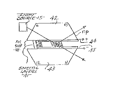
FIGURES 3a-3d show a first embodiment in
which a ray of light from a light source 15 (which
may be freely propagating or confined to an optical
fiber guide or other type of waveguide) incident
through a dielectric medium of a first refractive
index nl strikes the interface with a region
containing FLC material. The coordinate system is
chosen such that the z-axis is perpendicular to the
interface defined by the X-Y plane, the x-axis is
perpendicular to the plane of incidence, and the y-
axis is perpendicular to both the x and z axes.
In this embodiment, the smectic layers of
the FLC are oriented so that their intersections
with the plane of the interface (the X-Y plane) make
an angle ~ to the y-axis and are tilted away from
being normal to the interface by an angle ~.
Different director orientations can be selected by
applying an electric field E o~ the appropriate
direction and sign. For instance, an electric field
perpendicular to the interface can be applied by
applying a ~oltage across a transparent electrically
conducting coating on the face of the first
12~
dielectric medium and an electrically conducting
plate that bounds the FLC region parallel to the
above-mentioned interface. IA more detailed
structure of the ~LC and the electrodes will be
given below with reference to FIG~RE 17.~ The
preferred director orientation has its P parallel to
that component of the applied field E that is
parallel to the layers, and reversing the applied
voltage changes the sign of E such that it prefers a
director orientation at an angle 2~o with respect to
the other orientation.
Whichever orientation is preferred will
persist at least to within a length ~ of the
interface, where ~ is the length that characterizes
the size of a distortion whose elastic energy
density K/~2 is equal to the electrostatic energy
density PE~ [K/PE~2). For strong applied fields
E >> K/(P~) , this distance will be small compared
to the light wavelength ~ and will have
substantially no effect on the device operation.
Selection of other director orientations besides the
field-preferred ones are possible through the
mechanisms of surface stabilization disclosed by
Clark and Lagerwall in U.S. Patent Nos. 4,367,924
and 4,563,059. As they disclose, in the absence of
strong applied fields, up to four distinct director
orientations may be stabilized by the FLC's
interaction with the surface, and switching between
these director orientation states may be
accomplished by stronger electric fields applied
normal to the surface for limited times. Thus,
there exists the possibility for six field-selected
director orientation states near the interface: the
two states preferred by strong fields applied normal
to the interface but oppositely directed, and the
22
four surface-stabllized states that can be ~witched
between by the applied field pulses as disclosed by
Clark and Lagerwall.
In general, linearly polarized light
incident from the first dielectric on its interface
with the FLC of a given director orientation will be
partially reflected and partially transmitted. The
partially transmitted light will, in general,
consist of two rays, the ordinary and the
extraordinary rays. If the first medium is an
isotropic dielectric, the partially reflected light
will consist of oniy one ray, altho~gh, in general,
it will now be elliptically polarized. If the first
medium is also anisotropic, however, the partially
reflected light will, in general, consist of two
rays, one ordinary and one extraordinary. The
ellipticity of the reflected ray (in the case where
the first medium is isotropic) and the amplitudes
and intensities of all the reflected and transmitted
rays (whether the first medium is isotropic or
anisotropic) will differ between the various
director states selected by applied electric fields
normal to the interface.
If, however, the angle of incidence ~i is
larger than the critical angle ~c for the
transmitted ordinary ray, the only transmitted ray
will be the extraordinary one. This, rather than
the reverse, is the case possible for FLCs since
they have an extraordinary refractive index ne
greater than an ordinary refractive index nO 50 that
the refractive index seen by the extraordinary ray
is always greater than the refractive index seen by
the ordinary ray which is identioally nO. The
refractive index seen by the extraordinary ray,
however, depends on its orientation relative to the
23
optic axis or director of the FLC. The closer it-
~wave propagation direction (the direction normal to
its wavefronts) is to the FLC's optical axi~, the
more nearly the refractive index seen by the
extraordinary ray approaches nO. This relative
propagation direction will, in general, be different
for the various field-selected director states,
thereby implying that the extraordinary transmitted
ray sees a different refractive index for these
states. Thus, the refractive index nl of the first
medium and the angle of incidence can be further
arranged, without losing the property of not
transmitting the ordinary ray, to transmit an
extraordinary ray in one of the director states and
to totally internally reflect all the incident light
for another director state. Thus, voltages applied
across the two above-mentioned electrodes boundiny
the FLC medium can select between two director
states, one with the director orientation for which
the extraordinary transmitted ray sees a higher
refractive index and in which some light is
transmitted across the interface (the "transmitting
state"), as shown in FIGURE 3a, and one with the
director orientation more nearly parallel to the y-
axis giving a lower refractive index so that all theincident light is reflected and none is transmitted
(the "reflecting state"), as shown in FIGURE 3c.
Consequently, a switching effect can be achieved
similar to that using nematic LCs as disclosed b
R.A. Kashnow and C.R. Stein in Applied Optics,
Volume 10, pages 2309-2311, October, lg73 and in
U.S. Patent Nos. 4,278,327 to McMahon and Soref and
4,3a5,799 to Soref.
Achieving the largest possible refractive
index change between the director orientations of
~L2~
2~
the transmitting state and the reflecting state
allows the largest angle of incidence while at the
same time making the oper~tion o~ the device least
sensitive to changes in the angle of incidence.
Large refractive index changes are obtained by using
FLC materials with large birefringences ~ An ' s ) and
large tilt angles (~O's), and orienting the smectic
layers to have small tilts (b's). For the special
case of ~=0, the field-preferred director states
will be parallel to the interface, allowing incident
light polarized perpendicular to the plane of
incidence (hereinafter referred to as s-polarized)
to be affected by the full extraordinary index ne
for one of the field-preferred director states
obtained when = ~O . The refractive index seen by
s-polarized incident light for the other field-
preferred director state is made smaller the
larger ~O is, reaching a minimum value of nO
when ~O = 45.
A schematic diagram of an embodiment of a
single-pass switch using ferroelectric liquid
crystals of the smectic phase is shown in FIGURES 4a
- 4d. The switch is formed by a thin slab of an FLC
material 40 containing smectic layers 41 between two
glass prisms 42 and 43 with transparent electrically
conductive coatings 44 and 45 on their respective
faces. Voltages pulses are applied to these
coatings to select between the different possible
director orientations. The orientation of the
layers, the angle of incidence, and the refractive
index np of the prisms are arranged so that for the
director state selected in FIGURE 4c a light ray
incident from source 15 on port 11 of prism 42 sees,
regardless of its polarization state, a refractive
index less than npsin9i at the FLC interface, and is
~2~
therefore totally internally reflected to exit out
port 13 of prism 42. ~owever, when another director
state is selected, as shown in FIGURE 4a, the
polarization component of a ray incident through
port ll that excites the extraordinary mode of
propagation in the FLC will no longer be totally
internally reflected since it sees a refractive
index large enough (i.e. > npsin~i) to make the
angle of incidence smaller than the critical
angle. Thus, part of this ray is transmitted across
the FLC slab and exits through port 14 of prism 43,
while the other part is reflected and exits through
port 13 of prism 42 as before. The portion of the
incident light that is transmitted in this state can
be maximized by matching the refractive index seen
by the extraordinary ray in the FLC to the
refractive index seen in the prism by the ray that
excites the extraordinary ray in the FLC by suitable
choice of the prisms' material. Any of the four
ports ll, 12, 13 and 14 may be used as the incident
port for the light ray, and more than one may be
used simultaneously.
When the above-mentioned refractive index
matching condition is satisfied, the embodi~ent of
FIGURES 4c and 4d acts as a polarizing beam
.splitter, substantially completely separatiny out
the two orthogonal linear polarization components
that make up an incident light ray of arbitrary
polarization state by transmitting the one that
excites the extraordinary mode while reflecting the
other. This property enables further novel and
useful light switching embodiments. Foc example, if
the light output from a single-pass FLC switch as
shown in FIGURES 4a-4d is redirected to be incident
on another similar switch, an optical switch results
26
that will completely switch unpolarized input
light. An embodiment of such a switch using FLCs is
shown in FIGURES 5a and 5b.
FIGURES 5a and 5b show an embodiment of a
double-pass FLC switch combining two of the elements
of FIG~E 4 with retarders 50 and 51 so as to make
the switch substantially insensitive to the
polarization of the incident light. The switch in
FIGURES 5a and 5b is also formed by a thin slab 40
of FLC material between two prisms 42 and 43, and
the configuration of the FLC-glass interface is the
same as described above with reference to FIGURES
4a-4d. Since the switch described above with
reference to FIGURES 4a-4d can only switch that
polarization of the incident light that excites the
extraordinary mode of propagation in the FLC,
however, the switching device of FIGURES 5a and 5b
employs retarders 50 and 51 which change the
polarization state of polarized light passing
through them. These retarders may be plates of a
birefringent material (waveplates) or may operate by
use of the retardation experienced by a light ray
upon total internal reflection as is exploited in a
device known in the art as the Fresnel rhomb.
FIGURE Sa shows such a switch when the
applied voltage has selected the FLC state in which
the component of the incldent light that excites the
extraordinary mode is substantially totally
transmitted. An unpolarized input ray from light
source 15 comprised of two orthogonally polarized
components enters through port 11 and strikes the
prism-FLC interface at an angle of incidence greater
than ~c for the component that excites the ordinary
mode in the FLC. This polarization component of the
incident ray is thus totally internally reflected
~L2~9~L
27
and stays within the same prism 42. The other
component, on the other hand, is transmitted without
substantial reflection through the FLC reglon 40
into the other prism 43 since it sees the same
S reractive index in the prism and in the FLC. ~oth
light components are then totally internally
reflected at the air-glass interface, and are
directed back from opposite sides towards the FLC-
prism interface. Each light component then passes
through a retarder (either 50 or 51). Retarder 50
converts the polarization of the reflected light
into the state that excites the extraordinary mode
in the FLC so that on its next pass towards the FLC
prism interface it is substantially totally
transmitted, while retarder 51 converts the
polarization of the transmitted extraordinary light
- into the state that will be totally internally
reflected at the FLC-prism interface. In this
manner, the two components are recombined to travel
through the second glass prism 42 and exit through
port 14.
FIGURE 5b shows the double-pass FLC switch
when the applied voltage has selected another
molecular orientation. As shown, both light
components are totally internally reflected at the
FLC-glass interface and propagate within the first
glass region 42. Both components are again
reflected at the glass-air interface and pass
together through the retarder 50. Both components
continue to propagate towards the FLC-glass
interface where they are both again totally
internally reflected, and then they propagate back
through the glass prism 42 to exit through incident
port 13.
2B
The switch shown in FIGURES Sa and 5b may
also be used as a 4-port device having two .~tates.
For this purpose, incident light may be applied
through a second incident port such as port 12 of
the second glass region 43 at the same angle of
incidence as the light applied to incident port 11
of the first glass region 42. When the FLC
molecules are oriented such that unit director ~ is
further from the y-axis, both components of the
light incident at port 11 exit together through the
opposite port 14, and both components of the light
incident on the port 12 exit together through the
opposite port 13. When the unit director ~ of the
FLC is closer to the y-axis, on the other hand, both
components of the incident light stay in the glass
region from which they were incident. Thus, light
incident on port 11 exits through port 13, and light
incident on port 12 exits through port 14.
Consequently, this optical switch defines a 4-port
device with two states, one state in which port 11
is optically connected to port 13 and port 12 is
optically connected to port 14, and another state
where ports 11 and 14 and 12 and 13 are respectively
connected to each other.
The optical switching device o~ FIGURES 5a
and Sb thus function as a versatile optical routing
switch in which an input beam may be connected to
one of two voltage-selected outputs. In addition,
when the switch is in the transmitting state, by
choosing the retardation of the retarders 50 and Sl
to be different from that specified above, light
incident at port 11 can exit at both ports 13 and 14
in a ratio of intensities which is determined by the
retardation of the retarders.
~2~7;~
29
FIGURE 6.shows another embodiment in which
the same effect described above with reerence to
FIGURES 4a-4d can be used to make a 1 x N (1 input
routed to a chosen one of N outputs) switch. In
addition, the switch of FIGURE 6 can also work in
reverse as an N x 1 (chosen one of N inputs routed
to a single output~ switch. Furthermore, sets of
the 1 x N and N x 1 devices can be combined to make
an N x N switch where all N! possible connections
(where each input is connected to only one output
and each output is connected to only one input) are
voltage selectable. FIGURE 6, for example, shows a
l-input, 4-output switch where an input light ray
from light source 15 incident at port 11 can be sent
to any one of the four outputs 61a, 61b, 61c and 61d
by applying the appropciate voltage pulses between
electrodes 63a and 64a, 63b and 64b, 63c and 64c,
and 63d and 64d, respectively. As shown, the third
output has been chosen by applying an electric field
across electrodes 63c and 64c to select a different
director state than at the other electrode
locations. As a result, the molecules in the
portion of the FLC slab 40 between electrodes 63c
and 64c are oriented to give a high refractive index
such that the incident light is passed through the
FLC slab 40 to the second prism 42 and to the chosen
port 61c.
b. Dielectric-FLC interface with
electric field applied parallel to the
inter~ace
FIGURES 7a - 7d show another embodiment of
an FLC electro-optic switch in which the coordinate
system is chosen such that the FLC material occupies
~Z9~
the half-space region 2 ~ 0 and the X-Y plane is the
interface between the FLC and another diele~tric.
The smectic layer normal lies in the X-Z plane and
makes a nonzero angle ~ with the x-axis as ~hown in
FIGURE 7a. The Y-Z plane is chosen to be the plane
of incidence, and the incident light ray from light
source 15 makes an angle ~i with the z-axis as shown
in FIGURE 7b. If an electric field is applied
parallel to the y-axis, the FLC molecular
orientations selected by oppositely directed fields
both have their unit directors ~ in the X-Z plane.
One state will be more nearly parallel to the z-axis
as shown in FIGURE 7a, and the other state will be
more nearly parallel to the x-axis as shown in
FIGURE 7c. The most favorable configuration occurs
where the smectic C tilt angle ~O = 45, as is
found in some materials with an N to C phase
sequence, and where the layer normal also makes an
angle of 45 with both the x and z axes (i.e. ~ =
45). This configuration produces a device with
optical states like those in the nematic devices of
the prior art.
Namely, the smectic layers are oriented so
that an electric field applied parallel to the y-
axis selects either the state where X is parallelto the x-axis or the state where ~ .is parallel to
the z-axis depending on the sign of the electric
field. When the applied field selects the state
with ~ parallel to the z-axis, incident p-polarized
light sees a refractive index ne, while s-polarized
light sees a refractive index nO as shown in FIGURE
7b. However, when an oppositely directed electric
field is applied, the refractive indices seen by the
two orthogonal polarization components of the
incident light are interchanged such that p-
~29~7~
31
polari~ed light s~s refractive index nO and s-
polarized light sees refractive index ne as shown in
FIGURE 7d. Thus, a polarization insensitive 4 port
2 x 2 switch similar to the one described with
reference to FIGURES 5a and 5b can be constructed
even more simply since the retarders are no longer
needed.
The device of FIGURES 7a-7d works like a
nematic liquid crystal device of the prior art
except that when a FLC layer is used, the electric
field must be applied parallel to the plane of
incidence (parallel to the y-axis in FIGURES 7a-7d)
rather than being applied parallel to the normal to
the interface plane as for nematic liquid crystal
devices. The electric field may be applied parallel
to the interface plane by placing an arrangement of
interdigited electrodes along the interface between
the FLC layer and the dielectric. As in the other
embodiments, switching time is thus greatly reduced
over the devices of the prior art that use nematic
liquid crystals.
Switching devices of the type discussed
with reference to FIGURE 6 may also be constructed
using the configuration of FIGURES 7a-7d. Namely, 1
x N and N x N port devices may also be made by
arranging several such switches in a matrix.
c. Waveguide-FLC interface
FIGURES 8a - 8c show how the total internal
reflection effects described above can be exploited
in switching device where the light is incident erom
a waveguide. Here, the FLC slab separates two
waveguide structures fabricated into the bounding
plates. Electrodes fabricated at the waveguide-
~g972~
substrate interface or at the waveguide-FLC
interface allow voltages to be applled to control
the orientation of the FLC director~ The waveguide
is a high refractive-index material in which a
trapped beam can propagate as shown in FIGURE 8a if
the refractive indices o the FLC and substrate are
sufficiently low. The propagation can be viewed ~s
a multiple total internal reflection of the trapped
beam at the waveguide-FLC and waveguide-substrate
interfaces. The trapping of the light in the
waveguide can be controlled by the FLC orientation
by the same mechanism as discussed above with
reference to FIGURES 3 and 7. Switching the FLC so
that it presents an index of refraction higher than
that in the waveguide will allow the light to
radiate out of the waveguide, pass through the FLC
slab, and enter the waveguide on the other plate.
FIGURE 8a shows an FLC configuration
similar to that in FIGURE 3 where the high and low
index states are selected by electric fields applied
perpendicular to the substrates, while FIGURE 8b
shows a configuration similar to that in FIGURE 7
where the two states are selected by electric fields
applied parallel to the substrates. The fraction of
incident light energy that passes through the FLC
into the second waveguide will depend on the
geometry of the waveguide con~iguration, but almost
any structure having a significant waveguide overlap
will pass a signi~icant fraction (>5%) of the
incident light energy when the FLC is switched to
its high-index state, while the fraction of light
passed when the FLC is in its low-index state will
be much smaller. This waveguide-FLC waveguide
structure can be incorporated into a nonblocking N x
N routing switch as shown in FIGURE 8c, where the
12~2~L
33
FLC slab and waveguide layers are shown parallel to
the paper. The waveguide layers are patterned into
parallel channels oriented so that e~ch channel on
the top substrate crosses over every channel on the
bottom substrate. The electrodes are arranged so
that the FLC in each overlap area can be switched
independently. Then, light launched into one of the
channels on the top substrate can be coupled into
any chosen channel on the bottom plate by switching
the FLC where that top channel crosses the chosen
bottom channel. The dotted lines in the figure show
the path taken by the unswitched fraction of the
incident light, which is the same path taken by all
of the incident light when the FLC region is left in
its low-index state. The heavy solid lines show the
path taken by the light when the FLC is switched to
its high-index state.
Changes in the FLC orientation produce
changes only in its refractive index that affects
the extraordinary mode. Since for FLCs usually nO <
ne, the radiated light will always be extraordinary,
leaving the light that would excite the ordinary
mode in the FLC trapped within the waveguide. Thus,
the most efficient switching will be obtained if the
incident light is arranged to be largely of the
polarization that excites the extraordinary mode in
the FLC. This light radiates out of the guide most
strongly if the index it sees in the FLC is not too
much larger than that of the guide, i.e., if near
index-matching reduces reflections at the interface
in the light radiating state. Even i f the FLC index
is slightly less than that of the guide, the
evanescent wave of light propagating in a guide on
one substrate will couple to a propagating wave in
the guide on the other substrate if the FLC slab is
~997;;:~
34
thin enough, thus ~llowing this device to ~perate in
a mode where the indices presented by both field-
selected FLC states are less than that oE the guide,
but where one index is much less than that oE the
guide while the other index is only slightly less
than that of the guide.
d. FLC-FLC Interface
FIGURES 9a-9c show another embodiment of
the present invention in which light from light
source 15 is incident on the interface between two
differently oriented FLC regions. FIGURE 9a shows a
side view of an FLC device in accordance with the
present embodiment, whereas FIGURES 9b and 9c show
top views of the FLC devices.
As shown in FIGURE 9a, light propagates
through a thin FLC slab 81 which is bounded on both
sides by a low refractive index material 82 that
confines light by total internal reflection so as to
form a waveguide. On the surfaces of the bounding
media 82 are applied electrodes 83, 84, 85 and 86
which apply voltages such that a region of the FLC
is oriented either the same or differently from the
surrounding region. When the voltage applied to the
electrodes 83 and 84 (electrodes B3 and 84 being
disposed directly across from each other on
respective surfaces of bounding media 82) selects
the same FLC director orientation as is obtained in
the region of the slab defined by similarly disposed
electrodes 85 and 86, light incident on the
interface 87 between the two regions is transmitted
without change as shown in FIGURE 9b. However, when
the voltage applied to electrodes 33 and 84 selects
a different FLC director orientation than is
~:9~2~L
selected in the region defined by electrodes 85 and
86, an interface 87 between dissimilar dielectrics
is formed, at which the phenomenon Oe reflection and
refraction takes place as described above with
reference to FIGURE 2. Total internal reflection
will occur when the refractive index ni seen by the
incident light in the region defined by electrodes
85 and 86 is greater than the refractive index nt
that would be seen by light propagating parallel to
the interface but within the region defined by
electrodes 83 and 84 when the angle of incidence is
oblique enough (nisin~ > nt). For propagation of
light in optically anisotropic media such as FLCs,
the refractive index depends on the direction of
propagation of the light relative to the optic axis
(i.e., director) only for the extraordinary mode,
while the ordinary mode always sees the same
(ordinary) refractive index. Thus, switching at an
FLC-FLC interface can be obtained only for the
extraordinary part of the incident light, which sees
a lower refractive index the closer its propagation
direction is to the director.
For the director orientations shown in
FIGURE 9c, light propagating parallel to the
interface within the region defined by electrodes 83
and 84 is propagating closer to the director
orientation than the incident light in the region
defined by electrodes 85 and 86, so total internal
reflection is obtained for large enough angle of
incidence. The most favorable situation is the one
where the largest refractive index change can be
obtained, which occurs for FLC materials with large
tilt angle and layers oriented near to the interface
normal, as in the preparations reported by J.S.
Patel and J.W. Goodby in the Journal of Applied
~L2~72~L
3~
Physics, volume 59, pages 2355 2360, 1 April 1986.
~aving the smectic layers normal to the interface
has the further advantage for waveguide deviceR that
the applied field preferred states have their
directors and hence their optic axes parallel to the
cladding interface so as to allow the transverse
electric (TE) modes of the waveguide to be made up
purely of the extraordinary propagation mode,
thereby allowing the light incident on the interface
to be purely extraordinary and thus completely
switchable.
N x N switching devices may be constructed
by arranging several of the switching elements of
FIGURES 9a-9c in a matrix pattern as shown in FIGURE
l0. Each differently oriented FLC region 9l is
bounded by electrodes so that the applied field may
be selectively switched in order to orient the
director ~ either the same as or differently from
the surrounding region. In FIGURE l0, for example,
the dotted line shows the path taken when the
electrodes select the same director orientation as
in the surrounding region, whereas the dark lines
show the direction taken by the light when the
electrodes select a different director orientation
than the surrounding region.
Light does not need to propagate through
the FLC medium itself for the type of switching
shown in FIGURES 9a-9c and l0 to work. As noted by
Terui and Kobayashi in Proceedings of SPIE-The
International Society for Optical Engineering, Vol.
517, pages 267-274 ~l984), for example, the same
total internal reflection phenomena is obtained
where the liquid crystal material merely forms the
low index cladding for a waveguide of some higher
index material. A cross section of such a waveguide
97~
3~
switch is shown in FIG~R~ 11.
In the embodiment shown in FIGURE 11, light
propagates in the high-index waveguide layer which
i5 bordered on one side by a low index buffer layer
and on the other side by low index FLC material.
The effect of changing the director orientation in
the FLC layer on the evanescent fields of the light
propa~ating in the waveguide layer produces results
similar to those produced by the switch discussed
above with reference to FIGURES 8 and 9. Thus, each
of the types of devices described above may also be
constructed as a waveguide switch of the type shown
in FIGURE 11.
2. Continuous devices
~n Section I.l. above, it was assumed that
the FLC director orientation was everywhere the
same, specifically that ~ did not depend on the
normal to the boundary. However, it is well known
that there are ways to produce inhomogeneities in
the director orientation by making ~ depend on the
direction perpendicular to a surface that bounds the
FLC. For instance, the surface (the portion of the
FLC immediately adjacent the interface) may prefer
one sign of P s, where ~ is the outward surface
normal unit vector of the interface, and an applied
electric field or another nearby surface may prefer
the oppositely directed P. Thus, if the FLC layers
are oriented in this manner with respect to the
applied field, a region may be produced close to the
surface where the direction of P and hence ~ varies.
38
a. Case 1 - Surface-preferred ll
giving low refractive index
In the embodiment shown in FIGURES 3a - 3d,
the interface between the FLC and the other
dielectric may prefer the orientation of P that
gives a director orientation presenting low
refractive index to incident s-polarized light
(FIGURE 3d). If an electric field that prefers the
oppositely directed P is applied to the FLC when in
the orientation shown in FIGURE 3d, it is possible
that the director orientation will vary from that
preferred by the interface in the region immediately
adjacent the interface to that preferred by the
applied field some distance away from the
interface. In this manner, the "depth" ~ of the
interface may be varied. In fact, most of the
variation will take place within a distance ~ from
the interface, where:
~1~ - [K/(PE) ]2,
with K equal to the FLC's Oseen-Frank elastic
constant, P equal to the ferroelectric polarization
magnitude, and E equal to the strength of the
applied field.
Thus, for a low applied electric field ~ is
large, and the region close to the interface has the
orientation with a low refractive index for s-
polarized light so that total internal reflection
occurs as shown in FIG~RE 12a. As the applied
electric field is increased, ~ decreases, eventually
becoming comparable to the penetration depth of the
light's field into the FLC. At this point an
appreciable quantity of light starts being
~2~319 72~L
~9
transmitted as shawn in FIGU~E 12b. Further
increases in the applied electric field cause
further decreases in ~, thereby causing further
increases in the transmitted portion of the light.
This enables the transmitted and reflected light
intensities to be controlled in a continuous method
by varying the magnitude of the applied electric
field. In general, the transmitted light will be
elliptically polarized, with the eccentricity and
major axis direction of the ellipse changing as the
applied voltage is changed, becoming linearly
polarized in the limit ~ < < ~, where ~ equals the
light's vacuum wavelength.
b. Case 2 - Surface-preferred n giving
high refractive index
When the surface of the FLC has the
preferred orientation shown in FIGURE 3b, for low
applied electric fields and large ~ > > ~, where ~
is the vacuum wavelength of the incident light, the
layer immediately adjacent to the interface has the
orientation giving a large refractive index to s-
polarized light, which is initially transmitted. As
this light propagates through the FLC, the FLC's
director orientation ~ gradually changes; however,
as long as ~ > ~ ~, the polarization of the
transmitted light just "adiabatically" follows along
the optical axis direction deined by ~ as shown in
FIGURE 13a. This propagation in the Maugin limit
(i.e. where the light follows the twist of the helix
of the liquid crystal) is exactly the phenomena
exploited by the twisted nematic devices of the
prior art. In other words, in the Maugin limit,
light which is initially s-polarized is nearly
721
completely transmitted through the ~LC region. As
the electric field is increased, ~ shorten~ to
become comparable to ~, and the Maugin condition (~
~ > ~) is no longer satisfied. The light then no
longer follows the optical axis direction as shown
in FIGURE 13b. Thus, an appreciable quantity of the
incident light will be reflected even though it will
not still be polarized perpendicular to the plane of
incidence. In fact, the reflected light will not be
linearly polarized at all, for it will become
elliptically polarized.
As the electric field is increased so that
~ < < ~, the device operation reverts to that
described above with reference to the discrete-state
devices (Section I.A.l.). The incident light then
will be totally internally reflected. This makes
possible transmission versus applied voltage
characteristics which are opposite to those of the
device of case 1 described above in Section I.A.2.a.
B. Direction Changing Devices
The electro optic effects described in
Section A above rely on the changes in the complex
amplitudes describing the electric field of the
light produced upon reflection and refraction of the
light at an interface between two dielectrics, at
least one of which is an FLC. Another effect that
may be exploited to produce practical electro-optic
switching devices is the change in the direction of
propagation of the transmitted light caused by
refraction at a dielectric interface. For example,
if two dielectric media, 1 and 2, have an interface
between them defining the X-Y plane, with light
incident in the Y-Z plane through medium 1 and the
~299'72~L
41
unit vector ~i nor.mal to its wavefronts making an
angle ~i to the z-axis, the refractive index
experienced by this light is ni as shown in FIG~RES
14a and 14b~ (Note that in ~IGURE5 14a and 14b, ei
= ~t = -1 At the interface this light is generally
partly reflected and partly refracted (transmitted).
Furthermore, if the ansle between the unit vector ~t
normal to the transmitted light's wavefronts and the
z-axis is ~t~ the index of refraction experienced by
this light in medium 2 is nt. Then under the
general form of Snell's law relating the angle of
incidence to the angle of refraction, the
relationship results:
(niSi ~ ntSt) X ~ = O-
Thus, if an FLC comprises the second
medium, electrically induced changes in its
molecular orien~ation will produce changes in the
optic axis direction and in the refractive index nt
that affects extraordinary light. The changes in nt
cause changes in the propagation direction st, and
the changes in the optic axis direction cause
further changes in the ray or direction along which
the optical energy flows since this direction is not
parallel to the wave propagation direction for
extraordinary light unless it is propagating along
or perpendicular to the optic axis.
As an example of this direction-changing
effect, let the first medium be glass.and the second
be an FLC with the smectic layers parallel to the
interface as shown if FIGURES 14a and 14b. The two
~tates of the FLC selected by the applied electric
fields which are parallel or antiparallel to the x-
axis have their optical axes either at an angle +~0
42
(FIGURE 14a) or ~~n (FIGU~ES 14b) from the layer
normal. Light normally incident on this interface
with polarization parallel to the y-axis will be
transmitted across the interface with its
propagation direction unchanged, but the
extraordinary ray will be refracted, with the
direction of refraction depending upon which of the
two FLC states is selected. For nO ~ ne, as is
usually the case for FLCs, the refracted ray lies on
the sa~e side of the z-axis as the optical axis.
FIGURE 15 shows a further example of this
direction changing principle. In FIGURE 15 both
media are FLCs with their layers tilted by the same
angle ~ away from the perpendicular to the plane of
incidence and intersecting the plane of incidence at
the same angle ~ to the y-axis. If the director
state is the same in both regions, the optical axis
orientation will be the same in both regions, and
there will be no reflection or refraction regardless
of the angle of incidence (as shown by the broken
line light path). On the other hand, if electric
fields applied along the x-axis have selected
different director states in the two regions, there
will be a change in optical axis direction across
the interface, and refraction of the extraordinary
ray will again take place.
A particularly simple embodiment of a
direction-changing device exploiting the principle
of FIGURE 15 is diagramed in ?IGURE 16a. The broken
line shows the path of incident light when the FLC
director orientation is the same throughout both
regions. However, when the voltage applied to the
electrode 161 has selected a different orientation,
the extraordinary light follows the solid path and
emerges from the electrode area displaced from the
~29972~
43
original path. Another simple embodiment is shown
in FIGURE 16b. ~gain, when the FLC director
orientation is the same throughout, the incident
light travels along a straight path (the broken
line). When the director state under the electrode
162 is selected to be different from that in the
surrounding region, the transmitted extraordinary
ray follows the solid line, and emerges from the
electrode in a changed direction. Thus, if the
opposite faces of the FLC regions are parallel
(FIGURE 16a), the light may be displaced from its
original path; however, if the opposite faces are
not parallel, the direction of the incident light
- may be changed.
These direction-changing effects can be
exploited in devices where the incident light is
confined to propagate within an FLC slab by the
waveguide principles given above with reference to
FIGURE 9. As also noted with reference to FIGURE
11, the light need not propagate within the liquid
crystal itself, allowing these effects to be also
achieved in a configuration where the FLC is the
cladding for a higher index waveguide.
II. CONSTRUCTION OF FLC ELECTRO-OPTIC SWITCHES
Section I above was related to the various
geometries which may be used with ferroelectric
liquid crystals to achieve electro-optic switching
effects in accordance with the present invention.
In this section are described ways for constructing
and operating such devices. Most of the described
techniques are equally applicable to the SSFLC
devices previously described in U.S. Patent No.
4,563,059.
~4
9~2~
A general prototype of an FLC cell in
accordance with the preferred embodiment of the
present invention is shown in cross-section in
FIGURE 17. FLC cell 170 oomprises FLC material 171
which is confined to a gap between two glass plates
~or other suitable dielectric media) 172 and 173.
The edges of the gap are sealed with a spacer gasket
174 that also helps to define the gap spacing.
Distributed spacer particles 175 and deposited
spacer pads 176 further define the gap spacing. The
glass plates 172 and 173 are coated with
electrically conducting layers 177 and 17B which are
patterned into electrodes, and the plates are
further coated with a rubbed polymer layer 179 for
orienting the FLC layers. The material composition
of each of these elements will be discussed below.
The first known ferroelectric liquid
crystal material to be synthesized was described by
Meyer et al in Le Journal de Physique, Vol. 36, pp.
L-69-71, March, 1975, and is commonly called DOBAMBC
(p-decyloxybenzylidene p-amino 2-methyl butyl
cinnamate). Although all of the devices described
herein could be made from DOBAMBC, it exhibits
several disadvantages which make it undesirable for
use in the present invention. First, because the
ferroelectric phases in DOBAMBC occur at
temperatures well above the usual ambient
temperatures, the devioes would have to be
externally heated in most environments. Second,
DOBAMBC is not chemically stable and is susceptible
to hydrolysis of the C=N bond. Thus, under most
operating conditions, DOBAMBC decomposes so that
after an inconveniently short period of time the
material no longer exhibits ferroelectric liquid
crystal phases.
~29~7~
At the present time, many other FLC
materials with greatly improved properties are
commercially available from a number of ~ources, and
by mixing several different compounds together, F~C
materials with broad temperature ranges spanning the
usual ambient can be obtained. Furthermore, by
using chemically stable components, it is also
possible to ensure that the resulting mixture does
not decompose appreciably with time. For example,
the commercially available mixture CS-1014 (Chisso
Corp.) may be used in the construction of the
electro-optic switching devices of the present
invention; however, other ferroelectric liquid
crystal materials may be used depending upon the
operating conditions.
Since the FLC is partly fluid in nature, a
liquid crystal (LC) cell must be constructed for
containing the material. In addition, the LC cell
must also provide a convenient means for supporting
the necessary electrodes and alignment layers 179.
By way of example, in FIGURE 17 the LC cell 170 is
shown to enclose a planar FLC layer 171. This
planar FLC layer is contained by placing two solid
dielectric materials 172 and 173 (which may be
transparent glass plates formed from a variety of
silicate glasses or plates formed of a transparent
flexible polymer or plates of some other dielectric
material) with their planar faces towards each other
such that a gap for containing the FLC is defined
between the parallel faces. The gap between the
faces is defined by placing a spacing gasket 174 of
desired thickness around the edge of the gap and
distributing spacers 175 and 176 throughout the
gap. The spacing gasket 174 may also be formed of a
sealing material and used to seal in the FLC.
~2~
46
The spacers 175 and 176 can be deposited on
the planar faces of the plates 172 and 173 by a
number of techniques. For example, the spacers may
be formed by evaporating materials inert to the FLC
such as SiO or by patterning a spun-on layer of a
polymer such as polyamide onto the plate faces.
Alternately, the spacers may be comprised of hard
particles such as glass fibers or polymer spheres
which are distributed in the liquid crystal material
itself.
The FLC material 171 may be introduced onto
the gap between the plates by a variety of
methods. When the gap is small (a few hundreds of
microns or less), a liquid that partially ills the
gap experiences large capillary forces that cause it
to flow further into the gap. Thus~ if the cell is
heated to a temperature high enough to cause the FLC
material to enter its isotropic liquid phase,
material placed at the edge of the gap will flow
into the gap until the gap is full. Evacuation of
air from the gap prior to filling may also be used
to speed up the filling procedure.
As noted in Section I, the present
invention has several useful electro-optic switching
properties depending upon the geometry of the FLC
layers, the applied field, and the molecular
orientation. As shown in FIGURES 3-16, for example,
each of the different embodiments of the present
invention require that the smectic layers be aligned
at predetermined angles to a chosen direction. This
smectic layer alignment may be achieved by a variety
of different methods. For example, as shown in
FIGURE 17, an anisotropic coating 179 may be applied
to either or both of the bounding plates 172 and 173
in a manner similar to that commonly used for
~ 2~
47
aligning nematic liquid crystals. Several
techni~ues for producing such coatings are described
by J. S. Patel et al in Ferroelectrics, Vol. S9, pp.
137-144 (1984) and J. S. Patel et al in Journal of
Applied Physics, Vol. 59, No. 7, April 1, 1986, pp.
2355-60.
Another method for aligning the layers is
shown in PIGURE 18. As shown, a gentle shear strain
is applied to the FLC cell 170 in order to orient
the smectic layers. For this technique, the FLC
cell 170 must be composed of two somewhat flexible
plates and passed between rollers 181, 1~2, 183, lB4
and 185, respectively, which are alternately offset
and rotate in opposite directions. The resulting
undulation of the cell produces a shear strain that
orients the layers of the smectic material parallel
to the direction of motion of the plates. Other
known means for producing the required shear strain
may also be used within the scope of the present
invention.
Referring back to FIGURE 17, FLC cell 170
of the present invention also requires a means for
applying an electric field to the FLC layer 171. A
simple technique for applying voltages to the FLC
cell 170 uses electrically conducting layers 177 and
178 attached to the bounding plates 172 and 173.
Using these conductors, electric fields are applied
transverse to the FLC layer by applying a voltage
between the respective bounding surfaces 172 and
173. In addition, when electric fields parallel to
the FLC layer are required, as in the embodiment
shown in FIGURES 7a-7d, a voltage may be applied
between two adjacent electrodes on the same bounding
plate. The conducting layers 177 and 17~ may be
3s fabricated by vacuum evaporation of a thin layer
~9~
~8
(e.g., lOoo ~ thickj of a metal such as aluminum
onto the bounding plate. In addition, when it is
desirable that light pass through the conductirlg
area, a transparent conductor such as indium-tin
oxide may be applied instead to the bounding plates
by vacuum deposition using known methods.
Although many means may be used for
producing the voltages needed to change the FLC
director orientation, means that are controlled by
light are particularly advantageous for the electro-
optic switching function of the device of the
present invention. A desirable means for producing
the switching voltages produces electric power from
light falling on a photovoltic device (PVD).
Typical PVDs produce voltages between 0.5 and l.S V;
however, these voltages are barely large enough to
produce switching when applied across FLC layers of
practical thickness (> 1 ~m). Fortunately, there
are many known DC-to-DC conversion methods for
obtaining larger voltages. DC-to-DC converters that
operate with efficiencies in excess of 80~ are
readily available for this purpose.
Another simple method for obtaining higher
voltages from the PVDs is to simultaneously
illuminate several PVDs that are electrically
connected in series. Monolithic arrays of silicon
PVDs may be connected in series as shown in FIGURE
l9a so as to give usable voltages higher than 10 V,
if desired. By applying the resulting voltage
across an FLC device, the switching of the molecular
states of the FLC may be performed responsive solely
to the incident light. ~As shown in FIGURE 19~, two
series-connected multiple-element PVDs may be
connected with opposite polarity across electrodes
191 and 192 on the surface of plates 193 and 194,
49
respectively, so as to change the molecular
orientation of the FLC material 195. The PVDs are
arranged to detect incident light from opposite
sources for applying the proper voltage polarity to
the cell. For example, when light falls on PVD A
but not on PVD B, a positive voltage is produced
across the FLC device, thereby switching it into a
first optical state. However, when light falls on
PVD B but not on PVD A, a negative voltage is
produced across the FLC device, thereby switching it
to a second optical state. In this manner, the FLC
may be switched between two states solely by the
application of light.
Optical switching devices using FLCs which
are powered by PVDs are particularly advantageous
because of their low voltage and low power
electrical requirements for switching, for only a
modest amount of light needs to fall on the PVDs in
order to produce the switching. The amount of
electric charge needed to switch an FLC device of
unit active area is 2P, where P is the ferroelectric
polarization. Values for P for typical materials
are on the order of 10 nC/cm2. Since typical PVDs
produce 0.5 A per watt of incident light, only 2 x
10 7 J of light energy is required to produce enough
electric energy to switch a centimeter square FLC
device if a factor o~ 10 is allowed for the
necessary voltage increase.
Other techniques may be used for
controlling the FLC switching devices using PVDs as
shown in FIGURE l9b. As shown, a single PVD 196 and
an analog FET switch 197 for reversing the applied
voltage may be used to switch the voltage applied to
the FLC. Enough power can be obtained from the PVD
196 to power the FET analog switch 197 to alternate
~9~2~
5~
the polarity of the voltage applied to electrodes
191 and 192 on the boundin~ plates 193 and 194. A
control circuit 198 may be used to control the state
of the FLC depending upon the received liyht. In
addition, the light that falls on the PVD 196 can be
supplied from a port separate from the various input
and output ports of the FLC device, or one of the
FLC device's ports can be used at least in part to
provide the light to PVD 195.
When the device of FIG~RE l9b is in
operation, the light is detected by PVD 196, and the
sign of the voltage applied across the FLC is
reversed by the FET analog switch 197. The state of
the switch 137 and hence the FLC device is
controlled by the state of control circuit 198. For
example, control circuit 198 may be controlled by
the incident light to change state every time the
incident light beam is momentarily interrupted. In
this manner, the FLC may be caused to switch state
without using complicated external switching control
circuitry.
Although a number of exemplary embodiments
of this invention have been described in detail
above, those skilled in the art will readily
appreciate that many additional modifications are
possible in the exemplary embodiments without
materially departing from the novel teachings and
advantages of this invention. Accordingly, all such
modifications are intended to be included within the
scope of this invention as defined in the following
claims.