Note: Descriptions are shown in the official language in which they were submitted.
~L2~773
The present invention relates to an improvement of a
plasma processing method and apparatus and a mode transformer
for the plasma processing apparatus of the type having a
plasma formation chamber into which a gas to be formed lnto
plasma is introduced and means for supplying microwave, which
forms the gas introduced into the plasma formation chamber
into the plasma, into the plasma formation chamber through a
microwave introduction window formed in the plasma formation
chamber.
As the plasma processing apparatuses of the type
described above, the followings are known, for instance:
U.S. Patent No. 4,401,054
"Plasma Deposition Apparatus"
U.S. Patent No. 4,49~,620
"Plasma Deposition Method and Apparatus"
U.S. Patent No. 4,450,031
"Ion Shower Apparatus"
Laid-Open Japanese Patent Application No. 60-120,525
(Patent Application No. 58-228645)
"A Reactive Ion Etching Method".
According to one aspect of the present invention it is
an object to provide an improved plasma processing method and
apparatus and a mode transformer for the plasma processing
apparatus which substantially solve the above-described
problems to improve the throughput and to form plasma in a
stable manner.
According to another aspect of the present invention
it is an object to provide a plasma processing method and
apparatus and a mode transformer for the plasma processing
apparatus in which the rectangular waveguide mode (generally
TElo mode) is transformed into a mode which is easily coupled
with the propagation mode in the plasma and then the
microwave thus mode-transformed is introduced into the plasma
formation chamber, so that the plasma formation efficiency is
improved, based upon the results of various observations of
microwave characteristics of the microwave propagating
through the plasma.
- 2 -
,
~,
~29~773
In a plasma processing method in which a gas to be
activated into a plasma is introduced into a plasma formation
chamber and an input microwave from a microwave source is
supplied to the plasma formation chamber, so that the gas is
activated into the plasma by electron cyclotron resonance, a
plasma processing method in accordance with one aspect of the
present invention comprises the steps of:
receiving the lnput microwave in a first mode from the
microwave source;
transforming at least a part of the input microwave
into a microwave in a second mode having an electric field
component in the direction of the propagation of the input
microwave; and
introducing a microwave in a hybrid mode containing
microwaves in the first and second modes into the plasma
formation chamber through a microwave introducing window.
Here, the input microwave from the microwave source
may be propagated in a TE mode through a rectangular
waveguide; at least a part of the microwave in the TE mode
may be transformed into a microwave in a TM mode; and a
microwave in a hybrid mode containing the TE and TM modes may
be supplied to the plasma formation chamber.
In a plasma processing apparatus having a microwave
source for generating an inpu-t microwave and a plasma
formation chamber into which a gas to be activated into a
plasma is introduced and to which the input microwave from
the microwave source is supplied through a microwave
introducing window provided in the plasma formation chamber,
so that the gas is activated into the plasma by electron
cyclotron resonance, a plasma processing apparatus in
accordance with one aspect of the present invention comprises:
a transformer receiving the input microwave in a first
mode from the microwave source; and for transforming at least
a part of the input microwave into a microwave in a second
mode having an electric field component in the direction of
the propagation of the input microwave, a microwave in a
hybrid mode containing the first and second modes being
73
introduced into the plasma formation chamber through the
microwave introduciny window.
Here) the transformer may have a first waveguide and a
dielectric member extending through the first waveguide.
In this plasma processing apparatus, the first
waveguide may be a circular waveguide, and the plasma
processing apparatus may further comprise a rectangular
waveguide through for propagating in a TE mode the input
microwave from the microwave source and a tapered waveguide
interposed between the rectangular waveguide and the circular
waveguide, and in the circular waveguide, at least a part of
the microwave in the TE mode introduced into the circular
waveguide from the tapered waveguide being transformed into a
microwave in a TM mode, and a microwave in a hybrid mode
containing the TE and TM modes being derived from the
circular waveguide.
Alternatively, in the plasma processing apparatus, the
first waveguide may be a tapered waveguide, and the plasma
processing apparatus may further comprise a rectangular
waveguide for propagating in a TE mode the input microwave
from the microwave source, the microwave in the TE mode from
the rectangular waveguide being introduced into the tapered
waveguide, so that at least a part of the introduced
microwave in the TE mode may be transformed into a microwave
in a TM mode, and a microwave in a hybrid mode containing the
TE and TM modes may be derived from the tapered waveguide.
The dielectric member may be a dielectric plate which
is disposed in parallel with the direction of the propagation
of the input microwave introduced into the transformer and
perpendicular to the direction of the electric field of the
input microwave introduced into the transformer.
The first waveguide may have grooves for guiding the
dielectric plate.
The dielectric plate may be a silica glass plate.
The plasma processing apparatus may further comprise a
second dielectric plate disposed on the microwave introducing
window.
773
In a plasma processing apparatus having a rnicrowave
source for generating an input microwave and a pla.sma
formation chamber into which a gas to be activated into a
plasma is introduced and to which the input microwave from
the microwave source is supplied through a microwave
introducing window provided in the plasma formation chamber,
so that the gas is activated into the plasma by electron
cyclotron resonance, a mode transformer for the plasma
processing apparatus in accordance with one aspect of the
present invention comprises:
a first member receiving the input microwave in a
first mode from the microwave source; and for transforming at
least a part of the input microwave into a microwave in a
second mode having an electric field component in the
direction of the propagation of the input microwave; and
a second member for introducing a microwave in a
hybrid mode containing the first and second modes into the
plasma formation chamber through the microwave introducing
window.
Here, the second member may have a first waveguide and
the first member has a dielectric member extending through
the first waveguide.
In this mode transformer, the first waveguide may be a
circular waveguide, and the mode transformer may further
comprise a rectangular waveguide through for propagating in a
TE mode the input microwave from the microwave source and a
tapered waveguide interposed between the rectangular
waveguide and the circular waveguide, and in the circular
waveguide, at least a part of -the microwave in the TE mode
introduced into the circular waveguide from the tapered
waveguide being transformed into a microwave in a TM mode,
and a microwave in a hybrid mode containing the TE and TM
modes being derived from the circular waveguide.
Alternatively, the first waveguide may be a tapered
waveguide, and the mode transformer may further comprise a
rectangular waveguide for propagating in a TE mode the input
microwave from the microwave source, the microwave in the TE
~2~ 773
mode from the rectangular waveguide being introduced into the
tapered waveguide, so that at least a part oE the introduced
microwave in the TE mode may be transformed into a microwave
in a TM mode, and a microwave in a hybrid mode containing the
TE and TM modes may be derived from the tapered waveguide.
The dielectric member may be a dielectric plate which
is disposed in parallel with the direction of the propagation
of the input microwave introduced into the mode transformer
and perpendicular to the direction of the electric field of
the input microwave introduced into the mode transformer.
The first waveguide may have groo~es for guiding the
dielectric plate.
The dielectric plate may be a silica glass plate.
The mode transformer may further comprise a second
dielectric plate disposed on the microwave introducing window.
In the plasma processing apparatus in accordance with
one aspect of the present invention, a microwave supply means
performs a mode transformation in such a manner that instead
of the microwave in the TE mode, the microwave in a hybrid
mode of TE and TM modes or in a TM mode is supplied to the
plasma formation chamber.
In order to generate ECR plasma efficiently with
introducing microwave, it is important to clarify manners how
the microwave propagates through the plasma and how the
microwave is absorbed. With respect to the propagation of
microwave in plasma, it is usually frequently discussed based
upon the approximation by plane wave, and it has not been
sufficiently analyzed how handling such as rolls of
right-handed rotating wave and left-handed rotating wave
corresponds to actual formation of the plasma.
In general, a radius of ECR plasma is of the order of
lOcm and is almost equal to the order of the wavelength of
the microwave. Consequently, the analysis obtained by the
approximation by the plane wave is not sufficient.
Therefore, the inventors have theoretically analyzed the
characteristics of the microwave propagation in the
magnetically confined plasma, with sufficiently considering
the influence by the plasma formation chamber.
- 6 -
73
Hereinafter, the characteristics of the microwavepropagating in the axial direction (Z-direction) when a
uniform static magnetic field in the axial direction and a
uniform plasma exist in a cylindrical metal container (having
a radius of r) will ~e generally discussed.
A fundamental equation is derived from Maxwell's
equation and the property of the plasma confined in the
magnetic field is e~pressed in the form of a dielectric
constant tensor. An electric field and a magnetic field of
microwave which propagates in the axial (the Z-direction) is
expressed as follows:
E=E (X,y)ei(~t~kZ), ~=~ (x,y)ei(~t~kz)
and a dielectric constant tensor of the microwave is defined
as follows:
E ~ 2
i2 ~ 1 ~ (1 ) .
~3 /
Here,
~p2
~:1= E o(l_ - _ )
11)2~C2
~p2~C
~2= ~0(--~ (2)
~p2
~3= ~o(l-
~2
73
, where eo is a dielectric constant in vacuum;
~p is a freguency of the plasma and
~c is a freyuency of electron cyclotron.
The TE wave of the microwave electric and
magnetic fields E (x,y) and ~ (x,y) is obtained by
obtaining Hz. Hz satisfies the following equation (where
: permeability in vacuum).
a 2Hz a 2Hz ~ 22
- + + (~0(~1 ~ ) ,~2_k2 ~H
aX2 ay2 ~1
~2 ~3
= -ik~ --- Ez (3)
The TM wave is obtained by obtaining Ez. Ez satisfies the
following equation.
a 2E z a 2Ez ~3
_ ~-- +- (110~ )2--k2)EZ
ax2 ay2 ~1 ,,,
~2
= ik~ ~o Hz (4)
~1
When the coefficients on the right sides of
Equations (3) and (4) are small, Hz and Ez can be
approximately separated and becomes the TE and TM waves,
respectively.
, - 8
7~3
In order to simplify the calculations based upon
the qualitative tendency, ~z and Ez are obtained as follows
on tha assu~ption that the coefficients on the right sides
of Equations (3) and (4) are relatively small.
Hz= HZo + ~EZo (5)
Ez= EZo + ~H~o
Here, Hzo and Ezo are the solutions, respectively, when the
right sides of Equations (3) and (4) are made equal to
zero. The coefficients on the right sides of Equations (3)
and (4) affect ~ and ~. According to this approximationr
the dispersion relations are obtained.
As a boundary condition, there is a metal
cylindrical wall having the radius of r=a, where the
electric field components in parallel with the cylindrical
wall must be zero. Under these conditions, the dispersion
relationship concerning the wave which can propagate is
obtained. That is, corresponding respectively to the first
equation and the second equation in Equation (5), the
propagation characteristics of the hybrid waves consisting
of the HE wave (quasi-TE wave) and the EH wave (quasi-TM
wave) are obtained.
Examples of the calculations of the dispersion
relationships of the HE wave and the EH wave are shown in
Eigs. 11 and 12, in which ~p/~c=l 5; ~c=3GHz and r=lOcm.
The HE wave is resonated at ~c and ~H( =~wc2+wp2 : hybrid
~. ~9~7~3
resonance frequency). ~he EH wave is resonated at ~c and
~p. Furthermore, in the case of the ~I wave, there is no
difference between the right-handed wave (n=l) and the
left-handed wave (n=-l) and the difference is very small
even in the case of the HE wave~ The mode extending from a
point in the vicinity of the origin is the mode which
becomes newly propagable because of the existence of the
plasma and the static magnetic field. In the case of the
HE wave, the electric field is strong in the peripheral
portion, while in the case of the EH wave, the electric
field is also strong in the center portion. Under the
condition that the plasma has a low density (~p<~c)~ this
mode of the EH wave resonates at ~p, but under the
condition that the plasma has a high density (~p>~c)~ this
mode resonates at ~c
In order to generate plasma with a high strength
in a stable manner, the mode of the EH wave (the hybrid
wave) from the origin, which resonates at the electron
cyclotron resonance frequency ~c which is independent of
the plasma density is stable in the case of forming the
plasma at a high density and the positive utilization of
this mode is considered to be effective in order to
increase the plasma formation efficiency and the throughput
of the ECR plasma process.
-- 10 --
~2~773
The present invention was made based upon the
above-described analysis and consideration and according to a
plasma processing apparatus in accordance with the present
invention, the microwave which excites the first gas
introduced into the plasma formation chamber has an electric
field component in the same direction as the direction of the
microwave propagation, so that the microwave is
satisfactorily absorbed by the plasma. As a result, the
reflection of the microwave from the plasma formation chamber
hardly occurs and even if the reflection occurs, it is
negligibly small. Therefore, as compared with the
conventional plasma processing apparatus as shown in Fig. 2,
the introduced gas is effectively excited by such microwave.
Further, in the case of the approximation by plane
wave, electron cyclotron resonance does not occur when a
left-handed and circularly polarized wave ls used, and
accordingly in conventional nuclear fusion plasma technology,
there has been known a mode transformation method for
transforming a linearly polarized wave into a right-handed
and circularly polarized wave (For instance, "Measurement of
Power Transfer Efficiency from Microwave Field to Plasma
under ECR Condition" by Yuichi Sakamoto, Japanese Journal of
Applied Physics, ~ol. 16, No. 11, Nov. 1977 (pp. 1993-1998),
or "40.5 Electron Cyclotron Resonance Heating" Experimental
Physics Series 30 "Plasma Nuclear Fusion", pp 548-564,
December 5, 1979, published by Kyoritsu Shuppan Sha). This
method is based upon the approximation utilizing a plane wave
and can be considered to be correct in the nuclear fusion
field. However, it has been realized that in the case of the
formation of plasma having a small volume which has a
dimension (of the order of lOcm) almost equal to the
wavelength of the microwave, like in the case of the ECR
plasma, the approximation by the plane wave is not effective.
:
In the case oE the approximation by the plane wave,
the reflection and interference o~ the microwave are not
taken into consideration, so that the theoretlcal analysis
must be made with sufficient consideration of the fact that
the plasma to be analyzed is confined by the wall of the
plasma formation chamber which has a small space. Accordin~
to the present invention, such theoretical analysis was made
as described above and the present invention was made based
upon the results of such analysis.
The invention is described further, by way of
illustration, with reference to the accompanying drawings, in
which:-
Fig. 1 is a sectional view showing a first embodimentof a plasma processing apparatus;
Fig. 2 is a sectional view showing an example of a
conventional plasma processing apparatus;
Fig. 3 is a perspective view showing the microwave
introduction unit in the first embodiment;
Fig. 4 is a diagram illustrating a distribution of an
electric field of the microwave produced around the
dielectric member of the microwave guide in the first
embodiment;
Fig. S is a sectional view showing a second embodiment
of a plasma processing apparatus;
Figs. 6A and 6B are sectional views showing a
microwave introduction of the second embodiment;
Fig. 7 is a perspective view showing the microwave
introduction unit o the second embodiment;
Fig. 8 is a diagram illustrating a distribution of an
electric field of the microwave formed around the dielectric
member in the microwave guide in the second embodiment;
Figs. 9A and 9B are a top plan view and a sectional
view showing an example of a specific structure of the second
embodiment, respectively;
Fig. 10 is a sectional view showing a third embodiment
of a plasma processing apparatus;
- 12 -
7~3
Figs. 11 and 12 are characteristic charts illustrating
the dispersion relationships of the HE wave and the EH wave,
respectively;
Fig. 13 is a diagram illustrating a profile of a
magnetic flux density of the magnetic field in the plasma
formation chamber in the plasma processing apparatus in
accordance with one aspect of the present invention;
Fig. 14 is a characteristic chart illustrating ion
e~traction characteristics and reflection characteristics
with respect to microwave power in the cases of one aspect of
the present invention and the prior art;
Fig. 15 is a characteristic chart illustrating the
relationships between a gas mi~ing ratio of the etching gases
and an etch rate of silicon in the cases of one aspect of the
present invention and the prior art;
Fig. 16 is a characteristic chart illustrating etching
characteristics when the etching of poly silicon is performed
in accordance with one aspect of the present invention;
Fig. 17 is a characteristic chart illustrating
matching characteristics when the current flowing through the
electromagnetic coils are varied in the cases of one aspect
of the present invention and the prior art;
Fig. 18 is a characteristic chart illustrating
matching characteristic when a power of the incident
microwave is varied in one aspect of the present invention;
and
Fig. 19 is a characteristic diagram illustrating
characteristic of the SiO2 film formation when a power of the
microwave is varied in one aspect of the present invention.
773
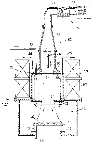
The construction of a typical e~ample o~ the
above-mentioned plasma processing apparatuses i5 shown in
Fig. 2.
In Fig~ 2, reference numeral 10 denotes a specirnen
chamber; 20, a plasma formation chamber; and 30, a microwave
suppl~ means.
The specimen chamber 10 has a specimen table 11 for
supporting a specimen (wafer, for instance) ~0 and is
communicated through gas holes 12 with an e~haust passage 13.
The plasma formation chamber 20 is communicated with
the specimen chamber 10 through a plasma extracting orifice
21 on the opposite side of the gas holes 12 and a first gas
is introduced into the chamber 20 through a first gas
introduction system or pipe 22 from a first gas source
outside of the chamber 20. An annular pipe 23 having a
plurality of small holes is disposed in the vicinity of the
outside portion of the orifice 21, so that a second gas is
introduced from a second gas source through a second gas
introduction system or pipe 24 into the specimen chamber 10.
A cooling ring portion 25 surrounds the chamber 20 and a
coolant such as water is supplied to the cooling ring portion
25 through a cooling pipe 26 from a coolant source.
A microwave introducing window 27, which is, for
instance, made of a silica glass plate is disposed on the end
wall of the plasma formation chamber 20 on the opposite side
of the orifice 21. The microwave from the microwave supply
means 30 is introduced into the plasma formation chamber 20
through the window 27, so that the first gas introduced into
the chamber 20 through the gas introduction pipe 22 is formed
into the plasma.
The microwave supply means 30 comprises a microwave
source 31 such as a magnetron which generates rnicrowave
having a frequency of, for instance, 2.~5GHz, rectangular
waveguides 32 and 33 for propagating the microwave from the
microwave source 31 toward the window 27 and a matching tuner
34 interposed between the waveguides 32 and 33. In this
case, the microwave is propagated in the TE mode into the
- 14 -
.
~9~773
plasma formation chamber 20 through the microwave
introduction window 27. Thus, the microwave propa~ated
through the introducing window 27 from the rectangular
waveguide 33 excites the first gas introduced into the plasma
formation chamber 20 to form the plasmaO
Electromagnetic coils 50 are disposed to surround the
plasma formation chamber 20 in such a way that the plasma of
the first gas formed by the electron cyclotron resonance of
the introduced microwave is introduced into the specimen
chamber 10 through the plasma extracting orifice 21.
The conventional plasma processing apparatus has in
general the construction just described above.
In the case of the plasma processing apparatus of the
type described above, the specimens 40 which are mounted on
the specimen table 11 are effectively processed by the plasma
thus produced, so that the plasma etching or deposition can
be accomplished.
The plasma processing apparatus of the type utilizing
plasma formed by the electron cyclotron resonance (ECR) has a
variety of features. When they are applied to CVD, various
thin films such as SiO2, Si3N4 and so on which have a high
degree of density and also a high quality can be manufactured
at a low temperature without heating and furthermore the
damages to the substrate can be minimized. In the
application to an etching process, the plasma processing
apparatus has features of a high accuracy, a high selection
ratio and minimum damage, so that the apparatus is essential
in the case of the future fabrication of vLSI circuit.
In the case of the above-described conventional plasma
processing apparatus, however, the microwave which excites
the gas introduced into the plasma formation chamber 20 is in
the TE mode so that the reflection of the microwave from the
plasma formation chamber 20 is high, so that the plasma
formation becomes unstable and therefore there was the
problem that the first gas cannot be excited effectively.
- 15 -
~2~77~
In addition, the conventional plasma processing
apparatus is in general so designed and constructed based
upon the processing by each specimen. Therefore, the
throughput characteristics such as a processing rate and so
on are not sufficient and accordingly there has been a great
demand for improving these characteristics. In other words,
it is required that an intensity of plasma and an ion current
density be increased without deteriorating other advantages.
FIRST EMBODIMENT: (Plasma Proc0ssing Apparatus)
A first embodiment of the present invention is shown
in Figs. 1 and 3, in which same reference numerals as those
used in Fig. 2 are also used to desiqnate the corresponding
portions and their details will not be explained here.
In Figs. 1 and 3, reference numeral 60 denotes a
microwave introduction unit comprising a circular waveguide
61 coupled to the microwave introducing window 27, a tapered
waveguide which is tapered from a rectangular shape to a
circular shape in order to transform the TE wave in the TElo
mode in the rectangular waveguide 33 into the TE wave in the
TEll mode in the circular waveguide 61 and a dielectric
member 63, for example, a silica glass plate which is
disposed inside the circular waveguide 61. This plate 63 is
disposed in parallel with the direction of the propagation of
the microwave introduced into the waveguide 61 and is also
perpendicular to the electric field of the microwave. The
window 27 is mounted to the plasma formation chamber 20 by a
supporting member 68. The circular waveguide 61 is fi~ed to
the supporting member 68.
The microwave which has been propagating in the
rectangular waveguide 33 is the TE wave (generally in the
TElo mode) whose electric field E is perpendicular to the
propagation direction Z. The TE wave is transformed into
7~3
the TE wave in the TEll mode by the tapered waveguide 62
and is introduced into the circular waveguide 61. A
portion of the TE wave introduced into the circular
waveguide 61 is transformed into the TM wave in a mode in
which the electric field of the microwave has a
longitudinal wave component by the dielectric plate 63 and
the IM wave is propagated through the circular waveguide 61
toward the microwave introducing window 27.
Fig. 4 shows an electric field distribution of
the microwave which is produced around the microwave
waveguide by the dielectric plate 63. ~his microwave is
the ~M wave having electric field components in the same
direction as the microwave propagation direction Z.
Therefore, the microwave introduced into the
plasma formation chamber 20 through the microwave
introduing window 27 is the microwave in the hybrid mode,
in which the microwave in the TM mode and the microwave in
the TEll mode, into which the microwave from the waveguide
33 is transformed by the tapered waveguide 62 and which is
introduced into the circular waveguide 61, c oe xist. This
microwave in the hybrid mode is called HE mode or EH mode
microwave, depending upon whether its major mode thereof is
the TE mode or TM mode. In the present invention, the
microwave in either HE mode or ~I mode can be used. In
other words, in the present invention, it is sufficient
that an electric field having a component in the direction
of the propagation of the microwave is introduced into the
plasma confined in the plasma formation chamber 20.
~3
Then, the electrons in the plasrka in spiral
mo t ion du e to th e e 1 ec tr on i c cyc lo tr on move men t a r ou nd th e
magnetic field in the Z-direction generated by the
electromagnetic coils S0 can satisfactorily interact with
S the electric field having a component in t:he Z-direction,
so that the stable mode is maintained and therefore the
microwave can efficiently propagate to the electron
cyclotron resonance region. As a result, the introduced
microwave is efficiency absorbed by the plasma, so that the
10 microwave reflected by the plasma is remarkably decreased.
Ihe reason why the electrons in spiral motion
easily interact with the electric field having a component
in the Z-direction is that the tion of the electrons in
the direction perpend icular to the Z-d irection is
lS decelerated due to the restricting force by the magnetic
field in the Z-direction, but the movement of the electrons
in the same direction as the direction of the magnetic
field is free without being restr icted by the magnetic
field .
SECOND EMBODIMENT: (Plasma Processing Apparatus)
Figs. 5, h~, 6B and 7 show a second embodiment of
the present invetion.
In the second embod iment, the circular waveguide
25 61 in the first embod iment is eliminated and a dielectric
plate 63 is disposed in the tapered waveguide 62 for mode
transformation in such a way that the plate 63 is
hor izontal in the Z-direction of the propagation of the
microwave and perpendicular to the electric field E of the
-- 1~ --
~3
microwave. In other words, in the second embodiment, the
tapered waveguide 62 and the mode transforming portion
consis~ing of the circular waveguide 61 and the dielectric
plate 63 are integrally structured. In this marlner, the
mode transformer for introducing the microwave can be made
compact in size.
Further, reference numerals 65 and 66 denote
lower and upper flanges of the tapered waveguide 62. The
lower flange 65 is secured to the supporting member 68.
According to the second embodiment, the tapered
waveguide 62 is so designed and constructed that the
rectangular section of the rectangular waveguide 33 is
transformed into a circular section having a diameter
substantially equal to the longitudinal length of the
rectangular section (for instance, lOcm~). The outer
appearance of the tapered pipe 62 is shown in Fig. 7.
Furthermore, the dielectric plate 63 disposed in the
tapered waveguide 62 is made of a silica glass plate
having, for instance, a length of 8cm in the direction of
the mic.owave propagation, a width of lOcm in the direction
perpendicular to the propagation direction and a thickness
of 5mm. The microwave introducing window 27 serves to
maintain the plasma formation chamber 20 in a vacuum
condition (a low gas pressure) and also to introduce the
microwave into the plasma formation chamber 20. In the
second embodiment, a silica glass plate having a thickness
of 15mm is used.
As shown in Fig. 8, the microwave which has
propagated through the rectangular waveguide 33 in the TElo
.
. ~ ,
~l29~773
mode is partly transformed into the lM mode wave (the
surface wave on the dielec ~ ic plate) in the tapered
waveguide 62 in which the dielectric plate 63 ~serves as a
transmission line. As a consequence, the TE wave and the
T~ wave coe~ist, so that the microwave in the hybrid mode
whose electric field has a longitudinal wave component is
introduced into the plasma formation chamber 20 ~ rough the
microwave introducing window 27 and then is combined with
and absorbed by the plasma in the chamber 20~
As mentioned above, the plasma, which is confined
within a limited space which is substantially equal in size
to the wavelength of microwave (or smaller than the
wavelength), permits the propagation of electromagnetic
wave having a longitudinal wave component. Thus, it is
considered that the waveguide mode having an electric field
component in the direction of the propa~ation of the
microwave facilitates the introduction of the microwave
into the plasma.
FurthermDre, because the microwave propagates
along the dielectric plate 63, the microwave is hardly
adversely affected by the shape of the circular waveguide
61 or the metal wall of the tapered waveguide 62
surrounding the plate 63. Therefore, the complicated
instability such as the reflection of the microwave due to
the surface unevenness of the metal wall and so on can be
eliminated.
,~,
..~,
- ~n -
73
EXPERIMENTS:
An oxygen (0~) ga5 was introduced into the plasma
formation chamber 20 from the gas introducing pipe 22 at a
flow rate of 5-50cc/min, 50 that the gas pressure in the
plasma formation chamber 20 was maintained at 10-4 Torr
-2xl~3Torr. A current within a wide range between 14 and
22A was supplied to the magnetic coils 50, so that the
conditions for generating the electronic cyclotron
resonance were established in some region in the plasma
formation chamber 20. By adjusting the tuner 34, the
following satisfactory results were obtained.
Furthermore, the ionization rate of the plasma
was increased by about three times with the same microwave
power introduced. Moreover, the reflection of the
microwRve was largely reduced, so that it became possible
that the microwave having a power higher than the
conventionally used microwave is introduced into the plasma
formation chamber 20. As compared with the conventional
apparatus, an ion current (10-20mA/cm2~ m~re than ten times
as high as the conventional ion current was extracted into
the specimen chamber 10 in which the specimens 40 were
disposed.
When a pulse-shaped (intermittent oscillation)
microwave (intermittent oscillation of 5OHz and lOOHz at a
frequency of 2.45GHz), which adversely affects the matching
of the microwaves, was used, the reflected wave of 40-50~
of the microwave was observed when the microwave power of
200-lOOOW was supplied to the conventional apparatus, but
in the case of the apparatus in accordance with the pre æ nt
37~
invention, only 2-8% of the microwave was reflected. Thus,
the character istics of the plasma processing apparatus are
considerably improved in accordance with the present
i nvent ion .
So far it has been described that the dielectric
Tember 63 is in the form of plate, but it is apparent that
a dielectric member in the form of cylinder may be equally
used as the dielectric member 63. In the latter case, a
mode of the propagation of the microwave is mainly the HE
mode.
Figs. 9A and 9B show a specific embodiment of the
tapered waveguide 62. E~re, reference numeral 67
designates a plurality of holes 67 opened in the lower
f lange 65 . Ihe lower f lang e 65 is secu red to the
L5 supporting member 68 of the window 27 by inærting bolts
into holes 67. Reference numeral 69 denotes a plurality of
holes opened in the upper flange 66. The upper flange 66
is secured to the rectangular waveguide 33 by inserting
bolts into the holes 69. Reference numerals 70 and 71, and
reference numerals 72 and 73 designate two pairs of two
elongated pro jection members which are mounted to the inner
wall of the tapered waveguide 62 and the members 70 and 71,
and 72 and 73 are spaced apart from each other by a
predetermined distance, respectively. The pair of the
projection members 70 and 71 are opposed to the other pair
of the pro ject ion member s 72 and 73. Grooves de fined by
the pair of the projection members 70 and 71 and the yair
of the pro jection members 72 and 73 serve to guide the both
opposite ends of the s ilica glass plate 63. The lower end
-- 2 2 --
~l29~73
of the silica glass plate 63 may be made into contact with
the window 27. Alternatively, the lower erx~s o~ the
pro jection members 7 ~ 73 may have a member for supporting
the silica glass plate 63. Further, reference numeral 74
5 represents a lower circular opening and reference numeral
75 denotes an upper rectangular opening.
In this embodiment, the tapered waveguide 62 was
made of copper and the surfaces thereof were plated with
silver. The upper rectangular opening 74 was about 30x90mm
10 and the lower circular opening 74 was lOOmm in diameter.
The tapered waveguide 62 was llOmm in height. Ihe silica
glass plate 63 was 99x80mm and 5mm in thickness. The cross
section of each of the pro jection members 7t) 73 was 2~2mm
and each projection member was lOOmm in length. The
15 spacing between the pro jection members 7 0 and 71 and the
spacing between the pro jection members 72 and 73 were 6mm~
The respective lower ends of the pro jection members 7~73
were spaced apart by Smm from the lower circular opening
74, and the respective upper ends of the projection members
20 7~73 were spaced apart by 5mm from the upper rectar,gular
opening 75.
T~IRD EMBODIMENT: (Plasma Process ing Apparatus)
The third embodiment of the present invention
25 shown in Fig. 10 is a modification of the second embodiment
shown in Fig. 5 . In th is th ird embod imen t, in order to
further improve the matching characteristic, another
dielectric plate which is, for instance, a PTFE plate of 5-
lOmm in th ickness is superposed on the microwave
30 introducing window 27.
-- 23 --
7~3
Furthermore, the matching characteristics of
various ECR plasma processing apparatus were optimized by
changing the len~th (5-lOcm in the experiments) of the
dielctric plate 63 inserted into the mode transforming
portion.
Referring next to Figs. 11, 12 and 13,
explanation will be made of propagation characteristic of
the microwave in the plasma to which the magnetic field
generated by the electromagnetic coils 50 is applied. The
dispersion relationships in the respective modes of the
microwave propagating through the plasma, that is, the
relationships between the frequency ~ and the wave number k
are expressed approximately as shown below:
In the case of the HE wave:
aTJn' (aT) (~2~1~o-k2)
+n~2~2~oJn(aT)=o
, where Jn(x): Bessel function
and
T 2 = ( ~ o~ 2-k2.
In the case of the EH wave:
Jn(aT) = 0
and
T2= ~3 (~1~o~2-k2)-
Figs. 11 and 12 show the dispersion relationshipsof the HE wave and the EH wave in accordance with the
present invention. Here, both the HE wave and the EH wave
-~4-
are hybrid waves and can be referred to as a quasi-TE wave
and a quasi-TM wave, respectively.
The frequency ~/WC obtained by the normalization
oE the microwave frequency ~ by the e.lectron cyclotron
frequency ~c=eB/m is plotted alon~ the ordinate, while the
wave number k/kc obtained by the normalization of the wave
number k by kc=~c/c ~where c is the light speed) is plotted
along the abscissa.
In the case of the HE wave shown in Fig. 11,
~c/2~ was determined to be 3GHz and a plasma radius was
determined to be lOcm, under the conditions that a high
density plasma of ~p/wc=1.5 was generated with respect to
the plasma frequency ~p=~ne2/~Om . In Fig. 11, wh is the
hybrid resonance frequency and is given byl~c2+~p2 .
In the case of the EH wave shown in Fig. 12, the
same calculation conditions are used. The E~ll mode
extending from the original point can be utilized to
improve the plasma generation efficiency~ The high density
plasma condition ~p/~c>l was obtained when ~c/2~=2.45GHz
and the plasma density ~ was n>7.45xlOlOcm~3.
Fig. 13 shows the distribution of a magnetic flux
density B of the magnetic field in the Z-direction in the
plasma formation chamber 20 in the apparatus in accordance
with the present invention. When ~/2~=2.45GHz, the
electron cyclotron resonance (ECR) occurs at B=875G and
~=~c is satisfied.
As is easily understood from Figs. 11 and 12, at
a microwave frequency where k ~ ~, the microwave resonates
with the electrons in the plasma, so that the electron
- 25 -
~9~773
cyclotron resonance is conditioned. The HE wave resonates
at the frequencies cf ~c and w~l, while the ~l ~ave
resonates at the frequencies of ~c and ~ Ln the case of
the EH wave, there is no difference betwe~n the right-
handed wave (n=l) and the left-handed wave (n=-l) of the
rotation of the electric field with respec~ to the
propagation direction of the microwave and in the case of
the HE wave, the difference is very small.
The HE wave mode and the EH wave mode extending
from a point adjacent to the origin are the modes in which
the microwave is propagable under the condition that both
the plasma and the static magnetic field exist. These
modes disappear when ~p ~ 0 (the condition that no plasma
is generated) and become the waveguide modes of the
conventional TE and TM wave.
In the case of the HE wave, the electric field is
strong in the periphery of the waveguide. But, the EH wave
has a strong electric field even in the central portion, so
that the plasma can be effectively formed. The EH wave
resonates at ~p under the condition that the density of the
plasma is low (~p<~c) But~ the EH wave resonates at ~c
under the condition that the density of the plasma is high
(~p>~c) The frequency ~c is determined only by the
intensity of the magnetic field, so that it is stable.
Accordingly, in order to increase the intensity
of the ECR plasma in a stable excitation state, the EH wave
mode (quasi-TM wave) extending from the original point is
effective.
- 26 -
77;~
From the results of the above-describ~d theore-tical
analysis, it is considered that it is effective to utilize a
mode e~tending from a point adjacent to the origin point in
the hybrid wa~e (the EH wave~ having an electric field
component even in the propagation direction of the microwave,
as the propagation mode for introducing the microwave from
the strong maynetic field (~ c>~ ) to the region in which the
ECR conditions are satisfied. On the other hand, the
microwave which propagates through the rectangular waveguide
is the TE wave whose electric field is perpendicular to the
propagation direction of the microwave, so that it is not
suitable for e~citing the hybrid wave (EH wave).
In view of the above, according to one aspect of the
present invention, the TE wave from the rectangular waveguide
33 is introduced into the mode transformer including the
dielectric member 63 to induce the TM wave, which is in the
dielectric wave mode, whereby the TE and TM waves coexist and
the hybrid wave in the propagation mode having the
longitudinal wave component is extracted and introduced into
the plasma formation chamber 20. As a result, the microwave
is easily transformed into the propagation mode in the
plasma, so that the energy of the microwave can be
efficiently supplied to the plasma region in which the ECR
conditions are satisfied and is absorbed. Thus, the plasma
formation efficiency is considerably improved.
- 27 -
~2~ 3
FOURTH EMBODIMENT: (ECR Etching Apparatus)
The plasma processing apparatus shown in Fig. 5
is applied to the ECR etching appara hls disclosed, for
example, J. Vac. Sci. Technol B4(3) 696 (1986).
S ~.ore specifically, in the E~R plasma processing
apparatus constructed as shown in Fig. 5, an etching gas is
introduced into the plasma formation chamber 20 from the
gas introduction pipe 22, so that the apparatus can be used
as an etching apparatus. In this case, the inner wall of
the plamsa formation chamber 20 is lined by silica glass so
that the inner wall (metal) of the plasma formation chamber
20 is not etched by the etehing gas or the specimen (wafer)
40 to be etched is not contaminated by the metal of the
inner wall. While in this embodimRnt the etching gas was
supplied from the first gas introduction system 22, both
the first and seeond gas introduction systems 22 and 24 can
be used.
In the ECR etching apparatus thus constructed,
the microwave introducing unit 60 in accordance with the
present invention is interposed between the rectangular
waveguide 33 and the microwave introducing window 27 so
that a part of the TE wave from the reetangular waveguide
33 is transformed into the TM wave by the mode transformer
including the dielectric member 63, so that hybrid wave
containing a longitudinal wave component is introduced into
the plasma formation chamber 20 through the microwave
introducing window 27.
In the ECR etching apparatus thus constructed, an
etching gas consisting of C12 75 volume ~ an~ SF6 2S
-- 28 ~
1~G~ ~773
volume % at the flow rate of 20sccm was supplied through the
gas introduction pipe 22 to the plasma Eormation chamber 20.
In this case, the relationship between the microwave power
and the ion current density; that is, the ion extraction
characteristics and the reflected microwave power; that is,
the microwave reflection characteristics are shown in
Fig. 14, where the present invention is compared with the
prior art. Further, the reflected wave was measured under
the condition that the reflectPd wave was minimized by
adjusting the tuner 34.
As is apparent from Fig. 14, according to an aspect of
the present invention, the ion current density was increased
by three-four times in response to the introduced power
substantially equal to that used in the conventional
apparatus. Therefore, a high ion current density of lOmA/cm2
or more was uniformly obtained in the region having a
diameter of 15cm or more. Furthermore, the r~flected wave
was lOw or less, so that the reflected wave was negligible.
Therefore, when the introduced microwave power is further
increased, the ion current can be further increased. In this
embodiment, in order to elirninate the current due to the
incident electrons, the measurement of the ion current
density was made by a probe biased to a negative voltaye of
-SOV. As the microwave source 31, use was made of a
continuous oscillation type at the frequency of 20~5GHz, but
it is also possible to use other frequencies or the
intermittent oscillation type microwave source.
- 29 -
~29~77;~
Fig. 15 illustrates characterstics of an etch
rate for silicon etching when a mixing ratio between C12
and SF6 which constitute an etching gas.
When C12 is ~e major component, the etching
process is promoted by the ion incidence, so that the
etching process can be accomplished at a high degree of
accuracy without undercuts. According to the pre æ nt
invention, in this region, the etch rate can be remarkably
increased and especially under the condition that SF6 is
25~ or less, the etch rate is remarkably increased by about
ten times. In this embodiment, the ECR plasma is extracted
by the divergent magnetic field to produce an ion stream.
Consequently, the ion energy is low a ~ is of the order of
10-30eV. Thus, there are advantages in that damages to the
silicon specimens can be minimized in that the
characteristics of the selective etching with respect to a
primary layer material is satisfactoryO In the caæ of a
low energy, the prior art method has a disadvantage that
the etch rate is low, but according to the present
invention, a sufficiently high etch rate can oe attained.
Furthermore, when a bias voltage is additionally
applied to the specimen table by a high frequency electric
power source in combination with this embodiment, the etch
rate can be further increased by a few time. However, in
this caæ , the advantage of the low energy is lost, so that
it is advisable to distinguish between the uses of the two
manners in accordance with a purpose.
As is apparent from Fig. 14, the etch rate is
increased by increasing the flow rate of an etching gas
,~.. .. .
- 30 -
~.~9~7~
and/or the microwave power, so that the throughput can be
fu r the r i nc rea se d .
Further, it has been confirmed that the
character istics such as an etching ~election ratio, damages
5 to the specimen and so on which are advantageously obtained
in the prior art apparatus are not lost.
Fig. 16 illustrates an example of the etching
cha rac ter ist ics ob ta in ed by the p re sen t i nven t ion . In th is
case, a mixed gas consisting of C12 and SF6 was used as an
10 etching gas, whose flow rate was 20 sccm (at the pressure
of 5.0x1~4 Torr) and the microwave power was 400W Fig.
16 illustrates etch rates in the caæs of a single crystal
si licon and poly si licon and etching ælection ratios in
the cases of Poly-Si/SiO2 and Poly-Si/resist (OFPR or AZ).
As is apparent from Fig. 16, the characteristic
of a hi~h selection ratio (Poly-Si/SiO2 is 50 or more) on
the side of C12 (C12 only or containing SF6 slightly) which
is a feature of the low energy ion stream etching process
is not lost at all, as con~ared with the prior art l~R
Z0 me thod .
As to the evaluation of the crystal deects of Si
after the Si etching prccess, the evaluation results in
that this method causes extremely small damage as compared
with the convention high frequency plasma processO
These results show that the ion current density
can be increased by the application of the present
invention, wh ile the ion energy is hardly increased, 50
that the improvement o~ the throughput does not adver se ly
a ffec t oth er charac te r is~ ic s.
.
: -.
31 -
773
FIF~I EM~ODIMENT: (ECR Plasma CVD Apparatus~
The ECR thin film forming apparatus disclosed in
U.S. Patent Nb. 4,401,054 entitled as "Plasma ~position
Apparatus: or U.S. Patent No. 4,492,620 entitled as "P ~sma
Deposition Method and Apparatus" is used and tbe microwave
introduction unit 60 in accordance with the present
invention is disposed at the microwave introduction unit of
the above-mentioned apparatus so that a part of the TE wave
from the rectangular waveguide 33 is transformed into the
TM wave by the m~de transformer including the dielectric
member 63. The hybrid wave containing a longitudinal wave
component is introduced into the plasma formation chamber
20 through the microwave introducing window 27.
Microwave reflection characteristics, i.e.,
matching characteristics obtained when a current to be
supplied to the electromagnetic coils 50 is varied in the
ECR plasma CVD apparatus thus constructed are shown in Fig.
17, with comparing the present invention and the prior art.
The power of the incident microwave was 300W and
an 2 gas was introduced into the plasma for~ation chamber
20 through the gas introduction pipe 22 at the flow rate of
30cc/min or 5cc/min. The reflected microwave was measured
under a condition that the power of the reflected microwave
is minimized by adjusting the tuner 34.
In Fig. 17, ~hen the current supplied to the
electromagnetic coils 50 is increased to about 1~ , a
magnetic flux density of the magnetic field which satisfies
the ECR conditions (875G in the case of the frequency
2.45GHz of the microwave) appears in one portion within the
- 32
77;~
plasma formation chamber 20 r so that the p]asma is
generated. When the current thro~h the eLectromagnetic
coils S0 is further increased, the magnetic field reg ion
which satisfies the E~R conditions is d isplaced toward the
5 center portion of the plasma formation chamber 20 from the
vicinity of the microwave introducing window 27. When the
electromagnetic coil current is in the rar~e between 16 and
20A satisfying the E~R conditions, the reflected microwave
bec ame 1 ~6 or le ss trh en th e f lo w r a te o f th e O 2 g as wa s
10 30cc/min. Even at the flow rate of 5cc/min, the reflected
microwave became ~6% or less. Thus, as compared with the
prior art, it was recognized that the matching
character istic was remarkably increased.
Fig. 18 illustrates the variations in the
15 reflectivity when the power of the incident microwave was
var ied, in ca se that the f low rate of the 2 gas was
30cc/min and the current flowing through the
electromagnetic coi ls 50 was 1&~ .
As is apparent from Fig. 18, even if the power of
20 the microwave is varied over a wide range, the reflectivity
is limited within a low value of 1-2~6, so that it is found
ou t th a t th e ma tc h ing c h arac te r is t ic is i mp rov ed .
Further, in the above-mentioned apparatus, an
intermittent type oscillator was used as the microwave
25 source 31. Thus, even though an instantaneous value of the
power; that is, the plasma condition varies from time to
t ime, th e sa t is fac to ry ma tc h ing c harac te r ist ic wa s a tta in ed
as illustrated in Fig. 18.
. - - 33
~2~7'73
When both the 2 gas and the SiH~ gas were
introduced into the above-mentioned CVD apparatus to
deposite an SiO2 Eilm, the relationship between the
microwave power and the deposition rate and the microwave
power and the reflectivity were obtained as illustrated in
Fig. 19.
This characteristic shows the results measured
when the current flowing through the electromagnet coils 50
was 17A; the distance between the specimens 40 on the
specimen table 11 was 15cm; and the gas introduction
conditions were so determined that the flow rate of the 2
gas was 30cc/min and 50cc~min and the flow rate of the SiH4
gas was 30cc/min and 50cc/min (in terms of N2). When
SiH4:02=50:50cc/min, and the power of the microwave was
1200W, the deposition rate was 4000A/min, and consequently
the film was formed at a rate two or three times as high as
the deposition rate obtained by the prior art apparatus.
Therefore, the throughput of the fiLm formation was
increased. In this case, even when the power of the
microwave was increased, the refractive index was
maintained substantially at about 1.48~ and thus the
quality of the grown film was high. Even if the power of
the microwave was further increased, the reflectivity was
maintained at about 1~ or less, so that it is understood
that the reflective power was reduced to a negligible
level.
So far, even when a high power of the microwave
is supplied, the reflected power is increased, so that it
is difficult to increase the power of the microwave
- 34
37'73
injected into the plasma. In contrast, according to one
aspect of the present invention, it becomes easy to inject a
high power microwave into the plasma. As a result, the
deposition rate can be further in~reased to a high rate ~for
instance, 1~ m/min) which is two or three times as high as
the deposition rate attained by the prior art apparatus by
increasing the flow rate of the deposition gas.
As is clear from the above, according to one aspect of
the present invention, the microwave in the TE rnode from the
rectangular waveguide is supplied to the mode transformer and
is partially transformed into the TM wave by the mode
trans~ormer, so that the hybrid wave in the propagation mode
having an electric field component parallel to the direction
of the microwave propagation; that is, a longitudinal wave
component is introduced into the plasma formation chamber.
As a result, the microwave energy is efficiently supplied to
the plasma region which satisfies the ECR conditions and then
is absorbed by the plasma, so that the efficiency of the
plasma formation is enhanced and accordingly the throughput
of the plasma processing is improved.
F~rthermore, according to one aspect of the present
invention, the power of the microwave which is reflected back
without being introduced into the plasma formation chamber is
considerably decreased, so that the microwave is efficiently
injected into the plasma. Moreover, according to one aspect
of the present invention, there is an advantage in that the
reflectivity is maintained at a low value, even if the power
of the microwave is varied over a wide range.
Therefore, according to one aspect of the present
invention, the microwave supply source can be made larger in
capacity and in addition the flow rate of the gas to be
introduced is increased, so that the throughput of the plasma
processing can be further improved.
As a result, one aspect of the present invention can
be equally applied to ECR plasma etching apparatuses and an
ECR plasma CVD apparatus, so that the etch rate and the film
deposition rate can be improved, respectively. Furthermore,
- 35 -
~8~ 3
one aspect of the present invention may be equally applied
not only to the above-mentioned apparatuses, but also to
other various apparatuses utilizing the microwave plasma such
as an ion shower apparatus (for e~ample, the apparatus
disclosed in U.S. Patent No. 4,450,031), an ion beam
apparatus, an ECR plasma sputterin~ apparatus and so on, so
that their characteristics such as the ion current can be
improved.
The invention has been described in detail with
respect to various embodiments, and it will now be apparent
from the foregoing to those skilled in the art that changes
and modifications may be made without departing from the
invention in its broader aspects.
- 36 -
~. .