Note: Descriptions are shown in the official language in which they were submitted.
306~L
DETERMINATlON OF ELECTRICAL CAPACITANC~ AND RESISTANCE
The invention relates to apparatus and methods for
determining capacitance and resistance values in an
electrical component. An apparatus and method
according to the invention may be used for determining
capacitance and resistance values of an electrical
sensor, such as a fuel level sensor, having both
capacitive and resistive characteristics.
Various sensor applications use the change in
capacitance of a sensor as an indication of a physical
parameter to be measured. For example, in measuring
the level of fuel in a fuel tank, a capacitive probe is
positioned within the tank. The probe typically
includes structure which defines capacitor plates or
the functional equivalent with the dielectric constant
between the plates determined by the level of the fuel
in the tank as well as the air in the airspace above
the fuel. The sensed capacitance is a function, in
part, of the fuel level in the tank. ln an optimal
capacitive-type sensing system, the electrical
resistance between the plates is very high, of the
order of hundreds of megohms and normally does not
influence the capacitive sensing function. However,
under certain circumstances, abnormal conditions within
~3011~6~4
the fuel tank can contribute to an unusu~lly 19w
resistance path between the capacitive plates, A low
resi~tance condition can adversely affect the validity of
the capacitance measurement. 5uch abnormal conditions
include, for esample, the presence of water in the fuel
tank, contaminants that possess electrolytic properties,
and microorganisms in the fuel. Thus, in sensing fuel
levels using capacitive probes, it is also important to
sense resistance between the pla~es of the probe to
determine the ~eneral conditions within the tank and
provide an indication of those conditions which may
adversely affect capacitance measurements.
According to the invention, there is provided an apparatus
~or determining capacitance and resistance characteristics
of an electrical Aevice, comprising means for subjecting
an electrical component to a vol~age signal having a
linear ramp portion which passes from a first polarity
through zero to a second polarity h~ving ~ fised voltage
level, means for sensing the voltage potential across the
electrical component in response to the ~ero crossing of
the voltage signal and for seDsing the voltage potential
across the alectrical componcnt when ~he voltaqe is at the
fized voltage level, and means for determinin~ the
capacitance of the ~lectrical component from the voltage
potential sensed in r~sponse to the zero crossing and for
.~
~3006~34
determining the resistance of the electrical component
from the voltage potential sensed at the fised voltage
level.
According to the invention, there is also provided a
sy~Sem for determinin~ capacitance and resistance
characteristics of a capacitive fuel level sensing probe,
comprising means fcr subjecting a capacitive fuel level
sensing probe to a voltage signal including a linear ramp
voltagP that passes from a first pol~rity throu~h zero to
a second polari~y havin~ a fixed voltage level, means for
sensing the volta~e potential across the sensing probe in
response to th~ zero crossing of the time varying voltage
and or sensing the voltage potential acro~s the sensing
probe when the voltage is at the fised voltage level, and
means for determining the capacita~ce of the sensing probe
from the voltage potential sensed i~ response to the zero
crossing and for determining the resistance o the sensing
probe ~rom the voltage potential sensed at the fi~ed
voltage level.
According to the invention, there is ~ur~her provided a
method of determining ~apacitive an~ resistive
characteristics of an electrical component, comprising the
steps of subjecting an 21ectrical component to a v~ltage
signal including a linear ramp voltaqe that passes from a
~L3006~3~
first polarity through zero to a second pola~ity having a
fi~ed voltage level, sensing the voltage potential across
the electrical component in response to the zero crossing
and sensing the voltage potential across the component
when the voltage is at the ~lxed voltage level, and
determining the capacitance of the electrical component
from the volta~e potential sensed in response to the zero
crossing and determining the resistance from the voltage
potential sensed at the fixed voltage level.
According to the invention, there is still further a
method of determining capacitive and resistive
characteristics o~ a capacitive ~uel level sensing probe,
comprising the steps o subjectiny a capacitive fuel level
sensing probe to a ~oltage signal including a linear ramp
voltage that passes from ~ first polarity through zero to
a second polarity having a fi~e~ voltage level, sensing
the voltage potential across the electrical component in
response to the zero crossing and sensing the voltage
potential across the electrical component when the voltage
is at the ~ixed vol~age level, ~nd d~tsrmining the
capacitance of the electrical component from the voltage
potential sensed in response to the z~ro crossing and
determining the resistance of the electrical component
from the volt2ge potential sensed at the fi~ed voltage
level, subjecting a calibration standard having known
, .
.
.
13() [)684
capacitive and resistive characteristics to a time rarying
voltage including a linear ramp voltage tha~ p~sses from a
first polarity through zero to a second polarity having a
fixed voltage level, sensing the voltage potential across
the calibration standard in response to the zero crossing
and sensing the voltage potential across ~he c~libra~ion
standard when the v~ltage is at the fixed voltage level,
determining the difference in capacitance and resistance
of the sensing probe and the calibration standard
electrical component from the vol~age potential sensed in
respons2 to the respective zero crossings and the voltage
potentials sensed at the fised voltage levels, and
correcting the capacitance and resistance values of the
sensing probe as a function of the measured capacitance
and ~esistance values of the calibration standard.
Apparatus embodying the invention and methods accordinq to
the invention, for determining capacitance and resistance
values of an electrical component, such as a liquid level
sensor, will now be described, by way of e~ample only,
with reference to the accompanying drawings in which:-
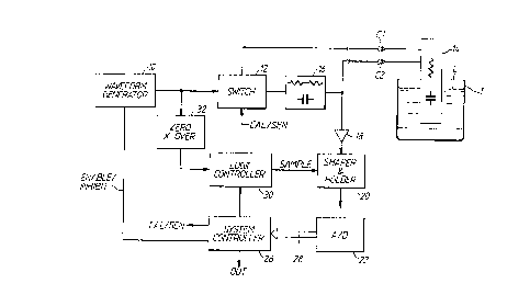
Fig. 1 is a schematic block diagram of a circuit of theapparatus; and
Fig. 2 is an idealized grap~ical illustration of an
~'
~3(~06~4
interrogation waveform used in the circuit of Fig. 1.
As shown in schematic form in Fig. 1, a waveform
generator 10 is connected to a switch 12 which, in
turn, provides a switched output to either a sensor
unit 14 or a calibration standard 16. as shown, the
sensor unit 14 is connected in circuit through a
connection interface Cl/C2, and if desired, can be
located in a remote position from the schematic circuit
of Fig. 1. In the preferred embodiment, the sensor
unit 14 is a capacitive probe mounted in a tank T
containing a selected quantity of a liquid L, such as
fuel. The sensor unit 14 and the calibration standard
16 are connected to a preamplifier 18 which provides an
amplified output to a sample and hold circuit 20 which
functions, as described more fully below, to sense
representative voltage potentials from the sensor unit
14 or the calibration standard 16 in response to an
appropriate command. The analog output of the sample
and hold circuit 20 is provided to an analog-to-digial
converter 22 which converts the analog value provided
by the sample and hold circuit 20 to a corresponding
multi-bit binary value. A system controller 26 accepts
the digital values provided via a bus 28 from the
analog-to-digital converter 22 and uses those values to
compute capacitance and resistance values and provide
~L3~06~
an appropriate output signal to an output port OUT.
The system controller 26 also provides control signals
to a logic controller 30 which periodically provides a
SAMPLE command to the sample and hold circuit 20 to
sense and retain the analog voltage values provided
through the preamplifier 18 by either the sensor unit
14 or the calibration standard 16. The system
controller 26 also provides appropriate ENABLE/INHIBIT
signals to the waveform generator 10 to initiate the
capacitance and resistance determination cycle as well
as a CAE/SEN signal to the switch 12 to select either
the sensor unit 14 for evaluation or the calibration
standard 16 to initiate an auto-calibration cycle. In
additionJ a zero cross-over detector 32 is connected to
the output of the waveform generator 10 and provides a
signal to the logic controller 30 indicating the moment
when the output of the waveform generator 10 passes
from a positive value through zero to a negative value
and, conversely, passes from a negative value through
zero to a positive value.
The waveform generator 10 provides a voltage output
having the profile shown in Fig. 2, that is, an initial
value of +V that decreases in a linear manner through
zero to a -V value and which then remains fixed at -V
for a selected period before rising in a linear manner
6~
from -V through zero and returning to the +V
potential. The output voltage profile shown in Fig. 2
is used to interrogate either the sensor unit 14 or the
calibration standard 16 and to determine the respective
capacitance and resistance values, as described below.
The switch 12 functions as the equivalent of a
single-pole, double-throw switch in response to the
CAL/SEN signal provided from the system controller 26.
When a CAL signal is provided, the switch 12 switches
the calibration standard 16 into the circuit to effect
auto-calibration and, when the SEN signal is provided,
the switch 12 switches the sensor unit 14 into the
circuit to determine the capacitance and resistance
values of the sensor unit 14. The preamplifier 18
preferably has a high input impedance and a gain
appropriate for the waveform repetition rate. The zero
cross-over detector 32 functions to detect the
cross-over of the linearly declining and rising
portions of the voltage profile of Fig. 2 and to
provide an appropriate output to the logic controller
30. While a number of devices can perform the zero
cross-over detect function, an operational amplifier
configured as a differential amplifier driving a
bi-stable device can provide the desired output signal
to the logic controller 30. The system controller 26
is preferably a stored-program controlled
~3~)06&19L
micro-processor including a ROM containing an
instruction set for implementing the functions
described below, a RAM for storing values presented by
the analog-to-digital converter 22, an accumulator, one
or more general purpose storage registers, and
input/output interfaces.
The circuit of Fig. 1 operates through an interrogation
cycle to determine the capacitance and resistance
values associated with the calibration standard 16 or
the sensor unit 14. Where the sensor unit 14 has been
selected by the system controller 26 and the
appropriate SEN signal presented to the switch 12, the
sensor unit 14 is placed in circuit with the waveform
generator 10 and the preamplifier 18 while the
calibration standard 16 is effectively disconnected.
In response to an ENABLE signal provided from the
system controller 26, the waveform generator 10
presents a time varying interrogation voltage through
the switch 12 to the sensor unit 14. The
interrogation voltage follows the profile shown in Fig.
2, starting at a +V value and declining in a linear
manner to the -V value. As the interrogation voltage
declines, the capacitance of the sensor unit 14 is
charged with the potential rising in a manner inverse
to the capacitance value. When the declining
~:~006~4
interrogation voltage intersects and passes through
zero, the zero cross-over detector 32 provides an
appropriate signal to the logic controller 30 which
commands the sample and hold circuit 20 to sample the
output of the preamplifier 18, which output is
representative of the capacitance-determined voltage
potential of the sensor unit 14. The sampled value is
converted to a digital value of selected bit width
(e.g., 16 bits) with the digital value presented to the
system controller 26 via the bus 28. The system
controller 26 then computes the capacitance value for
the sensor unit 14 and stores the computed value and/or
provides the computed value as an output signal OUT.
The capacitance determination can be accomplished by
algebraic computation or by table look-up where the
sensed voltage level is compared with empirically
determined voltages and corresponding capacitance
values.
In order to eEfect the resistance determination, the
system controller 26 presents an appropriate control
signal to the logic controller 30 so as again to cause
the sample and hold circuit 20 to sample the output of
the preamplifier 18. This second sample and hold
command occurs at a predetermined time period after the
detection of the zero crossing when the interrogation
` ;' '~,............. .
1 1
voltage is constant at the value -V prior to rising
linearly from -V to +V. The predetermined time period
is a function of the repetition rate of the waveEorm
generator 10. During the time period that the
interrogation voltage is fixed at the value -V, the
voltage potential sensed by the preamplifier 18 is
solely a function of the resistance of the sensor unit
14 and is independent of any capacitance effect. The
output of the sample and hold circuit 20 is provided to
the analog-to-digital converter 22 which, in a manner
analogous to that described above, provides a multi-bit
digital value to the system controller 26 to effect the
resistance determination.
In order to ensure the ultimate accuracy of the
capacitance and resistance measurements of the sensor
14, an auto~calibration function is performed using the
calibration standard 16. Measurement errors and other
inaccuracies can arise from a number of sources
including the time-varying voltages provided by the
waveform generator 10, hysteresis in the zero
cross-over detector 32, impedances in the switch 12,
and various other offsets and errors. In order to
perform an auto-calibration, the system controller 26
provides an appropriate CAL selection signal to the
switch 12 to switch the calibration standard 16 into
~L3~10684
the circuit and effectively disconnect the sensor unit
14. The waveform generator 10 is then enabled by an
appropriate command from the system controller 26 to
present the interrogation voltage through the switch 12
to the calibration standard 16. The sample and hold
circuit 20 then functions in the manner described above
to provide output values that are converted to digital
values and presented to the system controller 26 for
determination of the capacitance and resistance values
of the calibration standard 16. Since the capacitance
and resistance values of the calibration standard 16
are pre-determined, the difference between the
respective values determined by the system controller
26 and the pre-determined values represents a
calibration offset. Since the difference values for
the capacitance and resistance are in digital form, the
difference values are loaded into appropriate registers
or memory locations and used to oÇfset the measured
values for the sensor unit 14, which offset values can
be obtained immediately before or after a measurement
cycle using the sensor 14.
As can be appreciated from the above, the method and
apparatus described accurately determine capacitance
and resis~ance values for an electrical component
including various types of sensors. Additionally, an
~3~36~34
13
auto-calibration feature is provided whereby the
accuracy of the measurement is enhanced.
This it will be appreciated from the above that a
highly effective apparatus and method for determining
resistance and capacitance values is provided by which
the principal objective, among others, is complet~ly
fulfilled. It will be equally apparent and is
contemplated that modification and/or changes may be
made in the illustrated embodiment without departure
from the invention. Accordingly, it is expressly
intended that the foregoing description and
accompanying drawings are illustrative of preferred
embodiments only, not limiting, and that the true
spirit and scope of the present invention will be
determined by reference to the appended claims and
their legal equivalent.
0322S