Note: Descriptions are shown in the official language in which they were submitted.
~.3~}73~ 3~CA 84,323
WIDESC~EEN TELEVISION REOEPrION AND RECORDING
SYSTEM UTILIZING CO~VENTIONAL ~QUIPMENT
The present invention relates to apparatus for
converting a television signal which represents an image
having an aspect ratio such as 5:3 into a signal which may be
recorded by a conventional recorder and displayed either on a
10 conventional 4:3 aspect ratio receiver or on a widescreen
television receiver.
Recently, a great deal of interest has been expressed
;n television systems which provide an image aspect ratio
(i.e., the ratio of the width to the height of the image) such
as 2:1, 16:9 or 5:3, which is greater than the 4:3 aspect ratio
of television systems conforming to a conventional standard,
such as NTSC. The wider aspect ratios are more in-line with
human visual perception than the conventional 4:4 aspect
ratio. Consequently, present day motion picture films produce
2 () ;mages with an aspect ratio of 5:3 or greater.
lt is clesirable ~or a new transmission system, that
prodllces a wiclescreen television signal, to be compatible with the
existing transmission stan(l,lrcl and with existing conventiotlal
television receivers. This me,llls that the widescreen television
2 5 signal sholllcJ be cnp.lble of being transmitted through a single
channel of the convelltion.ll transmission system and that the
received widescreen signal be processed by a conventional
receiver so as to produce a conventional aspect ratio image,
without significant distortion.
3 0 One such compatible widescreen television
transmission system is described in U.S. Patent 4,816,899, entitled
"Compatible Widescreen Television System", of C. H. Strolle et al.
This system uses a widescreen television camera that is capable of
scanning a scene so as to generate a widescreen television
3 5 signal corresponding to an image having an aspect ratio
\
..
~3t:)~73~
-~- RCA 84,323
(e.g. 5:3) that is greater than the 4:3 aspect ratio of a
conventional television signal. The widescreen television
signal has an active line interval, containing one
horizontal line of image information, that is the same as
the active line interval of a conventional aspect ratio
television signal (e.g. approximately 52.5 microseconds for
NTSC).
If the image represented by a widescreen
television signal were reproduced directly on a
conventional television receiver, the image would appear to
be compressed in the horizontal direction; objects would
appear thinner than normal. Moreover, to achieve
equivalent horizontal resolution in the reproduced image,
the widescreen signal has a greater bandwidth than a
conventional signal. Conse~uently, there may also be a
loss in horizontal resolution if the widescreen signal is
transmitted through a conventional television channel.
To solve these problems, the widescreen
television system described in the Strolle et al. patent
application uses an ~ncoder to convert the widescreen
television signal into an encoded television signal which
co~ltains sufficient information to ~aithfully reproduce a
widescreen image and which is also compatible with the
conventional NTSC transmission system. When the encoded
signal is received and processed by a widescreen television
receiver, such as that described in the Strolle et al.
application, a widescreen image is produced. When the
si~nal is processed by a conventional television receiver,
an image havin~ a conventional aspect ratio and no
significant degradation or artifacts is produced.
Basically, the encoder expands, in time, portions
of the widescreen television signal corresponding to a 4:3
center portion (the center panel) of the image, and
compresses, in time, the portions (the side panels) of the
widescreen television signal that are immediately to the
left and right of the center panel portion. The compressed
side panel signals occupy imaye overscan regions of a
conventional television image and, so, are not visible on a
... ,,............ , ~ .
.
:~3~7;3~
-3- RCA 8~,323
conventional televis;on receiver. The time-expanded center panel
signal has a bandwidth compatible with the NTSC standard, but
the compressed side panels do not. To accomodate the increased
bandwidth of the side panel signals, the encoder partitions the
5 side panel signals into low frequency and high frequency
components. The low frequency components are compressed and
combined with the expanded center panel signal to form a first
component of the encoded signal. The high frequency components
of the side panel signals are expanded in time to form a second
10 component of the encoded signal.
An improved "backward compatible" widescreen
television system, which also provides for enhanced or extended
definition images having greater horizontal and vertical image
detail than conventional images, is described in U.S. Patent
5,025,309, entitled "Extended Definition Widescreen Television
Signal Processing ~ystem", of M. A. Isnardi.
The system described in the Isnardi application
includes first and second signal components that are essentially
the same as the first and second components of the system
20 cleser;becl in the Strolle et al. system. In adclition, the ~snardi
system inclucles thircl atlcl fourth eomponent signals which
provide for ineteasecl horizontal ancl vertical resolution,
respeetively, in the reprocllleed widesereen image. The eombineci
eneocled signlll is generclted by quadrature modulating the seeond
5 and th;rcl eomponent signals OlltO a suppressed subearrier signal,
ineluded in the band of frequeneies oeeupied by the first
eomponent, and by quadrature modulating a video carrier signal
with the combined first, seeond and third components as the
in-phase modulating signal and the fourth component as the
3 0 quadrature phase modulating signal.
The video signals produced by each of the
systems described above are treated as standard resolution,
standard aspect ratio television signals when received by a
conventional television receiver or when recorded on a
r,~
~30073~
-4- RCA 84,323
conventional consumer video cassette recorder (VCR). This
is so even if the conventional receiver includes a video
monitor capable of displaying a high resolution signal and
even if the VCR is capable of recording high resolution
video signals such as, for example, an Super VHS (S-VHS) or
Extended Definition Beta (ED~Beta) machine.
It would be desirable if a system could be
developed which would allow presently available equipment
to be used to record and display a widescreen, high-
resolution image generated from an enhanced video signal.
Summary of the Invention
The present invention is embodied in a systemwhich processes an enhanced, encoded video signal
representing a widescreen image to produce a decoded video
signal that represents the widescxeen image. The system
includes circuitry which decodes selected components of the
encoded video signal into a widescreen luminance signal and
first and second widescreen color diference signals. Each
of the si~nals produced by the decoder has approximately
the same bandwidth as a corresponding signal component
defined by a predetermined television signal standard. The
system includes circuitry to modulate a suppresseed
chrominance subcarrier signal in quadrature with the first
and second c~lor difference signal components to generate a
~idescreen chrominance signal. The widescreen luminance
and chrominance si~nals are provided as outputs of the
system.
In one embodiment o~ the invention, ~he
widescreen luminance and chrominance signal components are
applied to luminance and chrominance signal input terminals
of a consumer video cassette recorder to allow the
widescreen image to be recorded and then played back via
luminance and chrominance moni~or input terminals on a
widescreen receiver.
In another embodiment of the invention, the
system includes circuitry which vertically compresses the
widescreen luminance and chrominance signals to develop
. . - ~ ' , '
~3~)73~
-5- RCA 84,323
widescreen luminance and chrominance signals that produce a
properly proportioned widescreen video image when displayed
on a television screen having a conventional aspect ratio.
In yet another embodiment of the invention, the video
signal decoder includes circuitry which generates a
widescreen luminance signal having substantially greater
bandwidth than the corresponding luminance signal component
of the predetermined television signal standard. The
wideband widescreen luminance signal is provided as the
luminance output signal of the system.
In still another embodiment of the invention, the
system includes circuitry which combines the luminance and
chrominance signals produced by the decoder to generate a
widescreen composite video signal which may be recorded via
a composite video input terminal of a consumer video
cassette recorder or may be modulated and recorded as a
radio frequency video signal by the video cassette
recorder.
Brief Description of the Drawinqs
FIGURE 1 illustrates a general overview of a
compatible wldescreen enhanced definition television (EDTV)
encoder system;
FIGURES la, lb, lc, 2, and 2a contain diagrams
that are~ helpful in understanding the operation of the
encoder and the format of the signal produced thereby;
FIGURE 3 is a block diagram of a decoding system
which includes an embodiment o~ the present invention;
FIGURES 4 and 5 are block diagram~ of an
intraframe averager-di~ferencer suitable for use in the
decoding system shown in FIGURE 3;
FIGURE 6 is a block diagram of a quadrature
demodulator and amplitude expander suitable for use in the
decoding system shown in FIGURE 3;
FIGURE 7 is a block diagram of a luminance high
frequency signal decoder suitable for use in an alternative
embodiment of the system shown in FIGURE 3;
~3~)73~
-6- RCA 84,323
FIGURE 8 is a block diagram of a
luminance/chrominance signal separator and chrominance
signal demodulator suitable for use in the decoding system
shown in FIGURE 3;
FIGURE 9 is a block diagram of a YIQ format
encoder suitable for use in the decoding system shown in
FIGURE 3;
FIGURES lO, lOa and lOb are block diagrams of
time expansion and compression circuitry suitable for use
in the circuitry shown in FIGURES 3, 7 and 9;
FIGURE lOc is a diagram showing the relative
amplitudes of two signals which are useful for explaining
the operation of the circuirty shown in FIGURES 10, lOa and
lOb;
FIGURE 11 iS a block diagram and waveorm
diagrams which illustrate splicer circuitry suitable for
use in the circuitry shown in FIGURE 9;
FIGURE 12 is a block diagram showing a quadrature
modulator suitable for use in the system shown in FIGURE 3;
FIGURE 13 is a diagram useful for explaining the
operation of the vertical interpolation circuitry shown in
FIGURE 3;
FIGURE 14 is a block diagram showing circuitry
suitable for use as the vertical interpolation circuitry of
FIGURE 3;
FIGURE 15 is a block diagram of a portion of an
EDTV receiver including a decoding system and circuitry for
displaying externally applied wideband widescreen luminance
and chrominance signals;
FIGURE 16 is a block diagram of a chrominance
signal interlace to progressive scan converter suitable for
use in the portion of the EDTV receiver shown in FIGURE 15;
FIGURE 17 is a block diagram of a luminance
signal interlace to progressive scan converter suitable for
use in the portion of the EDTV receiver shown in FIGURE 15.
Detailed Description of_the Drawings
ll30~373~
-7- RCA 84,323
A system, such as that described in the
above-referenced Isnardi patent, which is intended to
transmit wide aspect ratio pictures through a standard,
e.g. NTSC, broadcast channel, should produce a high quality
picture display by a widescreen receiver while avoiding
observable degradations in a standard aspect ratio display.
As indicated above, the system described in the Isnardi
reference achieves this result by splitting the widescreen
wideband television signal into four component signals, one
of which produces a standard aspect ratio display and three
which represent enhancements of the standard display. The
three enhancement signals are combined with the one signal
such that they are physically or perceptually hidden in the
display produced by a standard television receiver.
The first component signal is a main 2:1
interlaced slgnal with a standard 4:3 aspect ratio. This
component includes the center panel of the widescreen
signal which has been expanded in time to occupy nearly the
entire active line time. The first component signal also
includes side panel horizontal low frequency information
that has been time compressed into the left and right
horizontal image overscan regions. The low frequency side
panel in~ormation is physcially hidden from view since it
occupies the horizontal overscan region in a standard
television display.
The second component signal is an auxiliary 2:1
interlaced signal in which the left and right side panel
high frequency information have each been expanded to
occupy one-half of the active line time. Thus, the
expanded side panel information occupies substantially the
entire active line time.
The third component is an auxiliary 2:1
interlaced signal, derived from the widescreen signal
source, comprising high frequency horizontal luminance
detail information be~ween approximately 5.0 and 6.2 MHz
that has been shifted down in frequency to occupy a band of
frequencies between 0 and 1.2 MHz.
~3~73~
-8- RCA 84,323
The third and fourth components are compressed in
amplitude and then used to modulate quadrature phase
related suppressed alternate subcarrier signals which have
a frequency that is an odd multiple of one-half of the
horizontal line scanning frequency and that is within the
chrominance band of the NTSC signal spectrum. In addition,
these alternate subcarrier signals are subject to a 180
phase change from field to field (i.e., every 262 lines).
Consequently, the third and fourth components appear as a
field rate complementary color change in the image produced
by a conventional NTSC receiver. Distortion of this type
is generally not noticed since the human eye is relatively
insensitive to rapid mutually complementary changes in
color.
The fourth component is an auxiliary 2:1
interlaced "helper" signal which includes vertical-temporal
(V-T) luminance detail information that would otherwise be
lost in the conversio~ from progressive scan to interlace
scan. This signal helps the EDTV receiver to reconstruct
missing information in moving scenes and to reduce or
eliminate unwanted flicker and motion artifacts in a
progressively scanned widescreen image.
The fourth component is band-limited to have a
maximum freguency of 750 K~z, mapped onto a conventional
4:3 aspect ratio, and used to modulate a carrier signal
that is quadrature phase related to the picture carrier
signal (also known as the video carrier signal). This
signal is hidden in a conventional NTSC display because it
is spatially correlated to the first component signal by
the mapping process.
The first, second and third components are
intraframe averaged to substantially eliminate V-T
crosstalk between the first component and the second and
third components. The first component is intra~rame
averaged only above 1.5 MHz. The modulated second and
third components occupy a band of frequencies between 2 MHz
and 4.2 MHz. The intraframe averaging of a signal involves
averaging the values of corresponding pixels, within a
.
:13~73~
-9- RCA 84,323
given frame, that are separated by one field interval (262
lines). Tlle averaged value is substituted for each of the
original pixel values. Because of the intraframe averaging
operation, the portion of the first component signal in the
~and of frequencies occupied by the modulated second and
third components is identical from field to field and the
baseband second and third components are identical from
field to field, within a frame. Only the phase of the
alternate subcarrier signals changes between two fields of
a frame. This relationship may be exploited at the
receiver to substantially separate the first component from
the second and third components. The average value of
corresponding samples separated by one field interval
within a frame is a sample of the first component signal,
and the difference between the corresponding samples, when
divided by two, is a sample of the modulated second and
third components.
FIGURE 1 is a block diagxam which illustrates the
encoding process described above. FIGU~E la illustrates
the comparative fr~quency spectra of a standard NTSC signal
and the EDTV signal described in the above referenced
Isnardi patent. FIGURh' lc illustrates the process of
intraframe averaging as described above. These FIGURES are
provided as an aid to understanding the encoding process.
FIGURE 2 illustrates the process by which the
first component of the EDTV signal is generated. This
proces~ maps each horizontal line interval of the 5:3
aspect ratio signal into a horizontal line interval of the
EDTV signal. As shown in FIGURE 2, the center panel region
of the widescreen signal is expanded in time so that the
information originally conveyed in the time interval TC is
mapped into the time interval TD and each of the side panel
regions, which originally occupied time intervals TS, are
mapped into the EDTV signal to occupy time intervals TO.
In the present example, the ratio of TD to TC is 1.19, and
the ratio of TO to TS is 0.16.
FIGURE 2a illustrates how the fourth component
signal, the helper signal, is developed. In FIGURE 2a, a
~3V~;17;39
-10- RCA 84,323
V-T diagram of the progressive scan signal produced by, for
example, a widescreen video camera includes both solid dots
and open circles. The dots represent lines of an interlace
scan signal that are preserved for processing by the
circuitry which generates the first, second and third
components of the EDTV signal. The circles represent line
intervals of the progressive scan signal which are
discarded. In the receiver, it is assumed that the missing
samples needed to produce a progressive scan display from
the interlace scan signal are developed by averaging
samples (e.g. A and B) that are separated by one field
interval. As seen from the progressive scan V-T diagram,
the ideal sample value is ~. To compensate for the errors
in the predicted sample values which will be generated at
the receiver, the encoder determines the value of a signal
YT for each pixel in each field, where:
YT = X - ~A + B)/2 (1)
YT is the helper signal. In the receiver, when the decoded
interlace scan video signal is converted into a progressive
scan signal, the signal YT is added to the predicted
missing pixel values to obtain corrected pixel values.
Figure 3 is a block diagram o~ circuitry which
includes an embodiment of the present invention. The
circuitry shown in FI~RE 3 partially decodes the encoded
EDTV signal described above to generate, in one embodiment
of the invention, a widescreen but not wideband television
signal and in another embodiment of the invention, a
widescreen wideband television signal. The signal produced
by this circuitry may be displayed on a widescreen monitor
or, with the addition of optional vertical interpolation
circuitry 350, on a monitor having a standard aspect ratio.
Alternatively, the signal may be recorded on conventional
consumer VCRs 358 or 364. Although the decoding circuitry
of FIGURE 3 is shown as separate from the VCR, it is
contemplated that the circuitry may be included in a
13~3~
RCA 84,323
ccnsumer VCR as an alternative to conventional NTSC signal
processing circuitry.
In FIGURE 3, a broadcast compatible EDTV signal
is received by an antenna 310 and applied to an input unit
322. The input unit 322 includes a radio frequency (RF)
tuner and amplifier circuit, a synchronous video
demodulator which extracts the in-phase modulation
component of the received video signal, and an analog-to-
digital converter (A~C). A signal NTSCF provided by the
ADC of the input unit 322 represents the in-phase
modulation component of the received EDTV signal to the
relative exclusion of any quadrature phase modulation
components (i.e. the first, second and third components of
the EDTV signal to the relative exclusion of the fourth
component).
The signal NTSCF is applied to synchronizing
signal separation and clock signal generation circuitry
332. The circuitry 332 includes conventional circuitry
which separates the horizontal and vertical synchronizing
signals, HS and VS, respectively, from the signal NTSCF and
combines the signals HS and VS to generate a composite
synchronizing signal, CS. The circuitry 332 also includes
a conventional phase locked loop (PLL) which generates a
clock signal, CK4, having a requency substantially equal
to 4fsc, four times the frequency, fsc, of the color
synchronizing burst signal component of the signal NTSCF.
The circuitry 332 generates, from the signal CK4, a signal
ICK having a frequency substantially equal to 2fsc and
having negative-going transitions that are aligned with the
I phase o the suppressed color subcarrier signal. The
circuitry also generates, from the signal CK4, quadrature
phase related alternate subcarrier signals, ASC and ASC',
having a frequency substantially equal to 395 times
one-half the horizontal line scanning frequency, and,
optionally, a signal fc, having a frequency substantially
equal to 5 MH2 . The signals ASC, ASC' and fc may be
generated, for example by incrementing a coun~er (not
shown) with the signal CK4 and applying the counter value
13(~73~
-12- RCA 84,323
to a read only memory (ROM) (not shown) that is programmed
to provide sample values representing the three signals.
The signal NTSCF is also applied to intraframe
averager-differencer circuitry 324. The circuitry 324
generates average pixel values and pixel difference values
for corresponding pixel values in two fields which
constitute a frame. The output signal N corresponds to the
first component of the EDTV signal and the output signal M
corresponds to the modulated second and third components of
the EDTV signal. FIGURES 4 and 5 are block diagrams
showing circuitry suitable for use as the intraframe
averager-differencer 324.
In FIGURE 4, the signal NTSCF is separated into
low frequency components (LOWS) and high frequency
components (HIGHS) by a 1.7 MHz low pass filter 1510 and a
subtracter 1512. The HIGHS are applied to averager
differencer circuitry 1513 which averages sample values of
the signal HIGHS, from within a single frame interval, that
are separated by one field interval, to generate a signal
NH. The circuitry 1513 also develops the signal M, which
represents one-half of the di~ference between two samples
o~ the signal HIGHS that are separated by one field
interval in a single frame interval. Circuitry suitable
for use as the averager-differencer 1513 is shown in FIGURE
5. The signal NH provided by the circuitry 1513 is added,
by an adder 1514, to the signal LOWS which has been delayed
by one field interval (262H) via the compensating delay
1511. Th~ output signal of the adder 1514 is the signal N.
Referring to FIGURE 3, the signal M provided by
the circuitry 324 is applied to quadrature demodulator and
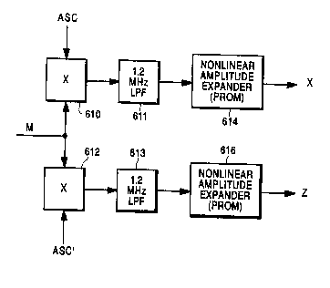
amplitude expander circuitry 326. FIGURE 6 is a block
diagram of the circuitry 326.
In FIGURE 6, the signal M is multiplied by the
signals ASC and ASC' in respective multipliers 610 and 612.
The output signals of the multipliers 610 and 612 are
low-pass filtered to 1.2 MHz by the filters 611 and 613 and
then applied to respective programmable read only memories
(PROMs) 614 and 616. The PROMS 614 and 616 are programmed
l~U~7~
-13- RCA 84,323
with an amplitude expansion function that is the inverse of
an amplitude compression function that was used in the
encoder to psycho-physically hide the second and third
component signals in the compatible composite signal. The
output signal, X, of the PROM 614 is the decoded second
component signal, the expanded high frequency components of
the side panel signals. The output signal, Z, of the PROM
616 is the decoded third component signal, the fre~uency
shifted high frequency luminance signaI components of the
wideband widescreen EDTV signal. The signal Z may be
processed further as described below in reference to an
alternative embodiment of the present invention.
Referring to FIGURE 3, the signal X is applied to
side panel compressor circuitry 328 which effectively
reverses the expansion of the side panel data performed by
the encoder circuitry. This operation produces a signal
NTSCH, which represents the high frequency components of
the side panel signals, restored to their proper time
relationship with a time compressed center panel signal
developed by a Y-I-Q format encoder 344, described below in
reference to FIGURE 9. The compressor circuitry 328 is one
application of a sample interpolator shown in FI~.U~ES 10,
10a, 10b, and 10c.
In FIGURE 10, sample values of a video input
signal, designated S in the FIGURE, which may be, for
example, the signal X, are applied to three serially
connected delay elements, 121~a through 1214c. Each of the
delay elements delays sample values applied to its input
port by one period of the clock signal CK4. The input
video signal and the output signals of each of the delay
elements 1214a through 1214c are applied to respective dual
port memories 1216a through 1216d. The sample values are
written into each of the memories as they are received
using address values provided by a pixel counter 1210. The
counter 1210 is reset by the horizontal line synchronizing
signal, HS, and incremented by the signal CK4. The signal
provided by the counter 1210 is applied to a PROM 1212
which generates a read address value for the memories 1216
13C~73~
-14- RCA 84,323
and an interpolation factor DX. The sample values stored
in the memories 1216 are provided in parallel to two
peaking filters 1220 and 1222. The filters 1220 and 1222
amplify the high freguency components of the sampled data
signals provided by the memories 1216, relative to the low
frequency components, by an amount, PX, that is derived
from the interpolation factox DX according to a functional
relationship stored in a PROM 1225. The peaked sampled
data signals, S'(N) and Sl(N+1), are applied to a two-point
linear interpolator 1230. The interpolator 1230 weigh-ts
samples of the signal S'(N~1) and S'(N) by DX and 1-DX,
respectively, and sums the weighted sample values to
produce the interpolated output signal. The peaking
filters 1220 and 1222 compensate for high frequency roll-
off in the interpolator 1230.
FIGURE 10a shows more detail of the peaking
filters 1220 and 1222 and the interpolator 1230. FIGURE
10b is a block diagram showing the structure of a finite
impulse response (FIR) filter 1240 which is a part of the
peaking filter 1220. FIGURE 10c is a graphical
representation of the function stored in the PROM 1225
which generates the peaking factor, PX, from the
interpolation factor DX.
As set orth above, the circuitry shown in
FIGURES 10 through 10c may be used for a variety of sample
value interpolation operation~. It may be used to compress
the signal X to align the high freguency components of the
side panel signals to the side panel pixel values produced
by the format encoder 344. It may also be used, as set
forth below in reference to the format encoder 344, to
process the first component of the EDTV signal to expand
the low frequency components of the side panel signals.
The type of function performed by the interpolation
circuitry is determined by the programming of the PROM
1212. If the read address value provided by the PROM 1212
increases more rapidly than the write address value applied
to its address input port, the interpolator circuitry will
perform a compression function. If, on the other hand, the
~3~07;~
-15- RCA 84,323
read address increases more slowly than the write address
value then the interpolator will perform an expansion
function. Whether the interpolator performs an expansion
function or a compression function and the value of the
expansion or compression factor used are determined by the
programming of the PROM 1212. One skilled in the art of
digital signal processing circuit design would be able to
program the PROM 1212 for a particular expansion or
compression function.
Referring to FIGURE 3, the signal NTSCH is
developed from the expanded side panel data in the second
component signal, X, of the EDTV signal using a compression
factor of 4.49. The signal NTSCH is applied to
luminance-chrominance separation circuitry 340 which
separates the luminance (YH) and chrominance components of
the signal NTSCH and demodulates the chrominance signal
component to obtain two color difference signal components
(IH and QH). The signals YH, IH and QH are applied to the
Y-I-Q format encoder 344 along with signals YN, IN and QN
developed ~rom the first component signal, N, by
luminance-chrominance separation circuitry 342. The
circuitry used or the luminance-chrominance separators 340
and 342 may be identical; exemplary circuitry is shown in
FIGURE 8.
In E'IGURE 8, the signal N or the sign~l NTSCH is
applied to a band-pass filter 1810 and to a delay element
1~12 which compensates for the processing dela~ through the
filter 1810. The filter 1810 used in this embodiment of
the invention is a horizontal-vertical-temporal (H-V-T)
band-pass filter such as that descri~ed in the
above-referenced Isnardi application. This filter includes
a combination of delay elements which delay the signal
applied to its input port by a number of sample times, by a
number of horizontal line periods and by a number of field
periods and circuitry to weight and combine the delayed
samples to produce a filtered chromiance signal.
Alternatively, the filter may be realized by combining a
conventional chrominance signal band-pass ilter, a
~30C~73~
-16- RCA 84,323
conventional line comb filter and a conventional frame comb
filter in cascade. The output signal of the filter 1810 is
a separated chrominance signal. This signal is applied to
the subtrahend input port of a subtractor 1813, the minuend
input port of which is coupled to receive the signal
provided by the compensating delay element 1812. The
output signal of the subtractor 1813 is the luminance
component signal, YN or YH.
The chrominance signal developed by the filter
1810 may be represented as a sequence of sample values, I,
Q, -I, -Q, I, Q etc. where I and Q indicate samples of the
I and Q color difference signals, and the signs of the
samples indicate sampling phase, not necessarily sample
polarity. This chrominance signal is applied to first and
second latches 1814 and 1816. The latch 1814 is responsive
to the I-phase clock signal, ICK, provided by the clock
generation circuitry 332 of FIGURE 3, to hold sample values
of the chrominance signal that represent the I color
diference signal component of the chrominance signal. The
latch 1816 is responsive to an inverted version of the
signal ICK, provided by an inverter 1822, to hold sample
values representing the Q color difference signal component
of the chrominance signal. The output signals provided by
the latches 1814 and 1816 are applied to respective twos
complementing circuits 1818 and 1820. The circuits 1818
and 1820 are controlled by a signal provided by a frequency
divider 1824 to complement alternate ones of the sampled
data I and Q color difference signals. The signals
provided by the circuits 1818 and 1820 are the demodulated
signals IN or IH and ~N or QH, respectively.
As set~forth above, the signals YH, YN, IH, IN,
QH and QN are applied to a Y-I-Q format encoder 344 where
they are combined to form widescreen signals YFo/ IF' and
QF'. ~xemplary circuitry which may be used as the format
encoder 344 is shown in FIGURE 9. In FIGURE 9, the first
component luminance and color difference signals, YN, IN
and QN, are applied to side panel - center panel separator
circuitry 1940. The circuitry 1940, which may, for
. .
-
13~i73~
-17- RCA 84,323
example, include a demultiplexer (not shown) and a pixel
counter (not shown) separates pixel values on each line
that represent the low frequency components of the side
pan~l signals from the samples that represent the center
panel signal. In this embodiment of the invention, samples
1-14 and 741 to 754 from each horizontal line represent the
side panel signal while samples 15 to 740 of each
horiæontal line represent the center panel signal.
The circuitry 1940 provides sampled data signals,
Y0, IO, and Q0, representing the compressed side panels.
These samples are applied to a time expander 1942 that
expands the signal in time by a factor of 6 to produce
signals YL, IL and QL. These signals represent the low
frequency components of the side panel signals, restored to
their original widescreen time relationship. The signals
YL, IL and QL are added in combiner circuitry 1946 to the
signals YH, IH and QH from separator 340 to generate
restored widescreen side panel signals YS, IS and QS.
The circuitry 1940 also provides sampled data
signals YE, IE, and QE which represent the time-expanded
center panel portion of ~he first component of the EDTV
signal. These signal~ are applied to a time compressor
1944 which compresses the sampled data signals in time by a
factor of 0.81 to generate restored widescreen center panel
signals YC, IC and QC.
The restored side and center panel signals are
recombined by a splicer 1960 to generate the complete
wid~screen luminance and color difference signals.
Circuitry suitable for use as the splicer 1960 is shown in
FIGURE 11. In FIGURE 11, the splicer is shown as including
a network 1410 for splicing the luminance center panel and
side panel signals, YC and YS, respectively to generate the
widescreen luminance signal, YFo. In addition, FIGURE 11
shows an I signal splicer 1420 and a Q signal splicer 1430
which have the same structure and operation as the
illustrated Y signal -splicer.
In the encoding operation, the center panel and
side panel signals are purposely overlapped by, for
13(~J73~
-18- RCA 84,323
ex~mple, ten samples to compensate for corruption of sample
values at the boundaries of the side and center panel
regions. This corruption which may occur in the expansion
and compression processes. If the panels did not have an
overlap region, the potentially corrupted samples would be
abutted against each other and a seam would be visible in
the reproduced image. An overlap region of ten samples has
been found sufficient to compensate for up to five
corrupted sample values.
In FIGURE 11, a multiplier 1411 multiplies the
side panel signal YS by a weighting function W in the
overlap regions, as illustrated by the associated waveform,
before signal YS is applied to an adder 1415. Similarly, a
multiplier 1412 multiplies the center panel signal YC by a
complementary weighting function ~l-W) in the overlap
regions, as illustrated by its associated waveform, before
the signal YC is applied to the adder 1415. These
weighting functions exhibit a linear ramp-type
characteristic over the overlap regions and have values
between 0 and 1. They may be realized, or example by a
combination o~ a sample counter (not shown) which addresses
a ROM containing sample values representing the weighting
functions. The output signal of the adder 1415 is the
spliced widescreen luminance signal YFo.
Reerring to FIGURE 3, in a first embodiment of
the invention, the signal YFo is presumed to be applied
directly to a digital to analog converter (DAC) 354 which
is responsive to the clock signal CK4 for producing a
widescreen luminance signal YO at an output terminal 355
and, to the luminance input terminal of a conventional
multi-channel VCR 358. The luminance signal YO has a
bandwidth of 5 MHz. This approximately conforms to the ~.2
MHz bandwidth of an NTSC luminance signal. The widescreen
signals IF' and QF' in this first embodiment of the
invention are applied to a conventional quadrature
modulator 348 which generates a sampled data widescreen
chrominance si~nal, CF'.
13C)~3~
-lg- RCA 84,323
Circuitry suitable for use as the modulator 348
is shown in FIGURE 12. In FIGURE 12, the circles at the
clock signal input terminals of latches 910 and 914
indicate that these latches are responsive to the
complement of the clock signal ICK. An inverting latch 916
includes a twos complementer in its output circuitry to
provide a complemented version of its latched value as its
output value. The operation of the circuitry shown in
FIGURE 12 is the inverse of that of the demodulator
described above in reference to FIGURE 8.
The signal CF' provided by the modulator 348 is
presumed to be applied directly to a DAC 356 which operates
in the same manner as the DAC 354 to provide an analog
wideband chrominance signal, C0, at an output terminal 357
and to the chrominance signal input terminal of the
conventional multi-channel VCR 358. As used in this
application, the term multi-channel VCR means a VCR which
accepts component signals for recording and which provides
the component signals as output signals during playback.
The currently available S-VHS and ED-Beta VCR are examples
of multi-channel VCR's.
The signals ~0 and C0 may be displayed directly
on a widescreen monitor or recorded, using the VCR, and
played baclc on a widescreen monitor. The image produced on
the widescreen monitor may be of lesser quality than the
image produced on an EDTV receiver such as that shown in
FIGURE 15, described below, since the circuitry shown in
FI~URE 3 ignores the third and fourth components of the
EDTV signal, which, respectively, include high ~requency
luminance information, and information which helps the EDTV
receiver to generate a high quality progressive scan image.
The third and fourth components of the EDTV signal are not
used by the circuitry shown in FI~URE 3 because the
information conveyed by these components currently cannot
be recorded on currently available S-VHS or ~D-Beta VCRs.
However, the information conveyed by the third
component signal, the high frequency luminance detail, can
be displayed on a widescreen monitor. Consequently, a
~3U073~
-20- RCA 84,323
first alternative embodiment of the circuitry shown in
Fl`GURE 3, which is described is an embodiment in which the
circuit elements 330, 334, 336 and 346 are included to
decode the third component and add it to the luminance
signal YFo to produce a wideband widescreen luminance
signal YF'.
The circuit element 330 is a decoder which
recovers the fre~uency-shifted luminance signal high
frequency components from the signal Z, provided by the
quadrature demodulator and amplitude expander circuitry
326. Exemplary circuitry for use as the decoder 330 is
shown in FIGURE 7. In FIGURE 7, the signal Z is applied to
a side panel, center panel separator 1710, which may
operate in the same manner as the separator 1940, described
above in reference to FIGURE 9. The separator 1710
separates samples, YHO, representing high freguency
components of the side panel signals from samples, YH~,
representing the center panel signal. The samples YHO and
YHC are applied, respectively, to time expander circuitry
1712, and time compressor circuitry 1714, which may operate
in the same manner as the respective circuitry 1942 and
1944 described above in reference to FIGURE 9. The signals
YHS and YHC, generated by the expander and compressor
circuitry 1712 and 1714, respectively, are applied to a
splicer 1716 which may be the same as the splicer 1960
described above in reference to FIGURE 9.
Referring to FIGURE 3, the signal provided by the
decoder 330 is applied to an amplitude modulator 334. The
modulator 334 multiplies the signal provided by the decoder
330 by the 5 MHz signal, fc, provided by the clock
generation circuitry 332 to restore the high frequency
luminance signal to its original band of freguencies. The
high frequency luminance signal provided by the modulator
334 is applied to a high-pass filter 336 which blocks
fre~uencies less than 5 MHz. This filter removes the
baseband component of the signal provided by the modulator
334. The output signal of the high-pass filter 336 is
applied to one input terminal of an adder 346, the other
~3~7~
-21- RCA 84,323
input terminal of which is coupled to receive the signal
YFo. The adder 346 combines the high frequency components
of the luminance signal (between 5.0 MHz and 6.2 MHz) with
the widescreen luminance signal YFo to generate a wideband
widescreen luminance signal YF'.
In this alternative embodiment of the inv~ntion,
the wideband widescreen luminance signal, YF' is applied to
the DAC 35~ to generate an analog wideband widescreen
luminance output signal as the signal Y0. This signal may
be used with the signal C0 to produce a high definition
widescreen picture on a wideband widescreen monitor.
Although, at present, thexe are no consumer VCRs which have
sufficient bandwidth to record the wideband signal, it is
contemplated that, if one is developed, the wideband signal
may be recorded in component form using either Y and C or
R, G, and B signals.
A second alternative embodiment of the invention
includes vertical interpolation circuitry 350 which
compresses the widescreen luminance and chrominance signals
to generate widescreen signals that produce a normally
proportioned image on a monitor having a conventional ~:3
aspect ratio. The signals produced by the system without
the vertical interpolator may be displayed on a 4:3
monitor, but the image produced would appear vertically
stretched.
FIGURE 13 illustrates the vertical compression
operation performed by the vertical interpolator 350. The
block on the le~t o FIGURE 13 represents a field of one of
the signals applied to the interpolator 350 and the block
on the right represents the same field after it has been
processed by the interpolator 350. As illustrated by
FIGURE 13, the interpolator maps the vertically stretched
information in the widescreen image, as it would be
displayed on a standard monitor, into a normally
proportioned image. The vertically compressed image
includes blanked areas above and below the active image
area.
13~73~
-22- RCA 84,323
FIGURE 14 is a block diagram of circuitry
suitable for use as the vertical interpolator 350. In
Figure 14, the luminance signal YF' is applied to an input
port of a one horizontal line period (lH) delay element
1450 and to a subtractor 1454. The subtractor 1454
subtracts samples provided by the lH delay element from
samples of the signal YF' and applies the sample difference
values to a multiplier 1456. The multiplier 1456 is
coupled to receive an interpolation factor from the eight
least significant bit (LSB) positions of an accumulator
register 1464. The scaled sample values provided by the
multiplier 1456 are added to the sample values provided by
the lH delay 1450 to generate interpolated sample values.
The register 1464 and adder 1462 form an
accumulator which determines which of the input lines are
to be averaged to produce the line of interpolated output
samples/ and what interpolating factor is to be used. The
register 1464 provides a 16-bit value to one input port of
an adder 1462. The other input port of the adder 1462 is
coupled to a digital value source 1460. The register 1464
is loaded synchronous with a loading signal that is the
logical AND of the enabling signal, EN, and horizontal
s~nchronization signal, HS. The register 1464 is reset by
the vertical synchronization signall VS. For each pulse of
the loading signal, the adder 1462 adds a value, 321, to
the value held in the accumulator register 1464, and then
stores the result iIl the register 1464. The eight most
significant bits (MSBs) of the value held in the
accumulator are the line number, NL, relative to the
vertical synchronization pulse, of the next line to be used
by the interpolator. The eight LSBs of the accumulator
value are the scale factor, K, to be used to generate the
interpolated line from the line of samples currently ~eing
applied to the interpolator and the line of samples stored
in the lH delay 1450. In this configuration, the
interpolator compresses the lines of samples applied to its
input port by a factor of 256/321 or 0.80.
~3~739
-23- RCA 84,323
The line number signal, NL, provided by the
registex 1464 is applied to one input port of a comparator
1490, the other input port of which is coupled to receive a
value provided by a counter 1488. The counter 1488 is
reset by the signal VS and incremented by the signal HS
and, so, holds the line number, relative to the vertical
synchronization pulse of the line of samples currently
applied to the interpolator circuitry 350. The comparator
1490 is configured to produce a logic one signal when the
signal NL is equal to the value provided by the counter
1488 and to provide a logic-zero otherwise. The output
signal of the comparator 1490 is the signal EN.
Responsive to the signals EN and CK4, the lH
delay element 1450 loads a new line of samples. Responsive
to the signals EN and HS, the accumulator 1464 increments
its value by 321 to indicate the next line of input samples
to be loaded into the lH delay element 1450 and to indicate
the factor to be used to interpolate the next ]ine of
output samples.
The interpolated sample values provided by the
adder 1458 are applied to the input port of a first-in-
irst-ouk (FIFO) memory 1466. The FIFO 1466 desirably has
a sufficient number of storage cells to hold samples
representing 40 lines of interpolated signal, corresponding
to the 40 lines of samples generated during the first and
last 24 active line intervals of each field of the input
signal. The output signal is blanked during ~hese 48 line
intervals. The FIFO 1466 is conditioned, by the signals EN
and CK4, to write samples provided by the adder 1458. The
FIFO 1466 is conditioned to provide stored samples at its
output port responsive to the signal CK4 and to a signal
D0.
Th~ signal D0 is generated by circuitry which
includes digital value sources 1494 and 1498, comparators
1492 and 1496, a NAND gate 1481 and a 24H delay element
1491. The signal D0 is in a logic-one state when the line
number value provided by the counter 1488 is between 44 and
238 and is in a logic zero state otherwise. Thus, the FIFO
~3~73~
- -24- RCA 84,323
1466 is conditioned to provide lines of samples only during
the unblanked active field interval of the vertically
compressed signal. The signal DO i5 delayed by 24
horizontal line periods by the delay element 1491 to allow
the lines at the end of a field to be interpolated before
they are provided as c)utput signal.
The sample ~alues provided by the FIFO 1466 are
applied to one input port of a multiplexer 1468, the other
input port of which is coupled to receive the composite
synchronization signal, CS, provided by the circuitry 332
of FIGURE 3 via a 24H delay element 1469. The multiplexer
1468 is controlled by the signal D0 to provide the
interpolated lines of samples from the FIFO 1466 during
lines 44-238 of each field interval and to provide the
composite synchronizing signal otherwise. This effectively
blanks the lines 20-43 and 238-262 of each field.
The circuitry which interpolates the chrominance
signal, CF ', ig similar to that described above for the
luminance signal, YF'. The chrominance signal
interpolation circuitry is different only because it must
accommodate for the 180 phase shift between successive
lines of the interpolated signal. Since the interpolator
does not use every line of input samples to generate lines
of output samples, it is possible that the two lines used
in the interpolation may have the same or opposite phases.
To ensure that the interpolation circui~ry always generates
correctly phased chrominance signals, the chrominance
interpolation circuitry includes an adder 1474,
corresponding to the subtractor 1454, and includes
selective twos complementing circuits 1478 and 1480 coupled
to the input ports of an adder 1482 corresponding to the
adder 1458. The circuits 1478 and 1480 selectively change
the polarity of samples applied to their input ports in
response to respective control signals A and B.
The control signals A and B are generated by
circuitry which includes two data-type (D) flip-flops 1483
and 1487, an exclusive-or gate 1485 and an inverter 1489.
The two flip-flops are configured as a two-bit shift
~ ~ .
~3VV7~
-25~ RCA 84,323
register that is clocked by the signal EN and that has the
LSB of the signal NL as its input signal. The output
signals of the flip-flops 1483 and 1487 indicate the
relative chrominance signal phases of the line of samples
held in the lH delay line 1470 and the line of samples
cuxrently being received. If the chrominance phases are
different, the signal ~ is a logic-one and the signal A is
a logic-zero. If the chrominance phases are the same, the
signal A is a logic-one and the signal B is a logic-zero.
When either of the control signals A or B is a logic-one,
the coxresponding twos complementing circuit 1483 or 1487
complements values applied to its input port, otherwise, it
passes the values unchanged. The remainder of the
circuitry in the chrominance interpolator operates
identically to corresponding circuitry in the luminance
interpolator.
~ eferring to FIGURE 3, the signals YI and CI
provided by the vertical interpolation circuitry 350
represent a widescreen image that has been vertically
compressed so that it will produce a properly proportioned
5:3 image on a conventional 4:3 display device. These
signals are converted to the analog signals ~0 and C0 by
the DACs 354 and 356 as set forth above. The signals Y0
and C0 may be applied to a conventional 4:3 monitor,
recorded on a conventional multi-channel VCR. The signals
Y0 and C0 may also be combined by, for example, a summing
network 360 to generate a composite video signal. This
composite video signal may be applied to a composite video
input terminal of a conventional single channel VCR, or
modulated by a modulator 362 to generate an RF television
signal which is applied to an RF input terminal of the
single channel VCR. As used herein, the term
single-channel VCR means a VCR which accepts only a
composite video input signal, such as a conventional VHS or
Beta machine.
The circuitry set forth above provides several
methods of processing an ~ncoded wideband widescreen
television signal to generate a widescreen and, in one
~3Qa;~3~
-26- RCA 84,323
instance, a wideband signal that is compatible with
existing recording and display apparatus. However, some of
the signals described above will only produce a properly
proportioned display on a widescreen monitor.
FIGURE 15 is a block diagram of a modification of
the EDTV receiver circuitry described in the above-
referenced Isnardi application. This modification allows
the EDTV receiver to be used as a wideband widescreen
monitor for displaying images developed from component
luminance and chrominance signals. The circuitry shown in
FIGURE 15 includes an EDTV decoder that is similar to the
one described above in reference to FIGURE 3. The decoder
of FIGURE 15 di~fers from that shown in FIGURE 3 because
the input unit 1322 includes a synchronous detector and ADC
which recover the quadrature phase modulation component of
the RF video signal, i.e. the fourth component of the EDTV
~ignal, YTN, and a format decoder 1360 which reverses the
mapping operation that was used to psycho-physically hide
the fourth component signal in the compatible composite
signal. The circuitry shown in FIGURE 15 also includes
interlace scan to progressive scan converters 1350, 1352
and 1354 ~o~ the luminance and color difference signals
provided hy a Y-I-Q format encoder 1344, a DAC 1362, signal
processing ci~cui~r~ 1364 and display apparatus 1370.
Th~ EDTV receiver is converted to an EDTV monitor
by switches 13~8, 1390, and 1392 inserted in the respective
luminance and r and Q color diference signal paths from
the ormat decoder 1344 to the respective interlace to
progressive scan converters 1350, 1352 and 1354, and by a
switch 1380 in the signal path between the format decoder
1360 for the fourth component V~T helper signal, YT, and
the interlace to progressive scan converter 1350. In
addition to the above, the converter 1350 is modified to
compensate for the lack of a V-T helper signal when the
EDTV receiver is used as a monitor.
The switches 1388, 1390 and 1392 are controlled
by a signal O/R, which may be provided through an external
mode switch (not shown) on the receiver, to pass luminance
-27- 0739 RCA 84,323
and color difference signals provided by the format encoder
1344 or to pass a luminance signal provided from an input
terminal, YR, by an ADC 139~ and I and Q color difference
signals provided from an input terminal, CR, by an ADC 1398
and a conventional chrominance signal demodulator 1394.
The switch 1380 is conditioned by the signal O/R to provide
either the decoded ~ourth component signal, YT, or a zero
value from a digital value source 1382.
The signals IF' and QF', provided by the
respective switches 1390 and 1392, are processed by the
interlace to progressive scan converters 1352 and 1354 in
the same manner whether they originate from the decoder or
from an external source. FIGURE 16 is a bloc~ diagram of
an interlace to progressive scan converter suitable for use
as either o~ the converters 1352 or 1354. In Figure 16,
the interlace signals IF' (or QF') are delayed 263H by an
element 2010 before being applied to an input port of a
dual port memory 2020. This delayed signal is subjected to
an additional 262H delay by an element ~012 before being
added with the input signal in an adder 201~. The output
signal from the adder 2014 is coupled to a divide-by-two
network 2016. The output signal of the network 2016 is
applied to an input port of a dual port memory 2018.
Memories 2020 and 2018 write data at a 4fsc rate and read
data at an 8fsc rate. The output signals provided by the
memories 2018 and 2020 are applied to a multiple~er 2022
which produces an output progressive scan signal, IF (QF).
Also shown in FIGURE 16 are waveforms which illustrate the
interlace scan input signal (two lines, with pixel samples
C and X designated) and a progressive scan output signal
which includes the samples C and X.
FIGURE 17 is a block diagram of circuitry
suitable for use as the luminance signal interlace to
progressive scan converter 1350. The circuitry shown in
FIGURE 17 operates in two modes. When the signal O/R
indicates that the luminance input signal, YF', is provided
by the decoder, the circuitry in FIGURE 17 operates in the
same manner as that shown in FIGURE 16 except that the
-28- RCA 84,323
fourth component V-T helper signal is added to the frame
averaged signal provided by a divider 2116 to provide an
input signal for a dual port memory 2122. However, when
the signal 0/R indicates that the signal YF ' is provided
from the external input terminal, YR, the circuitry shown
in FIGURE 17 switches between operating identically to the
circuitry shown in FIGURE 16 when a still image is being
displayed and operating as a line-repeat interlace to
progressive scan converter when a moving image is
displayed. This change in operational mode is implemented
by the addition of a conventional interframe motion
detector 2126 and a switch 2128.
The motion detector 2126 is responsive to the
signal 0/R to be active only when the luminance signal YF'
is from the input terminal YR. The detector 2126 compares
corresponding pixel values separated by one frame interval.
If the pixel values are substantially equal, then there is
no motion in the image at the pixel position and, so, the -
switch 212~ is conditioned to pass the output signal of the
divider 2116 to the input port of the memory 2122. If the
detector 2126 finds a significant difference ~etween the
pixel values, it conditions the switch 2122 to apply the
same signal to the memory 2122 as is applied to the memory
2120. The samples provided by the output multiplexer 2124
of the luminance signal interlace to progressive scan
converter are frame averaged signals for still portions of
the image and vertically repeated signals for moving
portions of the image.
Referring to FIGURE 15, the signals generated by
the interlace to progressive scan circuits 1350, 135~ and
13S4 are converted into respective analog Y, I and Q
signals by the DAC 1362. These signals are applied to the
video signal processor and matrix amplifier unit 1364. The
video signal processor part of the unit 1364 includes
signal amplifying, VC level shifting, peaking, brightness
control, contrast control and other conventional video
signal processing circuits. The matrix amplifier part of
the unit 1364 combines the luminance signal Y with the
-29- ~30V~39 RCA 84,323
color difference signals I and Q to produce primary color
signals R, G, and B. These primary color signals are
amplified by display driver amplifiers in the unit 1364 and
used to drive the widescreen color image display device
1370 which may be a widescreen kinescope.
Although the various embodiments of the present
invention set forth above in reference to FIGURES 3 and 15
are described separately, it is contemplated that they may
be used in virtually any combination to provide a variety
of methods for displaying and recording a wideband
widescreen EDTV signal.