Note: Descriptions are shown in the official language in which they were submitted.
L3~J!07~t~
-1- RCA 84,941
VIDEO SWITCHING APPARATUS HAVING
INTERFERENCE PREVENTION FEATURE
This invention relates to switching apparatus for
use in a video signal processing system.
In a standard color television receiver, a
composite video baseband signal (CVBS) derived from the
receiver's video detector stage is applied to a luma/chroma
separator, which separates the composite video signal
(CVBS) into a luma component (Y) and a chroma component
(C). In the NTSC format, the bandwidth of the luma
component recovered from a composite video baseband signal
is about 4.2 MHz (or 330 lines of horizontal resolution).
Recently, higher definition TV sys~ems (e.g.,
S-VHS and ED~BETA) have been introduced that provide
alreadv-separated luma and chroma, or Y/C signals. A
feature of these new systems is that the luma signal has a
considerably wider bandwidth (as compared to a 4.2 MHz
bandwidth of a luma signal derived from an NTSC composite
video baseband signal). Illustratively, the luma signal
provided by the S-VHS system has a bandwidth of about 5.1
MHz ~i.e., 400 lines of horizontal resolution). The luma
signal provided by the ED-BETA system, on the other hand,
has a bandwidth of about 6.4 MHz (i.e., 500 lines of
resolution).
Typically, a standard color TV receiver is not
equipped to handle these externally-supplied wideband luma
and chroma signals. It is possible to combine these
externally-supplied wideband Y/C signals into a composite
video baseband signal in the NTSC format, and apply it to
the receiver's luma/chroma separator. Because the
luma/chroma separation process is inevitably imperfect in
practice, there is always some possibility of cross
contamination. The presence of the luma signal in the
chroma channel is known as cross-color. The presence of
the chroma signal in the luma channel manifests itself as
hanging or crawling dots on the TV screen.
In accordance with this invention, a video
selector or Y/C switch is provided which has input terminals
, .
-` 130()74(~
-2- RCA 84,941
for receiving in~ernally-separated luma and chroma signals,
as well as externally-supplied wideband luma and chroma
signals. The video switch selects a pair of input
component signals for application to its output terminals
in response to a control signal. Means are provided for
disabling the luma/chroma separator circuits when the video
selector switch selects a pair of externally-supplied
component signals for application to its output terminals.
IN THE DRAWINGS:
FIGURE 1 provides a block diagram of a
conventional TV receiver to illustrate the environment in
which the subject invention is used;
FIGURE 2 is a block diagram of an integrated
circuit that incorporates a YtC selector switch and
separator disabling means in accordance with the principles
of the present invention; and
FIGURE 3 iS an alternative arrangement of the
FIGURE 2 disabling means.
In the drawings, the lines interconnecting
various blocks represent either single conductor
connections carrying analog signals or buses carrying
binary digikal signals, as the case may be. A value next
to a slash mark intercepting a particular interconnecting
line represents the number of parallel connections of that
line or bus.
Dependin~ on the processing speed of the devices
used, compensating delays may be required in certain of the
signal paths. One skilled in the art of digital video
signal processing circuit design would know where such
30 delays would be needed in a particular system.
As shown in FIGURE 1, a television (TV) receiver
10 is provided with an input terminal 12 for receiving a
radio frequency (RF) signal from an antenna or a cable
system. The RF signal is applied to a plurality of
receiving circuits 1~ including a tuner, intermediate
frequency (IF) circuits and a video detector stage. A
composite video baseband signal CVBS from the video
3C~
-3- RCA 84,941
detector stage is applied to a luma/chroma separator 18.
The luma/chroma separator 18 separates the composite video
slgnal CVBS into a luma component Y and a chroma component
C. In the NTSC format, the bandwidth of the luma component
recovered from a composite video baseband signal i9 about
4.2 MHz (or 330 lines of horizontal resolution).
A luma/chroma processor 24 translates the luma
and chroma component signals Y and C into a set of red,
green and blue picture tube drive signals R, G, and B. The
R, G and B signals are amplified by an output stage 26 and
applied to a picture tube 28.
A block 30, coupled to receive the composite
video signal CVBS, includes the sync separator and
deflection circuits. The circuits 30 develop a pair of
horizontal and vertical deElection signals HDS and VDS.
The horizon~al and vertical deflection siqnals HDS and VDS
are applied to a pair of de1ection windings 32 disposed
about the neck portion of the picture tube 28.
The kinescope 28, coupled to receive the red,
green and blue drive signals R, G and B and responsive to
the horizontal and vertical de1ection signals HDS and VDS,
produces color images on a screen 34.
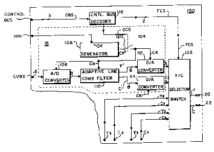
Shown in FIGURE 2 is an integrate~ circuit 100,
which houses a Y/C selector switch 102 and disabling means
104 in addition to the FIGURE 1 luma/chroma separator 18.
For the purposes of description, the luma/chroma separator
18 is assumed to include a digital comb ilter.
Alternatively, the luma/chroma separator 18 could be a
charge coupled device (CCD) comb filter.
The digital comb filter 18 includes a circuit 106
for generating a burst-locked system clock signal CK. The
frequency FCK of the clock signal CK is established at 4
times the frequency FSc of the color subcarrier signal
component (i.e., color burst) of the composite video signal
CVBS. Additionally, the clock signal CK is phase locked to
the color burst signal.
An analog-to-digital (A/D) converter 108
translates the composite video signals CVBS into 8-bit
~30~740
4 RCA 84,941
binary digital samples at instants determined by the clock signal
CK. The digital samples from the A/D converter 108 are applied
to a digital comb filter 1 10. The filter 1 10 separates the incoming
stream of digital samples into samples representative of the luma
component Y'l and samples representative of the chroma
component C' 1-
A pair of digital-to-analog converters 112 and 114
convere the digital luma and chroma samples Y'l and C'1 into
corresponding analog representations Y1 and C1 thereof. The
digital comb filter circuits 106-1 14 are of the type described in
greater detail in ~J.S. Patent No. 4,786,963 of McNeely et al. and
entitled "AD~P1'IVE Y/C SEPAR~TION APPARATUS FOR TV
SIGNALS".
The analog luma and chroma component signals Y 1
and C1 are applied to a first pair of input terminals of the video
selector switch 102. The switch 102 is further equipped with
second and third pairs of input terminals for receiving externally-
supplied wideband componerlt signals Y2, C2 and Y3, C3.
The component signals Y2, C2 and Y3, C3 are of the type
supplied by an SVHS video cassette recorder. As previously
indieated, externally-supplied luma signal components Y2 and Y3
may be wiclebancl signals, with bandwiclths tllat may extend well
beyond the bandwiclth of the internally-getlerated luma signal
eomponent Yl.
2 5 The video switch 102, responsive to a 2-bit first
eontrol signal FCS, seleets one of the three sets of input component
signals ~1/Cl, Y2/C2 atlCl Y3/C3 for applieation to a pair of output
terminals 20 and 22. The luma and chroma signals Y and C from
the output terminals 20 and 22 of the video switch 102 are
3 0 applied to the luma/chroma processor 24.
The IC 100 is equipped with a control bus decoder
116, which provides the first control signal FCS in response to a
three-wire user-controlled serial-bus signal CBS. The Y/C selector
switch 102 responds to the control signal FCS. Illustratively, the
3 5 switch 102 selects the first, second and third pairs of component
signals Yl/C1,
3L30~7~0
...
-5- RCA 84,941
Y2tC2 and Y3/C3 when the first control signals is 01, 10
and 11 respectively~ The Y/C selector switch 102 sends no
output to the output terminals 20 and 22 when the first
control signal FCS is 00.
The control bus decoder 116 additionally provides
a second control signal SCS for disabling the circuitrv 18
used for decodinq the composite video signal CVBS into its
components when the selector switch 102 selects a pair of
externally-supplied component signals for application to
the luma/chroma processor 24. To this end, an electronic
switch 120 is interposed between the clock generator 106
and the rest of the digital processing circuitry 18. When
the switch 120 is opened, the A/D converter 108, the comb
filter 110 and the D/A converters 112 and 114 are shut off
or deactivated.
FIGURE 3 shows an alternative arrangement for
disabling the composite signal decoding circuit 18. As
shown, therein, a switch 120', responsive to the control
signal SCS, is interposed between a DC operating voltage
VDD and the clock generator 106. When the switch 120' is
opened, it turns off the clock generator 106. When the
clock is turned off, all the clock-driven circuits 108-114
are also shut off.
An advantac~e of this invention is that it
prevents the intererence from the clocked circuits 18 from
coupling into the externally-supplied wideband component
signals Y2 and Y3, when the Y/C selector switch 102 selects
a pair of externally-supplied component signals for
application to its output terminals 20 and 22. As
previously indicated, the bandwidth of these
externally-supplied component signals is sufficiently wide
(e.g., 6.4 MHz) to make them susceptible to cross-talk from
the clock-driven circuits 18.
In the embodiment described and shown herein, a
digital comb filter 18 is used for separating a composite
video signal CVBS into its luma and chroma components Y
and Cl. The composite video signal CVBS is sampled at
instants determined by the clock signal CK and quantized
~. .
'` .,~. '
:,
~ ~3~)~7~
-6- RCA 84,941
into 8-bit binary digital samples. However, the present
invention is not limited to digital signal processing. As
indicated before, it is equally applicable to a composite
signal decoding system using a CCD comb filter. In a CCD
comb filter, a composite video signal CVBS is sampled in
response to a clock signal, but is not quantized into
binary digital values.
Furthermore, in the embodiment shown and
described, the Y/C selector switch 102 is coupled to
receive the analog component signals Yl/Cl, Y2/C2 and
Y3/C3. Alternatively, the Y/C selector switch 102 could be
designed to receive digital component signals.