Note: Descriptions are shown in the official language in which they were submitted.
3~0755
83-447
--1--
~ACl~GRC)UND OF TEIE INVENTION
1. Field of the Inventio_
The invention relates generally to the field of digital
data processing systems, or computer systems, and more
specifically to computer workstations.
2. Background
Untll recently, computer systems were large, expensive
ma~hines, generally too expensive to devote an entire
computer system to one person. However, with the
development of large and very large scale integrated circuit
technology, which in turn provided the microprocessor,
providing a computer s~stem to one person has become cost
ef~ective. Personal computers and the more advanced
computer workstations permit one person to have sole access
to his or her computer for many kinds of activities,
including word processing, accounting and financial
planning, and computer aided design and engineering. In
many cases, the personal computers and workstations are
connected over a network to a laryer minicomputer or
~30075~;
83-447
--2--
mainframe which provides large scale data storage and data
hase management capabilities and manages such auxiliary
equipment as printers and telecommunication interfaces.
These arrangements permit sharing of information among users
working on the personal computers and wcrkstations. In
addition, the larger computer may perform complex or lengthy
arithmetic calculations, such as recalculating spreadsheets
and processing of engineering simulations.
A computer workstation generally includes a processor,
a memory, au~iliary storage such as disk storage, a keyboard
~or usee data entry and a video display or displaying
output to th~ user. In addition, i the workstation is to
be us~d in a network, a network interface will also be
included. The processor includes a microprocessor chip and
may also include one or more auxiliary proce~60r chips for
processing special classes of instructions, most notably
floating point insteuctions. The memory includes a read
only portion ~ROM) which generally includes the boot portion
of the opcrating ~ystem, read/write random access memory
(RAM) which is used for program instruction and data
storage, including the remainder-of the operating ~ystem,
13~ 83-447
--3--
and a video RAM which stores data depicting the image do be
displayed on the video monitor.
When the workstation is initially turned on, the
proce~sor initially operates in response to bootstrap
in6tructions from the boot ROM, and enables the remainder of
the operating system and other programs and program data to
be loaded into the RAM from the disk storage devices.
~uring subsequent program execution, the processor may write
data to be displayed into the video RAM. The network
interface i5 al~o connected to the RAM to enable data from
the network to be loaded therein or data to be retrieved
there~rom or transmis6ion over the network. Circuits for
controllin~ the video display read the data out of the video
RAM and in response to ~he data generate video signals which
are coupled to the video display. Based on the video
~ignals, the video display generates an image for the user.
The processor, disk storage devices, network interface
and video control circuits are all connected to write data
to or retrieve data from one or more portions of the memory.
A (User input through the keyboard is typically handled as a~
- interrupt serviced by the processor rather than as a direct
transfer to memory.) All portions of the memory, that is,
- 83-447
--4--
the boot ROM, the ~AM and the video RAM typically occupy a
~ingle address space, that is, the addresses of the
locations in the boot ROM, RAM and video RAM do not overlap.
In addition, the disk storaqe devices and network interface
typically include control and status registers which also
occupy a portion of the same address space. Thus, if the
processor, for example, wishes to perform a transfer with
any storage location in the boot ROM, RAM, video ~AM or any
of the control and status registers in the disk devices or
network interface, the address transmitted by the processor
during the transfer comple`tely identifies the location.
The video image displayed by the video display unit is
in "real time", that is, the generation of the image cannot
be delayed without disrupting the image as seen by the
viewer. Accordingly, the video control circuitry must be
able to retrieve data rom the video RAM in a timely manner.
~owever, acces6 to the memory can be impeded by memory
requests from the proces60r~ disk devices or network
interface. Typically, a workstation includes an arbitration
mechanism wh~ch arbitrates memory requests among the various
devices, that is, the processor, video control circuitry,
network interface and disk storage devices, which may be
07$5
~ 6822-62
requestiny access to memory. However, this requires a complex
mechanism to ensure that the video control circuitry has access
to the memory, and specifically the video RAM in a timely
manner to ensure that the image on the video display is not
disrupted.
SUMMARY OF THE INVENTION
The invention provides a new and improved computer
workstation which ensures that the video control circuitry has
timely access to the video RAM.
In brief summary, the new workstation includes a
processor and lnput/output devices such as disk devices and/or
networ~ interfaces, and a master control circuit that controls
accesses to a common memory which includes a video memory and
enables transfers of video information from the video memory as
re~ulred to ensure uninterrupted display on a monitor. The
processor determlne.q which unit, among it~elf, the disk devices
or the net~ork interface will be ahle to perform a transfer
operation with memory. The master control circuit inhibits
other units from accessin~ the memory while it is in the
process of enabling transfers of video information from the
video memory.
More particularly, according to one aspect the
invention provides a computer system comprising: A. video
information storage means for storing video informa~ion in a
plurality of video information storage locations, æaid video
information storage means including video address inpu~ means,
video information input means, and video information output
means; B. video means connected to said video information
output means for receiving video information from said video
information storage means for display; C. a plurality of
utilization means, all of which are connected to said video
information input means and said video information output
s
~.~
`` ~300~7SS
66822-62
means, for transferring video information to and from said
video information storage means, said utilization means
in~luding video address transmitting means for providing a
video address, video information transmitting means connected
to said video information input means for providing video
information to said video information input means for storage
in said video information storage locations, and video
information receiving means connected to said video information
outpu~ means for receiving video information; D. arbitration
10 means connec~ed to all of said utilization means for enabling
one of said ukllization means to perform a video information
transfer with said video i~formation storage means; and
E. access aontrol means connected to all of said utilization
means, includingl ~. address stora~e means connected to the
: video address transmitting means in said utilization means for
lat~hin~ the video address provided from the one of said
utillzatlon me~ns enabled by saicl arbitration means; ii. video
update addxess generation means ~or generating a video address;
iii. coupling means ~onneated to said address storage means and
20 said video update address generation means for selectively
coupling the video address latched in said address storage
means or the video address generated by said video update
address generation means to said video address input means of
: said video information storage means; iv. control means,
connected to said coupling means, said address storage means
and said video update address generation means, for controlling
said coupling means to normally transfer the video address
latched in said address storage means to said video address
input means, for providing video transfer control signals to
enable a transfer of video information between one of said
plurality of utiliæation means and a storage location in said
video information storage means identified by tha video address
5a
~3(~075X
66822-62
latched in said address storage means, for controlling said
coupling means to transfer the video address generated by said
video update address generating means, for providing video
update control signals to enable a transfer of video
information from the storage location identified by the video
: address generated by said video update address generation means
to said video means to theraby perform a video update
opera~ion, and for inhibiting access by said utilization means
to said video information storage means during the video update
operation; and v. timer means for generating a video update
timing signal to enable initiation of the video update
operation, whe.rein sald control means lnltiates the vldeo
update operatlon in response to generation of said video update
timlng signal.
~ ccording to another aspect the present invention
provides a digital computer system, comprising, memory means
for storiny dig~tal informatlon in a plurallty of addressable
storage locatlons, said lnformatlon lncluding program data
stored in program data storage lo~atlons and video data stored
in vldeo data storage locations; address receiving means,
including in sald memory means, for receiving an address
identifying a storage location; memory control signal receiving
means, included in said memory means, for receiving memory
control signals; video means, operatively coupled to said
memory means, for receiviny video data from said ~emory means
for display; a plurality of memory utilization means,
; operatively coupled to said memory means, for tra~sferring
information to and from said memory means; arbitration means,
operatively coupled to said plurality of memory utilization
means, for enabling one of said memory u~ilization means to
initiate an information transfer with said memory means; global
timing means for generating a global timing signal; memory
5b
~ ~755i
66822-62
control means, operatively coupled to said memory means and
said plurality of memory utilization means, for controlling
access by said plurali~y of memory utilization means to said
memory means, and for controlling said memory means to transfer
the video data stored in a predetermined portion of said video
data storage locations to said video means; wherein said memory
control means includes video address generating means for
generating a video address that identifies the predetermined
portion o~ said video data storage locations that contain video
data to be transferred to said video means, coupling means,
operatively coupled to said video address generatlng means and
said address receiving means, for coupling the video address
generated by said video address generating means to said
address re~eiving means, video timer means, operatively coupled
to receive the global timing signal, for generatiny a video
transer enable slgnal, an~ control circult means, responsive
to sald vldeo transfer enahle signal and operatively coupled to
sald video aclclress generating means, said coupling means, said
memory means, and said video means, for providing a first
control signal to cause said memory means to transmit to said
video means the video data skored at the predetermined portion
of said video data storage locations identified by the video
address generated by said video address generatlng means, for
providing a second control signal to cause said video means to
receive the video data, and for inhibiting access by said
memory utllization means to said memory means whlle video data
-~ is transferred from said memory means to said video means.
'
5c
r.;l
:
~W7~;S 83-447
--6--
RISF DESCRIPTION_OF THE DRAWINGS
Thi~ invention is pointed out with particularity in the
appended claims. The above and further advantages of this
invention may be better understood by referring to the
following description taken in conjunction with the
accompanying drawings, in which:
Fig. l depicts a general block diagram of a computer
workstation constructed in accordance with the invention;
Fig. 2 depicts a functional block diagram of a master
control circuit in the computer workstation depicted in
Fig. 1.
DETAILED DESCRIPTION OF AN ILLUSTRATIVE EME~ODIIIIENT
A computer wo~kstation constructed in accordance with
the lnvention i8 ~hown, in general block diagram form, in
Fig. 1. With re~erence to Fig. 1, the workstation includes
a processor 10 including a central processor unit (CPU) 11
and floating point accelerator processor 12 which transfer
addresse~ and data, including such information as program
instructions and program data, with other unit~ in the
system through a buffer 13. The floating point accelerator
-` i3~075S
83-447
--7--
proce~sor 12 is provided to accelerate processing of
floating point instructions. The processor 10 generates and
transmits a free-running SYS CLR system clock ~ignal to
synchronize events in the workstation. In one embodiment,
the processor 10 operates in synchronism with a multiple
phase clock, with the ticks of the SYS C~K system clock
~ignal (that is, the successive leading edges of the SYS CLR
system clock signal) defining the ticks of the successive
phases of the processor's multiple phase clock.
The workstation also includes a read/write random
access memory 20 containlng a plurality of addressable
storage locations for storing varia~le program instructions
and data. ~ read only memory 21, which also contains a
plurality o addressable storage locations, stores fixed
program instructions, including a bootstrap program and
selected portions o the operating system such as service
routines used in servicing interrupt requests from, for
example, input/output devices such as one or more disk
devices 23 or a network interface 24 which may be included
the system. The read only memory 21 also stores, at
predetermined locations, a plurality of interrupt vectors
14. Each interrupt vector identifies the location, in
~30~7~5 83-447
--8--
e~ther random access memory 20 or read only memory 21, of an
interrupt service routine for servicing an interrupt request
from units requiring interrupt service from the processor
10.
~ 5 i8 conventional, the system may also include other
input/output devices, such as ~erial or parallel
communications devices ~not shown) which transfer
inormation to or from the pu~lic telephone network and to
printers ~or providing a hard copy output. Transfers to and
from these devices are performed in a similar manner a~
tran~fers to and from the disk devices 23 and networ~
interace 24, and so these additional devices will not be
described further here.
In additlon, a read/write random access memory serves
as a video memory 22 to store, also in addressable ~torage
locations, video data detaillng an image to be displayed on
a video mon~tor (not shown). In one ~peciic embodiment,
the video ~emory 22 contains a "bit-mapped" representation
of the image to be displayed on the video display, that is,
the data bits stored in the addressable locations In the
video memory 22 have a direct correspondence to the
individual picture elements (pixels) displayed.
13~7S5 83-447
_g_
A~ descrlbed below, the processor 10 can read the
information ~tored in addressed locations in the random
access memory 20, read only memory 21 and through a driver
27, video memory 22, and it can also write information to
addre6sed location6 in the random access memory 20 and~
video memory 22.
In addition, periodically the information stored in a
plurality of sequential locations in the video memory 22 is
transferred in parallel form at one time to a shift register
25 to update its contents. Shift register 25 shifts its
contents out in serial form to conventional video display
control circults (not shown) in response to a VSR SCLK video
shlft register shift clock signal from the video display
control circuits. In cesponse to the contents of the video
shift register 25, the video display control c~rcuits
generate in a known manner video signals which control the
video monitor and are displayed as an i~age.
It wlll be appreciated that the driver 27 serves to
isolate the'data out"terminals of video memory 22 and, more
particularly, the data in''terminals of video shift register
25 from the data/address lines 15, since, as will be
described in more detail below, the data/address lines 15
~3~755
83-447
--10--
may have signals thereon during a video shift register
update operation.
The processor 10 can also read information stored in
control and status registers (not shown) in the dlsk devices
23 and network interface 24 and transfer information to such
registers to control the respective unitsO The control and
status registers are, like the storage locations in the
random access memory 20, read only memory 21 and video
memory 22, identified by addresses. In response to selected
conditions, such as the detection of an error or the
completion of a disk read or write operation7the disk
devices 23 may assert a DISR INT REQ disk interrupt request
signal. In addition, at the end of a network transfer, the
network interface 24 may assert a NET INT REQ network
interrupt request signal. The disk devices 23 may also
assert the DISK INT REQ disk interrupt request signal during
a disk storage operation to request the processor to
transfer data to it from the memory 20, or to transfer data
from it to the memory 20.
In addition, during the video monitor~s vertical
blanking interval, during which the electron beam is
returned from the bottom of the video screen to the top of
- - ~
~3007S5
66822-62
the video screen, the processor 10 is interrupted by a VERT BLK
vertical blank interrupt request signal. In response to the
VERT BLK vertical blank in~errupt request signal, the processor
10 performs certain housekeeping operations as described below.
The master control circuit 30 receives ~he DISK INT REQ disk
interrupt request, NET INT REQ network interrupt request, and
; VERT BLK vertical blank interrupt request signals and at an
appropriate time interrupts the CPU 11.
In addition, other units such as the aforementioned
serial and parallel communications devices (not shown)
typically also generate interrupt request signals to permit the
proce~sor 10 to per~orm selected operations therewith. The
operations normally performed by a processor 10 for such
devices are well known in the art and will not be described in
detail.
The buffer 13 in processor 10 buffers transmissions
of data and adtlress informatioll between the CPU 11 or floating
point accelerator processor 12 and a set of data/address lines
(DAL) 15. The data/address lines 15 are used to kransfer data
and address information from protessor 10 duriny a write
operation with other units in the system,
. i3~07~ 83-447
-12-
that is, during a transmis6ion to one of the memories 20
through 22, or to a control or status register in disk
devices 23 or network interface 24. In addition, the
data/address lines 15 are used during a read operation to
return read data from the storage location or register
identified by an address which is also transmitted by
processor 10 over the data/address lines 15. In one
embodiment, thirty-six data/address lines 15 carry, in
parallel, thirty-two information signals, which comprise
four eight-bit bytes of information, and four parity signals
(one associated wlth each byte) which are used in error
detection.
As is typical, the network interface 24 is a direct
memory access ( DMA) device. That is, network lnterface 24
retrieves data directly from, in particular, random access
memory 20 for transmission over a network (not shown). In
addition, network interface 24 transmits data received from
the network directly to random access memory 20 for storage
therein.
The disk devices 23 may also comprise a direct memory
access device, but in the embodiment described herein ~
not. Instead, the processor 10 initiates the transfer of
1300755 G3-447
-13-
data to or from the disk devices ~3 in response to an
interrupt therefrom.
To initiate a DMA operation, the network inte~face 24
asserts an NET DMR network direct memory request signal. In
response a DMA control circuit 26 asserts a DMR direct
memory request signal which i6 transmitted to the processor
10. When the processor 10 is to grant a direct memory
operation, it asserts a DMG direct memory grant signal,
which is received by the DMA control circuit 26. The DMA
control circuit then asserts the NET DMG networ~ direct
memory grant signal which enables the network interface 24
to engage in a DMA operation. I other devices are
connected into the system which transfer data with memory 20
ln a direct memory access manner, the ~MA control circuit
also r~ceives device direct memory request signals therefrom
and transfers device direct memory grant signals thereto.
If more than one request slgnal is asserted when the
processor 10 as~erts the D~G direct memory grant signal, the
D~A control circuit 26 asserts one o the device direct
memory grant signals based on a predetermined priority in a
conventional manner.
r~
` ~3~07SS
83-447
-14-
~ ike the processor 10, during a DMA operation the
network interface 24 provides addresses to identify the
location from which data is being retrieved or into which
data i8 being written. DMA operations occur under control
of control information in the control registers in the
re6pective units which is provided by processor 10, but
without intervention by processor 10 while the operation6
are occurring. AS is conventional, at the end of a transfer
operation, the unit asserts its NET INT REQ network
interrupt request signal to request interrupt service by the
proce~sor 10.
In accordance with the invention, a master control
circuit 30 controls the timing of transfers initiated by
processor 10 with random access memory 20, read only memory
21 and vidao memory 22, and the control and status register6
o disk devices 23 and network interface 24 over
data~address lines lS. In addition, the master control
circult 30 controls refresh of the random access memory 20
and video memory 22 and the transfer o video information
from thc video memory 22 to the shift register 25 during a
video shift register update ope.ration. The master control
circuit 30 further controls the timings of DMA transfers
~ ~3~755
83-447
-15-
between the network interface 24 and random access memory
20. If a video shift register update operation i6 enabled,
the master control circuit 30 holds off other operations
which may be initiated by the processor 10 or network
interface 24 until the video shift register update operation
and 6ubsequent refresh operations have completed. After the
video ~hift register update operation has been completed,
the master control circuit 30 enables other operations with
memory to proceed from the appropriate cycle of thq SYS CLK
system timing signal.
Finally, the master control circuit receives interrupt
request signals, such as the DISK INT RE~ disk interrupt
reguest, NET INT REQ network interrupt re~uest and VID INT
~EQ video interrupt request signals, and other interrupt
.request s~gnals ~rom other devices ~not shown) which may be
in the system, and transmits a single IN~ REQ interrupt
request signal to the processor 10. In response to a later
interrupt acknowledge transaction, as described below, from
the processor 10, the master control circuit enables the
transfer of an interrupt vector from the read only memory 21
to the processor 10. The master control circuit 30
establishes an interrupt priority among the various units
~.3~11755
83-447
: -16-
which generate interrupt request signals, and lf more than
one unit is a~serting an interrupt request signal when the
processor 10 initiates an interrupt acknowledge transaction,
the master control circuit 30 enables the transfer of the
interrupt vector a~sociated with the unit having the highest
priority who6~ interrupt request signal is asserted.
The processor 10 or networ~ interface 24, to initiate a
transfer with a memory unit, tha`t.i~, either the random
access memory 20, read only memory 21, or video memory 22,
first places address signals on data~address lines 15 and
assert~ an AS address strobe signal and an encoded CYC SEL
cycle select signal identifying a write operation if the
operation is a write operation, that is, if data is to be
`stored in the locatlon identified by the address. If the
processor 10 is the initiating unit, this occurs in
synchroni~m with a selected phase of the processor'~
internal multiple phase clock. I~ the operation is a read
operation, in which data is to be retrieved from the
location identified.by the address, the CYC SEL cycle select
signal is encoded to identify a read operation. Finally, if
the operation is an interrupt acknowledge operation, the
processor 10, which is the only unit which initiates this
-` ~L3(:107~5
83-447
-17-
type of operation, transmits an encoded CYC SEL cycle select
~ignal which identifies the operation as an interrupt
acknowledge operation. In addition, if the processor 10 is
the initiating unit, it transmits a DT data type 6ignal to
identify the number of bytes being transferred during a
write operation or being retrieved during a read operation.
In response to the assertion of the AS address strobe
~ignal, the master control circùit 30 latches the address
signals on data/address lines 15, the encoded CYC SEL cycle
select signal and the DT data type ~ignal. A pr¢determined
time later, the address signals are removed from the
data/address lines 15. If the operation is a write
operation, the data to be written is then placed on the
data~address lines 15 and the DS data s~robe signal is
asserted. If the operation i~ a read operation or an
intarrupt acknowledge operation, the 3S data strobe signal
is a~6erted to indicate that the unit which initiated the
operation, that i~, either the processor 10 (in the case of
a read operation or an interrupt acknowledge operation) oc
the network inter~ace 24 ~in the case of a read operation)
which transmltted the address signals and CYC SEL cycle
select signal, i8 ready to receive the data or interrupt
`` ~3007~;5
83-447
-18-
vector.
After receiving the address signals from the
data/address lines 15, if the operation is a read operation
or a write operation, the master control circuit 30 decodes
the address to determine whether the operation is a transfer
with one of the memory units 20, 21 or 22. If it i6, and if
no update of the video shift register 25 or refresh
operation i6 taking place, the master control circuit 30
transmits the address received from the data/address lines
15 as MEM ADRS memory address signals over lines 31 to the
address input terminals of memory units 20, 21 and 22.
As is typical in random access type memories, the
random access memory 20 and video memory 22 require
sequential transmi~fiion of row address signals accompanied
by a row address strobe signal, and column address signals
accompanied by a column addre~s strobe signal, along with a
write enable ~ignal to ldentify the ope~ation. Thus, lf the
transfer ia with the random acces~ memory 20, the master
control circuit 30 transmits the row address signals as MEM
ADRS memory address signals over lines 31, asserts a R~M WE
random access memory write enable signal and a RAM RAS
random access memory ro~ address strobe slgnal which enables
.
-` ~3~37~;5
83-447
--19--
the random access memory 20 to latch the row address on
lines 31 and the RAM WE random access memory write enable
eignal.
Thereafter, the master control circuit 30 removes the
row address signals from lines 31 and transmits the column
address a~ the MEM ADRS memory address signals over lines 31
and asserts a RAM CAS random access memory column address
,~ c~
6trobe s~gnal. In particular, the RAM ~ random access
memory column address strobe signal is a signal which is
encoded in response to the DT data type signal to enable
sufficient locations in the random access memory 20 to
participate in the operation to store or retrieve the amount
of data identi~ied by the DT data type signal.
I~ the operation is a wrlte operatlon, by this time,
the write data is on data/address lines 15, and so the
random access memory 20 stor~s the write data in ~he
addressed location. Similarly, if the operation is a read
operation, by thls tim0 the lnitiatin~ unit is ready to
receive the data from the identified location. The random
access memory 20 then asserts a RAM RDY random access memory
ready signal if no error has occurred, or a RAM ~R~ random
access memory error signal if an error has occurred. An
~l3~)755
66822-62
error may be indicated, for example, if the random access
memory 20 detects a parity error in data received from
da~a~address lines 15 if the operation is a wri~e operation or
retrieved from the location identified by the address if the
operation is a read operation.
If no error is detected by ra~dom access memory 20,
when the data has been loaded into the addressed location
during a write operation, or when the read data is on
data/address lines 15, the master control circuit 30 asserts
the RDY ready signal. When the RDY ready signal has been
asserted, the uni~ initiating the transfer latches the data on
the data~address llnes 15 if the transfer is a read operation.
The initiating unit then negates the DS data strobe signal, in
response to which the master control circuit 30 ne~ates the RDY
ready signal, anq negates the AS address strobe slgnal to
terminate the transfer.
~ uring a transfer, if the master control circuit 30
detects a parity error in the address slgnals whiah it receives
from data/address lines 15, the master control airauit 30 does
not engage in any transmission o MEM ADRS memory address
signals over lines 31, the RAM RAS random access memory row
address strobe or
(107SS
. 83-447
-21-
RAM CAS random acces6 memocy column address strobe 6ignals
to the random access memory 20. Instead, the master control
circuit 30, upon receipt of the asserted DS data strobe
signal, asserts an ERR error signal.
A similar ~equence occurs when address signals
transmitted over the data/address lines 15 identify a
location in the v~deo memory 22. In that case, instead of
RAM RAS random access memory row address strobe, ~AM CAS
random access memory column address strobe and RAM W~ random
access memory write enable signals, the master control
circuit 30 transmits VRAS video row address strobe, VCAS
video column address strobe and V WE video write enable
signals. In addition, instead of the RAM RDY random access
memory ready and RAM ERR random access memory error signals,
the mastec control clrcuit 30 recelves V RDY video ready and
V ERR video error signals in response to the transfer.
Read only memory 21 requires only a single set of
address ~ignals tran~mltted over lines 31 along with a ROM
EN read cnly memory enabllng signal to initiate a transfer.
If the address signals iden~ify a location in the read only
memory 21, the master control circuit 30 transmits the
address signals over lines 31 and asserts the ROM EN
~3~7~ ~3-447
-2~-
enabling signal. In response, the read only memory 21
transmits the contents of the addressed location through its
data out terminals and asserts either the ROM RDY or ~OM ERR
read only memory ready or error siqnals. In response to the
receipt of the ROM RDY or ROM ERR read only memory ready or
error signal, the master control circuit 30 asserts the
corresponding RDY ready or ERR error signal.
The interrupt acknowledge operation is similar to a
read operation described above, except that the processor 10
does not transmit address signals over data/address lines
15. Instead, the master control circuit 30 generates
address signals which identify the location in read only
memory 21 which stores the interrupt vector associated with
the unit in the system with the highest interrupt priority.
The master control unit 30 enables the read only memory 21
to transmit the interrupt vector over the data/address lines
15 with the same timing, with respect to the DS data strobe
signal from processor 10, with which it enables transfers of
data fro~ memories 20 through 22 during a read operation.
As noted above, the processor 10 may also perform a
read or write operation with control and status registers in
disk devices 23 and network interface 24. In that case, the
130~S5
83-447
~23-
master control circuit 30 does not transmit address ~ignals
over lines 31; instead the disk devices 23 and network
inter~ace 24 receive the address signals and, if the
operation is a write operation, data signals directly from
the data/address lines 15. In addition, since the conte.nts
of an entire control and status register will always be
loaded or retrieved, the ~T data type signal is not used.
The master control circuit 30 also receives the address
signals, checks parity and determines whether they identify
the disk devices 23 or.network interface 24. If they do, it
asserts a DISK AS dis~ address strobe or a NET AS network
address strobe signal, which are received by the disk
devices 23 and network inter~ace 24, respectively.
In response to the DISX AS disk address strobe signal
the disk devices 23 latch ths address on the data/address
lines lS and the CYC SEL cycle select signal and ~t~ e-s
the control and status register to engage in the transfer
operation. Similarly, in response to the NET AS network
address 6tro~e signal, the network interface 24 latches the
address on the data/address lines 15 and the CYC SEL cycle
select signal and identifies the control and status
register therein to engage in the transfer operation.
- ~3C1~755
83-447
-2~-
Thereafter, if the operation is a write operation, the
processor 10 places the data signals on data/address lines
15 and asserts the DS data strobe signal. In response, the
ma6ter control circuit 30 asserts the DISK D5 disk data
strobe if the DISK AS disk address strobe 6ignal was
previously asserted or the NET DS network data strobe ~ignal
if the NET AS network address strobe signal was previously
a6serted. If the DISK DS disk data strobe signal is
asserted, the disk devices 23 rèceives the data from the
data/address lines 15 if the operation is a write operation
and i~ there is no parity error loads it into the control
and 6tatus register identified by the previously latched
:
address. I the operation is a read operation, the disk
devices 23 retrieve the contents of the control and status
register identified by the previously latched address and
places it on the data/address lines 15. Thereafter, ~he
disk devices 23 assartp a DISK RDY disk ready signal if
there was no error, or a DISR ERR disk error signal if an
error had occurred.
In response to the assertion of a DISK RDY di~k ready
signal or the DI5K ERR disk error signal, the master control
circuit 30 asserts the RDY ready or ERR error signal,
` . ~3~755 83-447
-25-
respectively, to indicate to the processor 10 completion of
the operation. In response, the processor 10 negates the DS
data ~trobe and ~S address strobe signals. The master
control circuit 30 then negates the DISK DS disk data strobe
and DISK AS disk address strobe signals.
Similar operations occur in connection with transfer~
to and from control and status registers in the network
interface 24. If a transfer from the processor 10 is to or
from a control or status register in the master control
circuit 30, the master control oircuit 30 performs the
requested transer directly.
As described above, the master control circuit 30
controls transfers of video information from the video
memory 22 to the video shift register 25. ~hen the contents
o the vldeo shift regi6ter 25 have been shifted out to the
video display clrcuitry ~not shown), new video data must be
transferred from the video memory 22 to the video shift
register 25, This updates the video shift register 25 with
additional video information which is shifted out to
generate the image di6played on the monitor.
The video memory 22 and video shi~t register 25 are
organized so that a row address and a column address of zero
~3~UD~55 ~3_447
-26-
(that i~, a column address in which all signals transmitted
to the video memory 22 are negated) enables the video memory
22 to transmit ~ufficient information to ~ill video shift
register 25. The master control circuit 30 transmits the
row address as MEM ~DRS memory address signals over the bus
31. A short time later, to allow the MEM ADRS memory
address signals to settle, the master control circuit 30
as~erts the VRAS video row address strobe signal to allow
the video memory 22 to receive the MEM ADRS memory address
signals. The master control circuit 30 then removes the row
address signals, places negated MEM ADRS memory address
6igna~s on lines 31 as the column address and a~serts the
VCAS video column address ~trobe signal.
In response to the MEM ~DR5 memory address signals, the
contents of the identified row of storage locations in the
v~deo memory 22 are transmitted in parallel as VID OUT video
out signals through the video memory's data out terminals
and rec~ived at the video shift register's data in
terminals. A short time later, to allow the VID OUT video
out signnls to settle, the master control circuit 30 asserts
a VSR LD video shift register load signal, enabling the
video shi~t register 25 to load the VID OUT video out
~30~75S 83-447
-27-
fiignals. The video display circuitry, which controls the
video monitor (also not shown), generates a VSR SCLK video
shift register shift clock signal to enable the data in the
video shift register 25 to be shifted out in ~erial form.
The video display circuitry uses the digital serial data
from the video shift register 25 to generate analog siqnals
defining the image displayed on the video monitor.
Immediately following an update of the video shift
register 25, the mafiter control circuit 30 initiates a
series of successive refresh operations in random access
memory 20. To accomplish this, the master control circuit
30 transmits MEM ADRS memory address signals over lines 31
to identiy the row to be refreshed. After the MEM ADRS
memory address slgnals have settled, the master control
circuit 30 asserts the RAM RAS random access memory row
addre6s strobe signal which enables refresh to occur~
During a video shift register update operatlon or a
refresh operation, the processor 10, disk devices 23 or
network intesface 24 may initiate a transfer operation over
data/addre~s lines 15. The master control circult 30
latches the address signals which are transmitted over
data/address lines 15 and the CYC 5EL cycle select signal,
~30075S
83-447
28-
but does not otherwise enable the operation to continue.
Following the refresh operation, the master control circuit
30 proceeds with the operation. This permits the video
shift register update operation and refresh operation to
always have priority over other operations with respect to
random access memory 20 and video memory ~2.
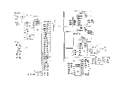
The master control circuit 30 will be described ~n more
detail in connection with Fig. 2, which depicts a functional
block diagram of the master control circuit 30. With
reference to Flg. 2, the master eontrol circuit 30 ha6 ~our
sources of addresses which it may couple over ~ddress lines
31 as MEM ADRS memory address 6iqnals. In particular, the
master control circuit 30 may receive address signals over
data/address lines 15, which address signals are latched in
an address buffer 50 in response to an ADRS LTH addre6s
latch signal from a control circuit 51. The control circuit
51 asserts the ADRS LTH address latch signal in response to
the AS address strobe fiignal. At the same time that the
address buf~er S0 latches the address signals on
data/addres6 lines 15, a latch 83 latches the CYC SEL cycle
select signals which identify a type of operation. The
~30~5 83-447
-29-
latch 83 provides LTH CYC SEL latched cycle select signals,
which are coupled to the control circuit 51.
A second source of address signals is a video address
counter 52, which generates VID ADRS video address signal6
which are used during a video shift register update
operation. A third sources of addresses i8 a refresh
c~
addre~ counter 53'generates REF ADRS refresh address
signals used during refresh op`erations which follow video
shift register update operations. In one specific
embodiment, 6ix refresh operations follow each video shift
regi6ter update operation. In addition, since video shift
regi6ter operation6 in connection with video memory 22 are
performed sufficiently often that refresh of the video
memory 22 ifi not required, refresh operations are only
perormed in connection with the random access memory 20.
Finally, a fourth source of addresses is an interrupt
addresfi circuit S0, which provides an address of an
interrupt vector during an interrupt acknowledge operation
In one embodiment, the memory address lines 31 carry
eight MEM ADRS (7:0~ memory address signals in parallel, and
the data/address lines 15 may carry as many as thirty two
`- ~300755
83-447
-30-
address 6ignals in parallel. The address buffer 50 i6
divided into a low order portion 54 and an intermediate
portion 55, both of which store signals which may be used to
address the memories 20, 21 and 22 during a memory
operation, and a high order portion 56 which latche6 ~ignals
which identify a particular device in the system depicted in
Fig. 1.
~ he contents of the high order portion 56 of the
address buffer 50 are coupled, as DAL DEV SEL data/address
lines device select signals, to a decoder 57. In response
to the DA~ DEV SEL data/address lines device select signals,
the decoder 57 asserts an RAM EN random access memory enable
5c,
signal i the contents of the address buffer ~ identify a
location in random access memory 20.
In addition, the decoder 57 asserts an ROM EN ~ead only
memory enable signal if the contents of the address buffer
identify ~ location in read only memory 21 and a VRAM EN
video m~mory enable slgnal lf the contents of the addres~
buffer 50 identify a location in video memory 22.
Similarly, the decoder 57 asserts a DIS~ EN disk enable or
NET EN network enable signal if the contents of the address
~3Q0~5~
83-447
-31-
buffer 50 identify a location in disk devices 23 or network
interface 24, respectively.
Finally, the decoder 57 asserts an MCC EN master
control circuit enable signal if a control or status
register in the master control circuit 30 is addressed. One
such regi~ter, namely, an offset register 68, i8 depicted in
Fig. 2. The offset register 60 receives a value which is
loaded into the video address counter 52 when the counter
counts out~ The value in the video address counter i6 an
offset into the video memory~s address space used by the
processor 10. The contents of the offset re~ister 60 may be
updated in response to a VID LD video load ~ignal from
control circuit 51 during the monitor's vertical blanking
interval, enabled during ~ervicing by processor 10 of the
vertical blanking interrupt as described above.
The interrupt addre6s circuit ~0 includes an interrupt
ba6e address register 81 which stores the base address of
the interrupt vectors in read only menlory 21 ~Fig. 1) and a
priority encoder 82. The priori~y encoder receives the
interrupt request 61gnals from the devices whlch may request
interrupt service, which signals are identi~ied in Fig. 2 as
INT REQ ~7:0) interrupt request signals (that is, eight INT
~3~7SS
83-447
-32-
REQ interrupt reque~t 6ignals) and generates ~three INT
ADR5 (2:0) interrupt address signals. The register 81
transmits INT BASE interrupt base signals which, in turn,
comprise high order address bits which are used during an
interrupt acknowledge operation. The priority encoder 82
provides INT ADRS t2:0) interrupt address signals which
comprise three low order addrcss bits which are concatenated
onto the INT BASE interrupt base signals to provide INT ACX
ADRS interrupt acknowledge address signals which are used
during an interrupt acknowledge operation to identify the
address of the location in read only memory 21 of the
interrupt vector to be returned.
The content6 of portions 55 and 54 of the address
buffer 50 are transmitted as DA~ ADRS HI data/address lines
addEess high-order portion and DA~ ADRS ~0 data/ad~dress
~ -~?.~ C~. C;\~
llnes addre6s low-order portion signals, ~F-e~pect~ Ly, to
two sets of input terminals of a multiplexer 61. In
addition, the outputs of the video address counter 52 and
refresh address counter 53 are transmitted as VID ADRS video
address and REF ADRS refresh address signals, respectively,
to two other set of input terminals of multiplexer 61. The
INT ACK ADXS interrupt acknowledge address signals are also
~300'75~
. .
83-447
-33-
coupled to a ~et of input terminals of multiplexer 61.
Multiplexer 61 determines, in response to ADRS SEL address
select signals at its ~elect input terminals, the ~ignals to
be coupled onto lines 31 as ME~ ADRS memory address s~gnals.
The multiplexer 61 transmits the signals at the input
terminal identified by the ADRS SEL signals in respon6e to
an asser~ed ADRS OUT EN address out enable signal, which i6
recelved at an output enable terminal from the control
circuit 51. The ADRS SEL address select ~ignal~ are also
provided by control circuit 51.
If the operatlon is a read or write operation, as
defined by the LTH CYC SEL latched cycle select ~ignal from
latch ~3, the control circuit 51 also generates the
appropriate RAM.WE random access memory write enable signal,
V WE video random access memory write enable signal, DISK
WRT disk devices write enable signal, or NET WRT network
interface write ~nable signal, depending on the condition of
the RAM EN random access memory enabling signal, ROM EN read
only memory enabling signal, VRAMIvideo random access memory
enabling ~ignal, DISK EN di6k devices enabling signal, or
NET EN network enabling signal from decoder 57. In
addition, the control circuit 51 generates the DISK AS diSk
address strobe, DISK DS disk data strobe, NET AS network
~3()~755
83-447
-34-
address ~trobe, NET DS network data strobe, RAM R~S and RAM
CAS random access memory row and column address strobe, VRAM
RAS and VRAM C~S video memory row and column address 6trobe
6ignals~ All of these signals are collectively identified
in Fig. 2 as DISK, NET, MEM CTRL SIG disk, network and
memory control signals to enable the operations with those
devices as de~cribed above. Similarly, the control eircuit
51 responds to the various DISK ERR, NET ERR, RAM ERR, ROM
ERR and V~AM ERR error and DIS~ RDY, NET RDY, RAM RDY, ROM
RDY and VRAM RDY ready signals, which are collectively
identified as DISR, NET, MEM RESPONSE SIG disk, networ~ and
memory response signals, and generates the R~Y ready and ERR
error signals in response thereto.
On the other hand, i~ the operation is an interrupt
acknowledge operation, the control circuit 51 generates ADRS
SE~ addres~ select signals which enable the multiplexer 61
to transmit the INT ACK ADRS interrupt acknowledge address
signals as MEM ADRS memory address signals over lines 31.
The con~rol circuit 51 al60 asserts a KOM EN read only
memory enable signal which ls coupled to read only memory 21
to enable it to couple the intereupt vector stored at the
location identified by the INT ACR ADRS interrupt
13007~5
83-447
-35-
acknowledge address signals. At the appropriate time, the
control circuit 51 a~serts the RDY ready or ERR error signal
for transfer to the processor 10.
The master control circuit 30 also includes a video
timer 62 ~hich periodically asserts a VID UPD video update
~ignal to time updating of the video shift register 25. The
VID UPD video update signal is coupled to a synchronizing
flip-flop 63 which synchronizes the VID UPD video update
signal to the SYS CL~ system clock signal. Since a ~OLD
signal is not asserted, an inverter 71 enables one ~nput of
an AND gate 70 to pass the SYS C~K system clock signal rrom
the processor 10 as SYNC CLK synchronizing clock signals to
control two synchronizing 1ip-10ps 63 and 68. On the next
tick of the SYS CLX system clock signal ~that is, when it is
next asserted) after timer 62 asserts the VID UPD video
update signal, 1ip-10p 63 latches the asserted VID VPD
video update signal from timer 62 and generates an asserted
VID VPD SYNC video update synchronized si~nal. The asserted
VID UPD SYNC video update synchroni~ed signal enables one
input of an AND gate 64.
If the ~S address strobe signal is in the asserted
condition, indicating that a previously enabled operation is
~3007SS
B3-447
-36-
in progress, an inverter 65 disables one input of an AND
gate 66. Since the HOLD signal is negated, an ~nverter 67
enable6 the 6econd input of the AND gate 66. When the AS
address 6trobe ~ignal is negated at the end of the
previously enabled operation, inverter 65 enables the second
input of AND gate 66, which, in turn, energize; the AN~ gate
66. Thi~, in turn, enables the second input of AND gate 64,
thereby energizing it.
The energized AND gate 64 enables the data input
terminal of flip-flop 68. At the next tick of the SYS CL~
system clock signal, the flip-flop is set, which a~serts the
HOLD signal.
The HOLD signal i6 coupled to control circuit 51. When
the HO~D signal i5 as6ert~d, the control circuit ls enabled
to generate the slgnal6 described above to perorm the video
~hit ~egi6ter update operation, followad by the refresh
operations. In particular, the control circuit 51 initially
generates ~DRS SEL address select 6ignals and a~serts the
ADRS OUT EN address out enable signal to enable the video
addres~ counter 52 to couple the VID ADRS video addres6
signals from the video address counter 52 onto lines 31 as
the MeM ADRS memory address 6ignals. A relectcd time later,
.
)755
83-447
-37-
after the MEM ADRS memory address ~ignals have had a chance
to settle, the control circult 51 asserts the VRAS video row
address strobe ~ignal.
A selected time later the control circuit 51 enables
the multiplexer 61 to transmit MEM ADRS memory address
6ignals of all zeros by negating the ADRS OUT EN address out
enable signal. A selected time later, after these MEM ADRS
memory address signals have sét~led, the control circuit 51
asserts the VCAS video column address strobe signal. In
response, the video memory 22 transmits VID OUT signals
sufficient to ill video shift register 25, and the control
circuit 51 asserts the VSR LD video shi~t register load
fiignal to enable the video shift register 25 to load the VID
OUT signal6~ The control circuit 51 then negates the VRAS
and VCAS video row and column address strobe signals and
asserts a VID INCR video increment signal which enables the
video addre6s counter 52 to increment.
; Ther~fter, the control circuit Sl enables a succe6sion
of rereah operations to occur in random access memory 20.
In particular, the control circuit 51 generates ~DRS SEL
address select signals and asserts the ADRS OUT EN address
out enable signal which enable the multiplexer 61 to couple
~L3~)~75~5
~ 66822-62
the REF ADRS refresh address signals from re~resh ~ddress
counter 53 on~o lines 31 as the MEM A~RS memory address
signals. A selected time later, after ~he MEM ADRS memory
address signals have settled, the control circuit 51 asserts
the RAM RAS random access memory row address strobe signal to
enable the iden~ified row of storage locations in the random
access memory 20 to be refreshed. The control circuit 51 then
negates the RAM RAS random access memory row address strobe
signal to terminate the refresh opera~ion and asserts a REF
INCR refresh increment signal which enables the refresh address
counter 53 to increment. This process is repeated a selected
number of times to allow multiple rows in random access memory
20 to be refreshed.
During thls time, the HOLD signal remains asserted.
While the HOLD siynal is asserted, inverter 67 disables AND
gate 66 so that a change in the conditlon oi the AS address
skrobe siynal does not affect the aondition of AND gate 64.
The asserted H01,D signal disables AND gate 70 to isolate the
flip-flops 63 and 68 from the SYS CLK system clock signal.
Thus, after the HOLn slgnal is asserted, the successive ticks
of the SYS CLK system clock signal by the processor 10 do not
affect the respective condi~ions of the flip-flops 63
~3~)7~iS
83-447
-39-
and 68. ~t the end of the refresh operations, the control
circuit 51 asserts a VID RST video reset signal which causes
video timer 52 and flip flops 63 and 68 to re~et.
As described above, She processor 10, disk devices 23
; or network interface 24 may attempt to initiate a transfer
while a video shift register update operation or refresh
operation is in progress, and, as part of that transfex, the
AS address strobe slgnal is asserted; In response to the
assertion of the AS address strobe signal, the control
circuit S1 ensures that the RDY ready signal is at a negated
level. In addition, the control circuit 51 asserts the ADRS
LTH address latch signal which enables the address buffer 50
to latch the address signals on the data/address lines 15.
Furthermore, the control circuit S1 asserts an EN PH
CTR enable phase counter signal which is coupled to a phase
counter 72. The asserted EN PH CTR enable phase counter
signal enablefi the phase counter 72 to load and thereafter.
increment in response to the successive SYS CLK system clock
6ignals from processor 10. The control circuit 51 uses the
phase counter 72 to synchronize restarting of the transfer
operation following termination of the video shift register
update operation and reiresh operations, so as to ensure
:
` , .
~ 3~ 5~
33-447
-40-
that the memory operation initiated by, ~or example, the
processor 10, i5 restarted in synchronism with the same
clock phase of processor 10 during which the processor 10
began the tra~s~er operation.
That i5, if processor 10 initiates a transfer operation
in synchronism with phase 2 of a four phase clock, the
eontrol circuit restart~ the transfer operation, after the
video shift register update operation and refresh
operations, in synchronism with phase 2. The control
circuit 51 does not, however, receive a signal corresponding
to the processor~s clock phases, and so it uses phase
counter 72 to count clock phases in response to t~e SYS CLK
syst0m clock signal, which is ticked to identify th~ ticks
o the processor' 5 6uccessive clock phases. When the phase
o~ \
counter 72 counts out, it asserts a P~ASE CTR -T-~ phase
counter time out signal which is coupled to control circuit
51. If the control circuit has not performed all of the
successive refresh operations, it again asserts the EN PH
CTR enable phase counter signal to enable the phase counter
72 to reload. On the other hand, if the control circuit 51
has enabled the last refresh operat~on, when the phase
~ o~-~'
counter assert~ the PHASE C~R -~ phase counter time out
~3~07~S B3-447
-41-
~ignal, the control circuit 51 then initiates the transfer
operation previously enabled by the processor 10, disk
devices 23 or network interface 24, using the address
latched in the address buffer 50, as described above.
The ~ystem depicted in the Figs. ensures that the video
data will be transferred from the video memory 22 to the
video shift register 25 expeditiously on the timing out of
the vidao timer 62, even though other units in the system
may wish to access one or more of the memories, including
the video memory 22. The master control circuit ensures
that this transfer can take place, even while other units
may wish to perform a transfer to or from the memory. The
processor 10, on the other hand performs arbitration,
allowing only one unit to attempt to access a memory at a
time to perform a direct memory access operation.
In addition, the system simplifies interrupt
processing. In particular, the system enables a number of
interrupt request 6ignals to ba accumulated and coupled to
the proce6sor as a single interrupt request signal. In
addition, if a number of units are requesting interrupts,
the master control circuit may select one of them according
to some order of priority. Further, the system facilitates
. .
. .
~3~7S~
66822-62
simplification of the various units which can be connected into
it, as the units do not have to have the interface circuitry to
respond to the interrupt acknowledge operations or transfer
their interrupt vectors. Finally, the system simplifies
changing the interrupt vectors, since they are all located in a
single unit, namely, the read only memory 21.
The foregoing description has heer. limited to a
specific embodiment of this invention. It will be apparent,
however, that variations and modifications may be made to the
invention, with the attainment of some or all of the advantages
of the invention. Therefore, lt is the object of the appended
claims to cover all such var:Lations and modificatlons as come
wlthin the true splrit and scope of the lnvention.
42
~.7