Note: Descriptions are shown in the official language in which they were submitted.
~3~076~ ~
Description
SEMICONDUCTOR DEVICES HAVING CLOSELY SPACED
DEVICE REGIONS FORMED USING A SELF ALIGNING
REVERSE IMAGE FABRICATION PROCESS
The present invention relates generally to
semiconductor devices and methods of fabricating the
same, and more particularly to a self-aligned method
for fabricating semicond1ctor devices using a reverse
image process.
.
Back~round of the Invention
Major efforts in the development of integrated
circuit semiconductor devices have been directed
towards decreasing the size and spacing of the devices
and towards efficiently fabricating different ~amilies
Of devices on the same semiconductor chip. Extensive
effort~, for example, have been directed towards the
manufacture of BICMOS logic which includes both
bipolar and complementary metal-oxide semiconductor
devices on the same semiconductor chip. For such
BIC~OS logic to be successful, it must be capable of
efficient manu~acture, i.e. not re~uire too many
complex or expensive processing steps. Further, the
finished logic circuit must provide small, densely
packed, high performance devices.
One method of manufacturing semiconductor devices
to provide smaller device size and decreased device
spacing is that known as "lost wax" or "reverse image"
processing. In such processes, a protective structure
~` such as a stud or ridge is formed on a silicon wafer.
Doping and/or various other process are performed
using the protective structure as a mask. The
structure is subsequently removed in the final steps
of the process. Examples of such a method include:
U.S. Pat. No. 4,571,817 to Birritella et al.; and J.
~5
FI9-87-029 -1~
~! 1300764
Jiyamoto et al. "A 1.0 Micron N-Well CMOS/Bipolar
Technology for VLSI Circuits", IEDM 1983, pgs 63-66.
The following are of interest as directed towards
the manufacture of BICMOS devices: U.S. Pat. No.
4,299,024 to Piotrowski; U.S. Pat. No. 4,475,279 to
Gahle; U.S. Pat. No. 4,507,847 to Sullivan; U.S. Pat.
No. 4,484,388 to Iwasaki; U.S. Pat. No. 4,637,125 to
Iwasaki et al.; U.S. Pat. No. 4,486,942 to Hirao; F.
Walczyk, J. Rubinstein, "A Merged CMOS/Bipolar VLSI
10 Process", IEDM 1983, pgs. 59-62; ~. Higuchi et al.,
"Performance and Structures of Scaled-Down Bipolar
Devices Merged with CMOSFETS", IEnM 1984, pgs.
684-687.
U.S. Pat. No. 4,419,809 to Riseman et al.,
15 assigned to the assianee of the present invention,
uses the above-described "lost wax" method to form the
; drain region of a MOSFET~ Riseman et al. further
shows the use o~ sidewall technology to form a
sub-micron device channel.
U.S. Pat. No. 4,5~8,579 to Goth et al., assigned
to the assignee o~ the pre~sent invention, shows a
method of formillg lateral device structures using
însulating studs formed rom oxide sidewalls.
U.S. Pat. No. 4,160,991 to Anantha et al.,
25 assigned to the assignee of the present invention
shows a method of forming high performance hipolar
transistors having closely spaced base-emitter
contacts.
In summary, a process which yields semiconductor
30 devices having smaller or more closely spaced device
regions provides a substantial c~ntribution to the
art; Such a process is of even greater value if it
can be economically and efficiently implemented,
particularly with different device types.
Summarv of the Invention
The principal object of the present invention is
to provide a new and improved method of fabricating
FI9-87-029 -2-
01)~6a~
semiconductor devices.
Another object of the present invention is to
provide such a method capable of fabricating small,
densely packed semiconductor devices.
A further object of the present invention is to
provide such a method which is economically and
efficiently applicable to the fabrication of bipolar,
insulated gate, and BICM~S logic devices.
Yet another object of the present invention is to
provide new and improved semiconductor devices having
small, densely packed device regions.
In accordance with the present invention, there
is provided a new and improved method of forming a
semiconductor device on a body of semiconductor
material having a first doped region of a first
conductivity type, comprising the steps of: forming a
stud over the first doped region; using the stud as a
mask to form a second doped region of a second
conductivity type in the surface of the first doped
region adjoining the stud; forming a sidewall ~f
insulating material on the stud; forming a first
device contact within the sidewall; and forming a
second device contact over the second doped region
adjoining the sidewall, such that the first and second
contacts are separated by the sidewall.
In accordance with an embodiment of the present
invention, the step of forming the second device
contact includes the step~ of forming a layer of
conductive material genera~ly conformallv over the
first doped region, the stud, and the sidewall, and
then planarizing the layer of conductive material to a
height equal to or less than that of the sidewall.
The second contact is thus self-aligned with the first
and second doped regions and the first device contact.
The method of the present invention can
beneficially be utilized to fabricate new and improved
bipolar transistors, insulated gate tran5istors, and
BICMOS logic including both types of transistors. It
FI9-87-029 -3-
130~)76~
can further be used to fabricate any other type of
semiconductor device which utilizes the self-aligned,
closely spaced device regions and contacts of the
present invention.
:
Brief Description of the Figures
These and other objects, features, and advantages
of the present invention will ~ecome apparent to the
reader from a consideration of the following detailed
description of the invention when read in conjunction
with the drawing Figures, in which: -
Figs. 1-19 comprise sectional views illustrating
successive process steps in constructing a BICMOS
semiconductor device in accordance with the present
invention, with Figs. llA and 14A comprisinq top views
of the imm~diately preceding sectional view.
Detailed Description of the Invention
The following cletailed description of the
invention is di~ected to a process of fabricating a
BICMOS devlce including a pair of N- and P- channel
enhancement mode CMOS devices and an NPN bipolar
transistor. It will be understood that the particular
conductivity types and concentrations described herein
are exemplary in nature. Through the reversal of
conductivity types and/or the appropriate adjustment
of conductivity concentrations, it will be apparent to
those skilled in the art that the present invention
can be used to fabricate CMOS devices of differing
concentrations and/or a ~NP-type bipolar transistor.
It will also be understood that the present invention
is not limited to the fabrication of BICMOS devices,
but has utility in the fabrication of separate bipolar -
and insulated gate devices, as well as in the
fabrication of other types of semiconductor devices
; requiring closely spaced, highly aliqned device
~ 35 regions.
! Referrinq now to Fig. 1, a wafer or substrate 10
FI9-~7-029 -4-
. . .
~3~7~4
of P- silicon monocrystalline material is provided,
preferably having a <100~ crystallographic orientation
and a resistivity in the range of 10-20
ohms~centimeter. An N+ subcollector region 12 is
formed in substrate 10, for example by a conventional
process of implanting arsenic (As) ions to a concen-
tration in the range of about lxlOl9-lx102 atoms/cm3.
Altè~natively, N~ subcollector region 12 can be formed
by conventional diffusion processes.
Referring now to Fig. 2, a P- epitaxial layer 14
is grown on layer 12, for example using a conventional
low temperature, low pressure silicon epitaxial
process. Layer 14 is preferably formed to a thickness
in the range of about 0.6-1.5 microns.
Examining now Fig. 3, a pair of N well regions
14A, 14C are formed in layer 14 so as to bound an
undistl~rbed P- well region 14B. Regions 14A and 14C
' are formec, for ex~mple, by the selective implantation
o arsenic or phosphorous ~P) ions into layer 1~ using
stand~rd photolithographic maskiny processes to block
out region l~B. Regions 14A, 14C can be completed
; using conventional dopant drive-in processes.
Re~exring now to Fig. 4, four deep isolation
regions 16, 18, 20, 22 are formed at the lateral
25 boundaries of wells 14A, 14B, 14C. In the present
embodiment, each deep isolation region 16, 18, 20, 22
is generally T-shaped, including a deep trench
(T-base) extending vertically downward through layer
12, and a:shallow T-cap at the surface of the device
extending partway into the adjoining wells. Adjacent
deep isolation regions 16, 18 are used to electrically
isolate a transistor device subsequently formed in
well 14A. Similarly, adjacent deep isolation regions
18, 20 and 20, 22 are used to electrically isolate
transistor devices subsequently formed in wells 14B
and 14C, respectively. A shallow isolation region 24
is formed at the surface of well 14C, spaced laterally
from the T-cap of isolation region 20 to electrically
FI9-87-029 ~5~
~1.3~076~
isolate subsequently formed elements of a bipolar
transistor. Isolation region 24 is spaced, for
example, a distance Dl in the range of about 1-10
microns from the cap of deep isolation region 20, and
extends down into well 14C.
Shallow isolation region 24, as well as the
T-caps of deep isolation regions 16, 18, 20, 22, can
be formed, for example, using conventional recessed
oxide isolation ~ROI) or shallow trench isolation
processes. Subsequent to the formation of the T-caps
of deep isolation regions 16, 18, 20, 22, the deep
trenches are formed, for example, by conventional SiO2
or polysilicon filled deep trench isolation methods.
The above-described methods of forming shallow and
deep isolation regions are well known to those skilled
in the art, and may be reversed as desired to form the
deep trench regions first.
Referring now to Fig. 5, an N~ subcollector
reachthrough region 28 is formed between isolation
regions 20, 24 extending downward from the upper
surface of w~ll 14C into subcollector layer 12.
Region 28 is formed, for example, by a conventional
process of diffusing POC13 into well 14C between
isolation regions 20, 24. This difusion process is
followed by a conventional oxidation process such as
thermal o~idation in a wet oxygen ambient. This
diffusion process drives the phosphorous dopant
downward to complete subcollector reachthrough region
28, and forms an oxide layer 34 on the surface of the
device. Oxide layer 34 is formed, for example, to a
thickness of about 100-500 Angstroms, the layer being
appreciably thicker a~ the surface of subcollector
reachthrough region 28.
Referring still to FigO 5 ~ the surface conduc-
~5 tivi~ies of wells 14A, 14B are adjusted where MOStransistors are to be formed, so as to provide desired
threshold voltages VT for these transistors. For the
P-channel MOSFET to be formed in well 14A, for
FI9-87-029 -6-
"` ~L300~6~
example, depending on whether the transistor is
desired to operate in an enhancement or depletion
mode, boron or phosphorous ions, or both, are selec-
tively implanted shallowly into the surface of the
well.to form a region 30 with a dosage in the range of
about l-10xl012/cm2. For the N~channel MOSFET to be
formed in well 14B, for example, boron ions are
selë~tively implanted shallowly into the surface of
the well to a dosage in the range of about
10 1-5xlO12/cm2,
Referring now to Fig. 6, a layer 36 of conductive
material is formed over layer 34. For the purposes of
the present invention, suitable conductive materials
for layer 36 include high-temperature,
high-conduc~ivity conductors such as conductive
polysilicon, polycide ~comprising polysilicon with a
metal silicide coating), and refractory metals such as
tungsten silicide (WSi2). In a preerred embodiment
of the invention, layer 36 comprises an intrinsic
~non-doped) polycrystalline silicon ~polysilicon)
~ormed by a conventional chemical vapor deposition
~CVD) process to a thickness in the range o~ about
2,000-6,000 An~skroms.
Subsequent to the formation of layer 36, regions
2S 37A, 37C of the layer, overlying wells 14A, 14C/
respectively, are doped to N+ concentrations using
conventional, selective As or P ion implantation.
Similarly, a region 37B of layer 36, overlying well
14B, is doped to P~ using conventional, selective
boron ion implantation. Alternatively, if it is
desired to simplify the fabrication process,
polys-licon layer 36 can be formed in situ doped to an
N+ concentration in the range of not less than 2x10²
atoms/cm3.
.Subsequent to the formation of layer 36, an
optional layer 38 of silicon dioxide can be formed
thereon by a conventional CVD process. When used,
layer 38 is preferably formed to a thickness of about
FI9-87-029 -7~
~3~0764
100-500 Angstroms, and functions to facilitate the
delineation of the studs described below, and to
relieve interlayer stresses between layer 36 and a
subsequently formed nitride layer 40. Nitride layer
40 is formed, for example, by a conventional CVD
process to a thickness in the range of about
1,000-2,000 Angstroms.
~Subsequent to the formation of layers 34, 36, 38,
40, a conventional photolithographic process is used
to form resist mask regions 42, 44, 46. Mask regions
42, 44 are centered over regions in wells 14A, 14B,
respectively, which will subsequently form the gates
of completed CMOS transistors. Mask region 46 is
centered over the surface of well 14C (i.e. the
l; surface between the edges of isolation regions 22,
24), a region which will subsequently form the emitter
of a completed bipolar transistor.
Referring now to ~ig. 7, the portions of layers
36, 38, and 40 not covered by resist mask regions 42,
44, 46 ar~ removed via appropriate reactive ion
etching processes, i.e~ processes having good selec-
tivity and anisokropy, to expose underlying oxide
layer 34~ Appropriate RIE etchants include: CF4+O2 to
remove silicon nitride layer 40; CF~+H2 to remove
silicon dioxide layer 38; and C12+~r or CF4+O2 to
remove polysilicon layer 36. The resist mask regions
42, A4, 46 are then stripped with an oxide plasma to
delineate studs 48, 50, 52 over wells 14A, 14B, 14C,
respectively. With the doping of layer 36 performed
as described above, the portions of the layer remain-
ing in studs 48, 50, 52 are doped to N+, P+, N+,
respectively. If layer 36 had been formed in situ
doped N+ in accordance with the alternate embodiment
described above, these same portions would be doped to
N+.
Referring now to Fig. 8, oxide layer 34 outside
the regions of studs 48, 50, 52 is removed, for
example through the use of a carbon tetraflouride
FI9-87-029 -8-
~ ~30~764
(CF4) plasma etch or a diluted, buffered hydroflouric
acid etch. Because layer 38 was thicker at the
surface of subcollector reachthrough 28 than over the
remainder of the device surface, a protective portion
60 of the oxide remains after the above-described
etch. Subsequent to the removal of layer 34, a
photolithographic blocking mask 61 is formed over the
surfa`ce of the device between isolation regions 18 and
24 so`as to mask the surface of well 14B. A conven-
tional, blanket boron ion implantation is then per-
formed with a dose in the range of 1x10¹² atoms/cm3 to
; lxln13 atoms/cm3. This boron ion implantation con-
verts the surface region of well 14A not underneath
stud 48 'nto P type lightly doped drain (LDD) regions
54A, 54B, and the surface region of well 14C not
underneath stud 52 into P type intrinsic/extrinsic
base link-up region 58.
As shown in Fig. 9, a pair o ~2hotolithographic
blocking masks 63, 65 are formed over wells 14A, 14C,
respectively. Subsequently, a conventional, blanket
arsenic ion implantation is performed with a dose in
the range o~ 1-lOxlO13atoms/cm2. This implantation
converts the surface region o well 1~B not underneath
stud 50 into N type LDD regions 56A, 56B. The result-
ing device with the photolithographic masks removed isshown in Fig. 10.
Referrin~ now to Fig. 11, subsequent to the
completion of the various ion implantations to form
the above-described LDD and link-up regions~ silicon
dioxide sidewalls 62 are formed on the sides of each
of studs 48, 50, 52. For purposes of explanation, the
sidewall 62 formed on stud 48 is designated with the
suffix A, the sidewall formed on stud 50 is designated
with the suffix C, and the sidewall formed about stud
52 is indicated with the suffix E. From a considera-
tion of the top view in Fig. llA, it will be appreci-
ated that studs 48, 50 completely bisect what will be
the active regions of the subsequently formed CMOS
FI9-87-029 ~9~
~3~7~;4
transistors. Thus, LDD regions 54A, 54B, 56A, 56B
comprise electrically separate regions spaced by the
studs 48, 50, respectively. Stud 52, however, is
situated with its sidewall 62E entirely withln what
will be the active region of the subsequently formed
bipolar transistor. Link-up region 58 thus comprises
a uhitary electrical region surrounding stud 58.
Sidewalls 62 are formed, for example, by first
using a conventional CVD process to form a conformal
layer of SiO2 (not shown) to a thickness in the range
of about 1,000-5,000 Angstroms. Subsequent to the
formation of this conformal layer of SiO2, an
anisotropic RIE etchant such as CF4 + 2 is used to
re~ove the horizontal portions of the layer, leaving
vertical sidewalls 62.
Referring now to Fig. 12, a layer 64 of polycide
with accompanying metal silicide surface 64A is
~eposited conformally over the top of the device to a
thickness D2 of at least the vertical height of
sidewalls 62, or since the sidewalls cover the ver-
tical sur~aces o~ studs 48, 50, 52, the height of the
studs. Layer 64 is ~ormed, for example, by a conven-
tional low pressure CVD process.
Subse~uent to the formation of layer 64, the
layer is planarized evenly with the tops of sidewalls
62 and studs 48, 50, 52 to ~orm the device shown in
Fig. 13. This planarization is accomplished, for
example, by the use of a photoresist reflow and RIE
etch-back:process or by a chemical-mechanical
(chem-mech) polish. An acceptable chemical-mechanical
polish process is shown in U.S. Patent No. 3,911,562
to Youmans.
An exemplary photoresist reflow and RIE etch-back
~; process is shown in the article "A Practical Trench
Isolation Technology with a Novel Planarization
Process", to Fuse et al., IEDM 1987, pgs. 732-734.
~riefiv, the~article~~~~ scribes a nrocess whereln ~ `~
` lar~;e valleys in~ ~ ~~
FI9-87-029 -10-
007~4
the SiO2 are filled with a first photoresist. A thin
layer of SiO2 is sputtered over the entire device, and
a planarizing layer of second photoresist deposited
over the sputtered SiO2. The second photoresist is
etched to the surface of the sputter-deposited SiO2.
The sputter-deposited SiO2, resist films, and underly-
ing SiO2 are subsequently etched to the desired height
with a gas of CHF3, C2F6, and 2
After the planarization of layer 64, regions 64B
of layer 64 surrounding stud 50 are selectively doped
with arsenic (As), while regions 64C of layer 64
surrounding studs 48 and 52 are selectively doped with
boron. Both regions 64B and 64C are doped to a
concentration in the range of about l-lOx102
atoms/cm3. Both of these dopings are performed using
conventional ion implantation processes with conven-
tional photolithographic masking.
Referring now to Figs. 14, 14A ".ayer 64 is
delineated to orm five discrete regions which, for
purposes o~ explanation, are indicated by reference
numbers 66A, 66B, 68A, 68B, and 70, region 70 forming
a rectangular ring about stud 52 and sidewall 62E.
Regions 66A, 66B adjoin opposite sidewalls of stud 48,
the former overlying LDD implant region 54A and the
latter extending from the edge of isolation trench 18
to overlie LDD implant region 54B. Regions 68A, 68B
adjoin opposite sidewalls of stud 50, with the former
extending from an edge of isolation trench 18 to
overlie ~DD implant region 56A, and the latter extend-
ing from an edge of isolation region 20 to overlie LDDimplant region 56B. Region 70 forms a ring about the
sidewalls of stud 52, with the left half (as viewed in
the Figs.) extending from an edge of isolation trench
24 to overlie intrinsic-extrinsic base link-up region
58, and the right half extending from an edge of
isolation trench 22 to overlie the other side of the
link-up region.
FI9-87-029 -11-
~--' gL311~07~;4
The delineation of layer 64 to form regions 66,
68, and 70 as shown in Fig. 14 is accomplished, for
example, by the use of an appropriate RIE etchant such
as CF4 + H2 in combination with conventional
photolithographic masking.
Referring now to Fig. 15, subsequent to the
delineation of regions 66A, 66B, 68A, 68B, and 70, the
device is subjected to thermal oxidation so as to form
a layer 72 of SiO2 over the exposed surfaces of these
regions to a thickness in the range of about
1,000-5,000 Angstroms. Layer 72 is not formed, of
course, over the exposed surfaces of the device or
over the tops of studs 48, 50, 52 which are protected
by the nitride. This last-described process of
thermal oxidation further operates on che device of
Fig. 1 to drive impurities from regions 66A, 66B, 68A~
68B, and 70 downward into the device, deepening and
completing the ~ormation of the source, drain regions
54A, 54B, the source, drain regions 56A, 56B, and the
extrinsic base region 58.
ReEerring now to Fig. 16, stud 52 over well 14C
is removed to leav~ sidewall 62E bounding an exposed
area on the well surface. Stud 52 is removed by first
etching nitride layer 40 with a CF4/O2 plasma etch or
a hot bath of phosphoric acid (H3Po4)~ The relatively
thin layer 38 of silicon dio~ide is removed by dipping
in BHF without substantially disturbing the much
thicker layer 72 and sidewall 62E of silicon dioxide.
Polysilicon layer 36 is removed, for example, with a
pyrocathecal etch, and silicon dioxide layer 34 is
removed with BHF. It will be appreciated that the
step of removing silicon dioxide layer 34 with a B~F
dip etch can be carefully controlled to stop at the
surface of well 14C so as not to etch into the device
surface or otherwise disturb the nature of the subse-
quently formed bipolar transistor.
~ Subsequent to the removal of stud 52, a buried
,~ subcollector implant region 74 is formed in well 14C
FI9-87-029 -12-
` ~306)764
by a conventional implantation of arsenic or phos-
phorus ions. Because the remainder of the device is
masked by polysilicon regions 66A, 66B, 68A, 68C, 70,
overlying layer 72, and studs 48, 50, this implanta-
tion is effective only in the window opened withinsidewall 62E by the removal of stud 52. The surface
of subcollector reachthrough 28 is exposed to the
implantation. However, the dopant concentration of
subcollector reachthrough region 28 is sufficiently
larger than that of subcollector region 74 so it is
not appreciably altered.
Following the formation of buri.ed subcollector
region 74, a conventional, b;anket implantation of
Boron ions is performed with a dose in t~e range of
l-lOx1012 atoms/cm2 to form an intrinsic base region
75.
After the ormation of intrinsic base region 75,
a conventional, blanket implantation of A~senic ions
is performed with a dose in the xange of l-lOx1015
atoms/cm to orm an emitter region 76. Alterna-
tively, emitte~ region 76 can be out-diffused from the
emitter polysilicon deposited as described
hereinbelow, or from a combination of both of these
processes, It will be understood that buried region
74, intrinsic base region 75, and emitter region 76
can be formed in interchangeable order.
In each of the above-described implantation
steps, the polysilicon regions 66A, 66B, 68A, 68C, 70,
overlying layer 72, and studs 48, 50 function as
implant blocking masks, in the manner described above,
to block the Boron and Arsenic ions from entering the
underlying device regions. Also in the manner
described above, the dopant concentration of
subcollector reachthrough region 28 is sufficiently
high..that it is left effectively undisturbed.
Referring now to Fig. 17, a layer 80 of ln situ
arsenic doped polysilicon, having a concentration in
the range of about l-lOx102 atoms/cm3, is formed over
FI9-87-029 -13-
L30076~
the exposed inner surface of sidewall 62E and overly-
ing emitter region 76. Subsequent to the formation of
layer 80, a layer 82 of metal silicide is formed
thereover in the manner shown in Fig. 18 to increase
the conductivity o~ layer 80. Alternately, layer 80
can comprise an intrinsic polysilicon later doped by a
; conventional implantation with arsenic ions to a
concentration in the range of about l-lOx102
atomslcm3. Layer 80 is formed, for example, by a low
pressure CVD process. Layer 82 is formed, for
example, by physically evaporating or sputtering a
thin layer of metal, for exam~le titanium, over layer
80, and converting it into a metal silicide using an
alloy si.nteriny anneal. If it is cesired to form
emitter region 75 ~rom, or increase the concen~ration
of the emitter region by out-diffusion from layer 80,
then an emitter dopant drive-in anneal, in a tempera-
ture range of about 800-950 degrees centigrade, is
performed prior to the formation of layer 82.
~; 20 Continuing to describe Fig. 18, the nitride cap
layers 40 on the tops oE studs 48, 50 are remove with
a phosphoric acid etch ~H3PO4) to leave thusly altered
studs 48', 50', respectively.
Referring now to Fig. 19, conventional processes
2S are used to form contact holes 84, 86, 88, 90, and 92
through layer 72 to expose surface areas of
polysilicon regions 66A, 66B, 68A, 68B, and 70,
respectively. Conventional processes are again used
to form metal interconnections 94, 96, 98, 100, 102,
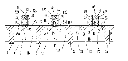
30 104, 106, 108, and 110. Metal contacts 94, 98, 100,
104, and 110 are disposed in contact holes 84, 86, 88,
90, and 92, respectively. Metal contacts 96 and 102
overlie polysilicon layer 38 in studs 48', 50',
respectively. Metal contact 106 spans isolation
regions 20, 24 so as to overlie subcollector
reachthrough region 28, and metal contact 108 overlies
polycide layer 82 over well 14C. Each of the metal
FI9-87-029 -14-
3~
interconnections described above makes ohmic elec-
trical contact with the underlying, contacted region.
In accordance with the above-described embodiment
of the invention, there has thus been formed an
N-channel MOSFET in the region of isolated device well
14A, a P-channel MOSFET in the region of isolated
device well 14B, and a vertically disposed NPN bipolar
transistor in the region of isolated device well 14C.
Metal contacts 96, 98, and 94 form the gate, drain and
so~lrce of the first MOSFET, respectively. Metal
contacts 102, 10~, and 100 form the gate, drain, and
source contacts of the second MOS~ET, respectively,
and metal contacts 108, 110, ana 106 form the emitter,
base, and collector of the bipolar transistor, respec-
tively. The thusly formed BIC~50S logic is fabricated
with a cost~effective number of process steps. Inaccordance with one major feature o~ the present
invention, the use of studs 48, 50, S~ to act as masks
or the various device regions, in combination with
khe forming and delineation o~ polysilicon layer 64 to
form device contact regions 66A, 66B, 68A, 6~, and
70A, 70B, results in self-aligned, electrically
conductive contacts for the CMOS and bipolar transis-
tors. These self-aligned features, formed in accor-
dance with the reverse image process of the present
invention, provide improvement in process control andfabrication reproducibility. They further provide
significant increases in the speed and the reliability
of the resulting transistors. In accordance with
another major feature of the present invention, the
use of the silicon dioxide sidewalls 62 in the manner
described above provides very close spacing, i.e. on
the order of 0.1-0.5 microns, between the base and
emitter contacts of the NPN transistor and between the
gate and source/drain contacts of the CMOS transis-
tors. This provides the significant advantages of
decreased size, increased density, and significantly
increased speed of the integrated circuits. It will
FI9-87-029 -15-
' ~ ~3t:)~7~i~
be appreciated that device contact regions 66A, 66B,
68A, 68B function as extrinsic drain/source regions,
and device contact regions 70A, 70B function as
extrinsic base regions.
There is thus provided a BICMOS logic circuit and
a method o~ forming the same. The circuit includes
densely packed, high-speed devices formed by a com-
bination of reverse image and self-aligned process
steps. The process used to form the BICMOS logic
circuit is readily adaptable to the formation of other
types of logic circuits, including exclusive bipolar
or CMOS devices, and other semiconductor devices which
can benefit from the se]f-alignment techniques of the
present invention. The process has particular indus-
lS trial application in the rormation of highly inte-
grated logic circuits.
While the present invention has been shown and
described with respect to part cular embodiments,
numerous changes, modiFications, and improvements will
occur to those skilled in the art without departing
rom the scope and spirit of the invention.
, .
~I9-87-029 -16-