Note: Descriptions are shown in the official language in which they were submitted.
13V1~73
BACKGROUND AND SUMMA~Y OF THE INVENTION
The present invention relates generally to an apparatus and
method for measuring power and power losses of liyht ~ransmissions
in fiber optic cables, and more specifically, the power and power
losses resulting from the transmissions of known wavelengths of
light. ~
Fiber optic cables have been finding increased applications in
a variety of industries as a result of their iightweight
composition and effectiveness in transferring information. T~e
use of fiber optic cables has, for instance, become common in the
telecommunications indust`ry, where many of the bulkier and less
efficient wire data lines are being replaced with fiber optic
cables. To assure accuracy of the data transmitted by light
signals, however, these fiber optic cables are tested by measuring
the power losses associated with the light transmissions, and
thus, determine the potential error in the data transmissions.
Light signals constituting data transmissions are transmitted
throug'n fiber optic cables using specific nominal wavelengtns of
light for the transmission. Because differen~ wavelengths of
light have varying attenuating characteristics, it is important to
determine the attenuation of the fiber optic cable with respect to
the specific wavelength of light which will be used for the
particular data transmiSSiGn.
- 2 -
.~ , ~ . ~
-
13~1~73
In U.S. Patent 4,234,253 to Higginbotham et al., an
attenuation measuring system is described as having a transmitter
and receiver which are operativeiy connected to opposite ends of a
fiber optic cable under test. A reference signal comprised of a
timing pulse is superimposed upon a square wave pulse. This
modified square wave~signal is then transmitted through the fiber
optic cable where it is detected by a receiver attached to a
second end of the cable. ~he receiver separates the timing pulse
from the transmitted pulse for use in demodulating the transmitted
signal and compares the demodulated square wave signal to a
reference signal contained within the receiver. The use of a
.
modified square wave pulsë as a test signal, however, has the
disadvantages of signal noise and limited ~andwidth which are
characteristic of DC signals.
U.S. Patent 4,280,765 to Pophillat et al. describes a
measuring system for measuring the transmission bandwidth of the
fiber optic cable using a plurality of sinusoidal test signals as
opposed to square wave pulses. Pophillat, therefore, avoids some
of the disadvantages of Higginbotham. This system comprises a
frequency generator for producing a first composite signal having
discrete distribution of predetermined sinusoidal frequencies. A
single laser is provided by which the first composite signal
modulates the light signal for transmission through the optical
fiber under test. An optical detector is positioned at a
receiving end for converting the light signal into a second
` . ,
13~)1473
-- 4 --
composite signal and directing the same to a spectrum
analyzer. The analyzer provides a frequency spectrum display
of the composite of the electrical sinusoidal signals which
is compared with the spectrum of the first signal for
determining the power attenuation of the first composite of
signal transmissions. While the prior art has concentrated
on techniques of measuring the response to the specific
wavelength of light that is being transmitted, they have
failed to address the problem of providing a tester which is
capable of being adapted for the varying numbers of
wavelengths which may be used. As more and more different
sources of light become available, and the quality af light
fibers increases, a single tester at a single wavelength will
not be sufficient.
It is, therefore, an object of the present disclosure to
provide a means for determining the power losses associated
with any specific wavelengths of light transmissions.
Another object of the present disclosure is to provide a
means for identifying the wavelength of light signals
transmitted through a fiber optic cable under test and for
determining the power losses associated with the respective
light wavelengths.
Yet another object is to provide a means for determining
the power losses associated with specific wavelengths of
light transmissions, using either a laser or an LED as a
source for the light transmissions.
13(;~73
-- 5 --
Still another ob~ect is to provide a means for measuring
the optical power transmitted through a fiber optic cable.
A further object is to provide a microprocessor control
tester for measuring the power attenuation at each specific
wavelength of light transmissions in fiber optics.
Here described is a transmitter for modulating the power
intensities of known wavelengths of light with identifying or
signature AC signals. The modulated light is transmitted
through a length of fiber under test where the modulated
light is then detected and the signature identified by a
receiver. The transmitted AC signal is compared with a
reference signal stored in a microprocessor for the specific
signature to determine the power attenuation of the
transmitted signal, thereby determining the transfer
characteristics of the fiber optic cable as a function of
light wavelengths. By using AC signals to modulate the light
wavelength, the problem of noise and limited bandwidth
associated with DC signal transmissions are avoided.
Nevertheless, a specially preferred embodiment of the tester
also includes the capabilities of also measuring the DC power
of the transmitted signal.
A specially preferred embodiment of the tester is
designed as a modular system, and thus, may be operated as
either a single unit (local mode) or a plurality of separate
units (remote mode).
^
73
For fiber optic cables of relatively short length, a single tester
unit having both a transmitter module and a receiver module is
used, such that the single tester unit attaches to both ends of
the cable under test. For cables of longer length, separate
tester units having respective transmitting and receiving modules
contained therein are provided, whereby the receiver unit includes
independently calibrated reference signals for comparison with the
received transmitted signal.
Preferred embodiments of the transmitting part of the tester
in both single and separate tester operations may include a
plurality of laser or light emitting diode (LED) source modules,
each module designed to-produce a predetermined known mean
wavelength of light. Because fiber optic cables do not attenuate
the power intensities of different wavelengths of light uniformly,
a more accurate representation of the fiber optic cahle
transmission characteristics results with the use of a plurality
of light sources. Each laser or LED source module has assigned to
it a modulating AC signal of a specified frequency. After
transmission of a nominal wavelength of light modulated on the
assigned known frequency, the microprocessor controlled receiver
module identifies the modulating frequency for determining which
wavelength of light was transmitted, and thereby associate the
power loss measurement with the transmitted wavelength of light.
-- 6 --
:
73
In specially preferred embodiments with a laser light
source, the transmitter includes a photodetector for providing
input to two feedback circuits, which provide stabilization of
the test signal amplitude and wavelength. These feedback loops
S stabilize the average power or DC level of the light source and
maintains the percentage modulation constant. A third feedback
which is utilized when the light source is either an LED or a
laser, includes a temperature compensation circuit for
maintaining the ambient temperature surrounding the light source
at a selected temperature. This assures that the light source
will have as consistent output as possible. Thus, the feedback
circuits assure that during testing, the microprocessor
controlled drive units of the respective light sources provide a
proper modulation of the assigned wavelength of light.
A unique temperature compensating circuit for a light
source i8 described. This includes a heater/cooler in a four
swltch bridge which determines the direction of current through
the heater/cooler as a function of temperature variations and,
thus, the heating or cooling cycle of the heater/cooler.
In accordance with a first aspect of the invention
there is provided a tester for measuring the optical power
attenuation of light signals having specific wavelengths and
powers transmitted through a fiber optic cable, comprising:
light source means for producing a light signal having
a specific wavelength and power level;
- 7 -
.
'
13V~73
modulating means for modulating said light signal withan assigned AC frequency identifying said specific wavelength
and power level;
transmitting means for transmitting said modulated
light signal at a first point along said fiber optic cable;
receiving means for receiving said modulated signal at
a second point along said fiber optic cable;
identifying means for determining the modulating AC
frequency of said received modulated signal and providing a
reference signal as a function of said specific wavelength and
power level identified by said modulating AC frequency; and
computing means for comparing said received modulated
signal with said reference signal and providing a signal
representing the quality of transmission as a function of said
lS comparison.
In accordance with a second aspect of the invention
there is provided an apparatus for measuring the power
attenuation of light transmissions of a fiber optic cable
comprising:
a transmitter means for modulating at least one known
wavelength of light with a known AC frequency identifying said
wavelength and power intensity, and transmitting said modulated
of light at a first point along a fiber optic cable;
a receiving means for detecting the power intensity of
and identifying said modulated wavelength of light by its AC
frequency of modulation at a second point along said fiber optic
- 7a -
~, .
73
cable, wherein said receiving means includes means for providinga unique reference signal having a power intensity for each
identifying modulated wavelength as a function of said known
wavelength and power intensity identified by said AC frequency
and comparing said power intensity of said detected modulated
signal with said power intensity of said reference signal.
In accordance with a third aspect of the invention
there is provided a modulator testing system for measuring
optical power of light signals having specific wavelengths and
power levels of light transmitted through fiber optic cables,
said tester comprising:
a transmitting means including a light source of a
nominal wavelength and power level, a driver means for driving
said light source and means for identifying said nominal
wavelength and power level;
first control means connected to said transmitting
means for monitoring said identifying means, and activating said
driver means with a signatory AC signal as a function of said
nominal wavelength and power level; and
receiving means including a light detector element,
means for providing a reference signal as a function of the
wavelength and power level identified by the signatory AC signal
detected by detector element and means for comparing said
reference signal with said detected AC signal.
Embodiments of the invention will now be described
with reference to the accompanying drawings wherein;
- 7b -
" ^
~3~473
-- 8
BRIEF DESCRIPTION OF THE DRAWINGS
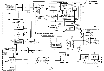
Figure l is a schematic diagram of the tester unit
according to a preferred embodiment of the present invention.
Figure 2 is a more detailed schematic diagram of the
feedback and status circuits as shown in Figure l.
Figure 3 is a more detailed schematic diagram of the
variable frequency generator and demodulator as shown in
Figure 1.
DETAILED DESCRIPTION OF THE PREFERRED EMBODIMENTS
Referring to Figure l, a modular test unit includes a
main frame unit ll, a source module 10 and detector module
12. An optical cable 15 is connected to source module 10 at
13 and to detector module 12 at 14. The main frame test unit
11 includes a microprocessor 18, a frequency generating
circuitry for providing a modulating frequency for the source
module 10, and an identifying and demodulating circuitry for
identifying the modulating frequency of the signal received
by the detector module 12, and demodulating the signal for
further processing for input into the microprocessor 18.
Each main frame unit 11 includes a microprocessor 18 for
controlling the various analog circuits, for storing
calibration parameters and for determining the power loss of
a transmitted light wavelength signal. The analog circuitry
of the main frame unit ll, the detector module 12, and source
module 10, are interfaced through an I/O board lll to the
microprocessor 18.
~3~1 1473
The source module 10 includes a light source 28 having a known
center wavelength of light output. The source module 10 receives
a specified modulation frequency from the mainframe unit for
providing signature modulation, e.g. modulating a known wavelength
of light by a known modulating frequency. Each source module is
assigned a different modurating frequency, depending upon its
wavelength, its type of source, e.g. laser or LED and the
calibrated output power. This modulating frequency assignment is
stored in each tester~s microprocessor~s memory 17. In order to
insure accuracy of testing by simulating normal operational
conditions for fibs-r optic cable systems which use either laser or
LED light sources for their data transmissions, source modules 10
are available which include LED light sources or laser light
sources.
The detector module 12 includes microprocessor controlled
circuitry for detecting the modulated light signal of a specific
wavelength and amplifying the sarne for receipt by the demodulator
circuitry 23 in the main frame unit 11. Because the detector
modules 12 each have their own varying responses to different
wavelengths of light received, each module 12 is calibrated at the
factory for determining this response, which response is stored in
the respective PROM's 75 located in the detector module 12. Upon
the demodulator 23 in the main frame unit 11 determining the
modulating frequency received by the detector module, the
microprocessor 18 will match the frequency with its assigned
13~ 73
wavelength of light. The microprocessor 18 will then retrieve
from the detector module PROM 75 the corresponding calibrated
parameters associated with the detector's responsiveness to the
light wave received, and will use these parameters in any
calculations the microprocessor will perform regarding the
received signal. ~
The tester unit is capable of measuring the optical power of
the transmitted light signal received at a second position, or it
can determine the power loss of a transmitted light wavelength
signal by comparing the power level of the received signal with
the power level of a reference signal. The comparison of signals
is performed by the microprocessor 18 with the reference signal
having been stored in the microprocessor's memory.
By flipping a switch (not shown) on the front panel of the
main frame unit 11, the operator may choose between a relative or
absolute mode for determining the power loss measurement. In the
relative mode, the tester is set up to make a power measurement of
any received signal and use this measurement as a relative value
for comparing with a second received signal. In an absolute mode,
the microprocessor uses as a reference signal, stored information
regarding the specific light wave which was transmitted. Each
tester main frame unit 11 has stored in its memory the power
intensities of all available light signal transmissions. Thus,
upon the demodulator circuitry 23 identifying the modulating
frequency, the microprocessor retrieves from its memory the
-- 10 --
~3~1~73
reference signal corresponding to the transmitted light wavelength
signal and uses the same for determining the received light
wavelength signal's power loss.
0~
In ~ preferred embodiment, the source module 10 transmits an
AC signal having a DC bias. The tester s~stem provides the
ability to measure the DC-optical power by filtering out the AC
components, or it can measure the peak AC power of the received
signal for determining the power loss associated with the same.
By attaching or removinq different source and detector
modules, the configuration of the test system can be changed. By
including both source 10-and detector 14 modules in a signal test
unit, the tester is set up in a local mode, whereby the tester
provides a test signal at the source module output 28 to a first
end 13 of a fiber optic cable 15 and detects the transmitted
signal at a second end 14 of the fiber optic cable 15 by an input
to the detector module 74.
If the fiber optic cable 15 under test is too long for local
or single tester applicability, a second main frame unit (not
shown) will be required at the second end of the fiber optic cable
15 under test. In this remote mode of testing, the first main
frame unit 11 with a source module 10 can be set up to transmit
the test signal to the first end 13 of the cable 15. The second
main frame unit tnot shown) is set up as the receiver requiring
only a receiver module 12 for detecting and measuring the power of
the received wavelength test signal. The second main frame uses
~3~1473
its microprocessor to identify the signature of the transmitted
signal and provides the appropriate controls and reference signal , ,_
for the detector module. If source 10 and detector 12 modules are
duplicated in both main frame units, the test signal may be sent
in either direction of the cable length, thereby providing a
testing system having bi-directional test capabilities.
The modularity of the testing system also allows for the
interchangability of different source modules 10, having different
wavelength test signals. This allows for a fle~ibility in testing
any number of available wavelengths by merely interchanying the
source module 10.~ Each dëtsctor module 12 is calibrated at the
factory for responding,to all available light sources. A
modulating AC signal is generated by a microprocessor controlled
frequency generator 16'located in the main frame 11 of the tester
unit. ,The frequency of the modulating AC signal is controlled by
data signals received from the microprocessor 18 through I/O ports
20a and 20~ of the microprocessor 18 and generator 16
respectively, In the preferred embodiment shown, the frequency
generator 16 provides a nominal output frequency of 10 KHz. The
output of the frequency generator 16 is provided to an input of a
phase lock loop (PLL) 22 having a voltage control oscillator
(VCO), as well as to an input to a demodulator and low pass filter
23. The output of the PLL 22 provides an AC signal of a known
frequency-to the input of a voltage control amplifier (VCA) 24
which serves as the input to the source module 10. The VCA in
- 12 -
13~ 73
turn provides an AC signal of a specified average voltage to a
driver circuit 26. The output of the PLL 22 is also provided at--a--
terminal 2~ on the rear panel of the main frame unit 11 for
referencing the AC signal, The driver circuit 26 then provides a
light source 28 with a nominal bias current having frequency
corresponding to the frequency of the AC signal provided by the
frequency generator 16, an average AC power determined by the VCA
24 and a DC bias level determined by the driver circuit 26. The
light source 28 comprising either a laser or light emitting diode
(LED), then provides a modulated light signal of a known
wavelength modulating fre'quency and power level to the fiber optic
cable 13.
The output of the light source 28 is provided as a feedback
circuit to control the light source. If a laser source is used, a
photodetector 30 senses the output of the laser and provides it on
line 33b to switch 33 which is connected during assembly of the
source module. If a LED is used as a source, a current measuring
circuit 31 is provided and connected to line 30a. The selected
feedback signal is provided to the AC level set circuit 32 which
should adjust the gain of the VCA 24 and to DC level set 34 to
adjust the driver circuit 26. A temperature compensation circuit
58 is also provided to control the temperature of either laser or
LED sources 28. Status circui,try 59 is connected to the
temperature compensation circuit 58, the DC level circuit 34 and
the AC level circuit 32 to provide a visual indication of the
-- 13 --
'~ .
,
., , ' .'
- i3~1473
proper operating status of this system as well as communicating
the status to the CPU via I/O port 20d. ----~ ~~~~~~~-~ ~~ ~~ ~
A source identification circuit 47 is included in every source
module 10 to identify to the main frame tester unit 11 the type of
light source the particular source module 10 represents via I/O
port 20e. The microproces~sor 18, can therefore, retrieve from its
memory, the necessary data for programming the respective
components of the source module 10 via I/O ports 20.
The details of the feedback and status circuitry are
illustrated specifically in Figure 2. The DC level set circuit 32
includes a low pass filter 35 and an integrator 36. Their output
is provided to a window detector 37 in the status circuitry 59.
If the signal is within the high and low value determined by the
window detector 37, a positive indication is given on terminal
20dl t.o the CPU. The AC level set circuit 34 includes a full wave
rectifier 38 and an integrator 39 providing a signal to window
detector 40 of the status control circuitry 59. If this value is
within the high and low limits set by the window detector, it will
provide a positive output on terminal 20d2 to the I/O port. The
visual indication in LED 64 is connected to the terminal 20d2 and
is lit if the DC level is within the acceptable limits.
The temperature compensation circuit 58 is included in the
source module 10 when a laser or LED source is used, for
maintaining a preselected temperature surrounding the laser or LED
source 28. In the preferred embodiment, a temperature of
- 14 -
~ 3U1~73
appro~imately 25C is maintained about the light source. The
compensation circuit 58 includes a resistive bridge 60 including-a - -
thermistor RT. An integrator 61 connected across the output of
resistor bridge 60 provides an input to the control circuit 62 for
peltier 45 for heating or cooling the light source and an input to
window comparator 63 of the status circuitry 59. The control
circuitry 62 for the peltier 45 is constructed as a current
switching bridge including serially connected P-channel transistor
41 and N-channel transistor 42 in parallel with series connected
P-channel transistor 47 and N-channel transistor 48 between a
current limiter and ground. The peltier device 45 is connected
between the two parallel iegs.- The output from the integrator 61
is provided as an input to the gates of the transistor pairs 41
and 42 via amplifier 43. The signals on the drain of the
transistor pairs are provided as a second input to the amplifier
43. A capacitor 46 is connected between the gates and sources of
the transistors 41 and 42 for providing stability. The output of
integrator 50 is connected as an input signal to amplifier 49, and
in turn, the output of amplifier 49 is connected to the gates of
transistor pair 47 and 48. The sources of the transistor pair 47
and 48 are also connected as a second input to the amplifier 49.
A capacitor 51 is connected between the common gates and sources
of the transistor pair 47 and 48 for providing stability.
Depending upon the high or low value of the output signal sensed
by the resistor bridge 60, diagonally opposing transistors of the
~3~ 73
control circuit will be activated to control the degree and
direction of current through the peltier device. For current in.. ...-..
one direction, the peltier device will heat up and for current in
the other direction, it will cool. By way of e2~ample, if a
positive signal is provided on amplifier 43, the N-channel device
42 will be on and the P-channel device 41 will be off. The
inverted signal on amplifier 49 will turn on P-channel device 47
and turn off N-channel device 48. Thus, the current path will be
from the voltage regulator 44 through P-channel device 47, laser
peltier 45, N-channel devlce 42 to ground. The low voltage signal
at the source of 42. is .fed back to amplifier 43 to further
increase its differential as will the current signal on the source
of transistor 53 be provlded to the amplifier 49.. For a low input
signal, the inverse occurs, namely P-channel 41 and N-channel 48
are on providing a current path through peltier 45 in the opposite
direction. The inverted and non-inverted input signals are
provided to the window detector 63 which provides an output signal
to I/O port 20d2 as well as to the LED 64.
The detector module 12 of the receiving part of the test
system includes a photodetector 74 arranged at a second end 14 of
the fiber optic cable 15. A detector prom module 7S is included
in each detector module 12 for storing information relating to the
responsivity of the specific photodetector 74 to different
wavelengths of light, also gain, absolute calibration factors,
type of detector, and parity checker bits. Because the
- 16 -
.
13~1473
photodetector 74 will respond differently to different wavelengths
of light, the detector 7~ is tested during the manufacturing-and~
assembly of the detector module i2 for determining this variance,
with the resulting information stored in the detector prom 75.
This information is retrieved by the microprocessor 18 via I/O
port 20f from the detector- prom 75 during the normal testing
operation as compensating factors in order to eliminate the
responsivity of the photodetector 74 to light wavelengths in
determining the power of attenuation of the test signals.
The photodetector 74 provides a current equivalent to the
power intensity of the det~ected transmitted si-gnal to a
microprocessor controlied variable gain current-to-voltage I/V
converter 76. The microprocessor 18 via D/A converter 79 and I/O
ports 20g controls the reference signal for I/V converter 76 and
via I/O 20h the gain of resistors 77 by switchinq different
resistors into the feedback of the I/V converter 76. The output
of the I/V converter 76 is then supplied either directly to
amplifier 80 whose gain is microprocessor controller via I/O 20i
or supplied indirectly to the same via amplifier 78, as determined
by switch 82 controlled by I/O 20j. The output of amplifier 80 in
turn provides the input to a demodulator 84 located in the main
frame test unit 11. Additionally, this output is provided to a
speaker 92 via serially connected voltage control oscillator 88
and buffers 89. An output of a demodulator 23 in the main frame
11 provides the input to a continuity indicator circuit 86 located
- 17 -
~3~473
in the detector module 12. The indicator 86 includes an LED for
indicating the presence of a detected signal by photodetector 74.
The demodulator 23 receives an AC reference signal from the
frequency generator 16. In local mode, the transmitter and
receiver components are in one unit and, thus, the demodulator 23
merely references the output of the frequency generator 16 to
determine the frequency of modulation. In remote mode, the main
frame unit which is at the receiving end of the cable, does not
have this initial information, and thus, must step the frequency
generator 16 through all the possible modulating frequencies of
the transmitter which a.re''~stored in the microprocessor~s memory in
the receiving unit,'and compare the same with the received signal
to determine the AC modulating frequency of the transmitter. The
demodulator 23 then receives the necessary frequency components.
The output of the demodulator 23 provides the input to a
sample and hold circuit 101 and A/D converter 102. The A/D
converter 102 in turn provides the input to a buffer and decoder
104 and to an alphanumeric display 106. The buffer and decoder
104 is further coupled to a data bus 108 which connects to the I/O
circui-t 111 and General Purpose Interface Bus (GPIB) 112. The I/O
circuit 111 is also coupled to the central processing unit (CPU)
18.
Figure 3 shows a more detailed schematic diagram of a
preferred embodiment of the frequency generator 16 and demodulator
23. The frequency generator 16 includes a temperature compensated
- 18 -
13~1473
crystal oscillator (TCXO) 16 which provides the input, e.g. 10 KHz
to a first microprocessor controlled multiple divider 118 having - --
I/O ports 20a connected to the microprocessor 18. In the
preferred embodiment, the multiple divider 118 provides assigned
frequencies in steps of 40 Hz from the nominal frequency of 10 KHz
for assigning a specific AC frequency of modulation to each
wavelength of light to identify the wavelength with a signature or
identifying AC frequency. The output of the multiple divider 118
is then provided to a divide-by-four divider 120 for providing an
output signal to the PLL circuit 22 and frequency components q, q,
i, i representing-the generated frequency to the demodulator 23.
The demodulator 23-includes an amplifier 122 whose output is
connected to ground via variable resistance 124 for providing DC
gain, and via capacitancë 126 and variable resistance 128 for
providing AC gain. A circuit for providing the equivalent peak
value of the received AC component is connected between the output
connections of amplifier 122 and the sample and hold circuits
101. This circuit comprises parallel mixers 130 and 132 having
inputs connected to the respective output signals of the
divide-by-four divider 120 or to the microprocessor, depending
upon the mode the system is operating under. The mixers 130, 132
have a common connection with variable resistance 128 for
receiving the received transmitted signal from amplifier 122. The
respective outputs of mixers 130, 132 are connected to respective
microprocessor controlled low pass filters 134, 136 and to
,
.
.
13~ 73
respective amplifiers 138, 140. The output of the amplifiers 138,
140 provide the Q and I components respectively, which are then~
provided to respective inputs to the sample and hold circuit lOl,
and A/D converter 102, respectively of Figure 1.
In the operation of the measuring system, the frequency
generator 16 is programme~ to produce a specific frequency
output. The frequency output of the generator 16 will then be
processed through the phase lock loop 22 and further processed by
a voltage control amplifier 24 and driver circuit 26. A bias
current provided by the driver circuit 26 will modulate the light
source 28 at the assigned frequency of the generator's output, and
at the power intensity provided by the VCA and driver circuits.The
light source 28 comprises either a laser or LED having a known
central wavelength associated with its light signal output. The
source module 10 includes at lèast one of these light sources 28
with each of the sources providing a light signal of a distinct
central wavelength. The microprocessor 18 programs the frequency
generating system 16 to generate a specific frequency to
corr~spond to each of the light sources 28, thereby providing an
identification or signature modulation for the particular light
wavelength of each source. Because the modules and main frame
units are calibrated to a common standard in the loss absolute
mode of measurement, further calibration is no longer required of
the tester system in the field or in the lab.
- 20 _
~.3~1473
A photodetector 30 is arranged near the light source 28 or a
current senser 31 for providing a feedback signal to the~
respective AC and DC level controls, 32, 34. The respective
circuits provide for stabilizing the amplitude and frequency of
the AC signal by controlling the AC level of the VCA 24 ~nd the DC
level of the driver circuit 26. The status circuit 59 receives
output signals from the feedback circuits 32, 34, 58 and compares
the sum of the output signals for comparing with maximum and
minimum parameters provided in each feedback circuit. If the
status signal falls outside the limit of the parameters of the
comparator circuits, an LED 63 will light up and the
microprocessor will provide a message on the display means 106
indicating that the status of the transmitter is out of
specification.
Once the modulated light signal is transmitted through the
fi~er cable 15, the photodetector 74 of the detector module 12
detects the signal at a second end 14 of the fiber cable 15 and
converts the light signal into an equivalent current signal. This
current signal is then supplied to a microprocessor control
current-to-voltage converter 76. The output voltage of the
amplifier 76 is directed to microprocessor controlled-amplifiers
78 and 80 which serve as an auto-ranging circuit.
The output of amplifier 80 provides the input to a demodulator
23, and the voltage control oscillator (VCO) 88. The VCO drives a
speaker 92 via buffer 89 for aurally indicating the signal
strength received at the photodetector 74.
- 21 -
.
~ ,
:
-
- 13V14~3
If the apparatus is set up in a local or internal mode e.g.
having only a single unit, then the necessary information for~
determining a frequency of modul~ation or demodulating the received
signal in the modulator 23 is provided directly from the frequency
generator 16. If the apparatus is operated in a remote or
e~ternal mode e.g. having two separate units for the transmitter
and receiver, then the receiving unit's microprocessor 18 will
step its frequency generator 16 through the various frequency to
determine a match and lock it in to provide the necessary signals
to the receiving unit demodulator 23.
Upon identifying the-modulating frequency, the microprocessor
in the receiver.main frame unit 11 will provide through respective
I/O ports 20a the necessary signals for adjusting.the gain of
respective current-to-voltage amplifier 76 in the detector module .
12. Additionally, the microprocessor 18 will identify from its
memory the particular light wavelength assigned to the detected
modulating freguency, and thereby incorporate compensating
parameters from the detector PROM 75 of the detector module 12
which correspond to the specific photodetector's 74 responsivity
to that particular light wavelength.
The demodulation and low pass filter 23 will provide the
equivalent peak value of the received modulating signal in the
external mode. These values are determined originally during the
manufacturing and calibration process of the apparatus system, and
stored within the microprocessor's memory for each assigned
'
. ~ - 22 -
~ ' .
~3~ 73
frequency. The output of the demodulator and low pass filter 23
will then be supplied to a sample and hold 101 and an~
analog-to-digital converter 102. This information is further
processed by the microprocessor 18 by comparing the received
values corresponding to the power intensity of the received signal
to that of a reference signal stored in the microprocessor 18.
This reference signal may be an absolute value determined during
the calibration of the system at the assembly plant, or may be a
relative value determined by testing a reference cable immediately
before the present test for using the result of the reference
cable as a relative value. The microprocessor 18 will calculate
the difference between thë received transmitted signal of known
wavelength of light and the reference value for determ1ning the
attenuation associated with the transmission of the particular
light wavelength. This attenuation will then be displayed on the
display means 106 and may be stored within the microprocessor's
memory for further analysis. The microprocessor will then start
the above procedure over for new wavelengths of light transmitted
by a new laser or LED source. Also, through the use of the
General Purpose Interface Bus (GPIB), the resulting information
may be outputted to a printer or other digital contrclled
mechanism.
Although certain preferred embodiments provide for modulated
light signals having the same power levels prior to transmission,
the tester is capablé of having varying power levels assigned to
the specific modulated light signals.
- 23 -
~.3~ 73
From the preceding description of the preferred embodiments,
it is evident that the objects o the invention are attained,--and
although the invention has been described and illustrated in
detail, it is to be clearly understood that the same is by way of
illustration and example only and is not to be taken by way of
limitation. The spirit a~d scope of the invention are to be
limited only by the terms of the appended claims.
- 24 _