Note: Descriptions are shown in the official language in which they were submitted.
~3~330
OPEN LOOP MOTOR CONTROL WITH
BOTH VOLTAGE AND CURRENT REGULATION
1. Field of the Invention
The field of the invention is AC motor drives for
variable speed control of AC induction motors, and more
particularly, AC motor drivea using pulse width modulation
(PWM) techniques.
2. Description of the Background Art
A PWM motor drive for an AC induction motor includes a
power section and a logic and control section. The power
section includes the high voltage and current devices to
convert AC inpu~ power to DC power and then, to convert the
DC power to a variable frequency, PWM voltage for input to an
AC motor. The logic and control section includes the low
power signal processing circuits and logic circuits which
control the performance characteristics of the drive. The
user of the drive sets certain operating parameters through
input devices interfaced to the logic and control section.
In the power section a PWM voltage inverter receives
power from a 3-phase AC source operating at 60 Hz frequency.
TAe AC power is converted to DC power to provide a source for
synthesizing voltages of different frequencies which are
necessary to control speed in an AC motor.
The pulse train pattern from a PWM inverter is
characterized by a first set of positive pulses of equal
magnitude but of varying pulse width and by a second set of
13~1~3(~
negative-going pulses of equal magnitude but of varying pulse
width. The RMS value of this pulse train pattern
approximates one cycle of a sinusoidal signal which is
characteristic of an AC waveform. The pattern is repeated to
generate additional cycles of the AC waveform.
To control the frequency and magnitude of the resultant
AC power signals to the motor, control signals from the logic
and control section are applied to the PWM inverter.
AC motor control systems that incorporate PWM drives,
can be categorized as follows: 1) a closed-loop type in which
the speed of the motor is sensed with a tachometer and fed
back to determine an error signal which is applied to reduce
the difference between a commanded speed and the actual
speed, and 2) an open-loop type which does not include a
tachometer for sensing the actual speed of the motor.
The advantage of the open-loop type is lower cost, in
that the tachometer is a relatively sophisticated and
expensive accessory to the basic motor control. The
tachometer is also sometimes difficult to connect and may
cause a decrease in overall system reliability. Controls
without speed sensing are considered to be "open-loop", even
though other parameters such as voltage or current may be
sensed.
To drive a PWM voltage inverter the motor control
provides an AC command signal of a certain magnitude and
frequency. In one type of open-loop control, slip is roughly
determined and frequency is more closely determined by
predefined speed profiles, referred to as "accel/decel" rates
which are selected and adjusted through switches interfaced
to the logic and control section of the motor control. The
--2--
~3~
speed commands are translated into torque commands by
applying a specified volts/hertz ratio, which can be selected
through a user-selectable switch or a jumper wire interfaced
to the logic and control section of the motor control.
A PWM voltage inverter provides fast transient response
to load disturbances which is a significant advantage. A
second advantage is that velocity feedback is not necessary
to reach a stable steady-state operating condition. However,
there are times, when starting the motor or when strong load
disturbances occur, when current to the motor may become
excessive.
One way of controlling current at startup is to provide
a current regulator which compares a commanded current to the
actual current and generates an error signal to the PWM
inverter to reduce the error. A current-regulated PWM
(CRPWM) drive, however, does not respond as quickly as a
voltage inverter to sudden and substantial load disturbances.
For overcurrent protection in a voltage inverter drive,
a circuit is available for monitoring current to the motor
and according to the specific condition either shutting down
the motor or pr.oviding a controlled slow-down and
re-acceleration to operating speed. This solution has not
entirely eliminated undesirable torque oscillations during
certain extreme loading conditions. Also, during light
loading, it has been found that the motor may be overexcited
resulting in inefficient performance. Still further, the
shutting down of the motor in response to load disturbances
is in some instances an unnecessary inconvenience to the
motor user.
Thus, it is an object of the present invention to
~3~E33~3
improve the response and control capabilities of an open-loop
PWM motor control without increasing its production cost by
an amount comparable to the cost of adding speed sensing
equipment.
Sum~u~of the I~venti2n
The invention relates to a motor control in which a
voltage control loop is closed around a current regulator
portion of a current-regulated pulse width modulation (CRPWM)
drive. This provides a hybrid control, which in comparison
with the unmodified CRPWM drive, provides improved startup,
improved response to light load conditions and improved
response to sudden load disturbances.
The control includes a PWM voltage inverter for
generating a pulse width modulated voltage signal to be
applied to an induction motor in response to a DC voltage
signal from a DC power source and in response to an AC
voltage command signal.
The control also includes a current regulator for
generating the AC voltage command signal to control the PWM
voltage inverter. The current regulator generates the AC
voltage command signal to the PWM inverter in response to an
AC current command signal and in response to a feedback
signal representative of actual current being supplied to the
motor.
The control also includes a voltage regulator which
controls the command to the current regulator in response to
the output voltage of the current regulator. That output
voltage is representative of motor terminal voltage, so that
both voltage and current at the motor terminals are sensed.
13~ 330
In accordance with an embodiment of the
invention, a pulse width modulation (PWM~ motor control
for sensing the rotational speed of the motor, the
control is comprised of current regulation apparatus
S for generating AC inverter voltage control signals; a
PWM voltage inverter with outputs for electrical
connection to the induction motor, the PWM inverter
being responsive to a DC voltage signal from a DC power
source and responsive to AC inverter voltage control
signals from the current regulation apparatus to
generate a voltage that is applied to the induction
motor during operation of the induction motor; voltage
feedback apparatus for sensing changes in the voltage
applied to the induction motor during operation of the
induction motor; conversion apparatus coupled to the
voltage feedback apparatus for converting the changes
in the voltage sensed through the voltage feedback
apparatus to a corresponding plurality of digital
voltage feedback values; microelectronic processing
apparatus coupled to the conversion apparatus for
calculating a single DC value for voltage feedback in
response to the plurality of digital voltage feedback
values; voltage regulation apparatus for controlling AC
current command signals to the current regulation
apparatus in response to the DC value for voltage
feedback; and wherein the current regulation apparatus
generates the AC inverter voltage control signals in
~L3~ 33(~
response to t.he AC current command signals and in
response to current feedback signals that are in turn
responsive to actual current being supplied from the
outputs of the PWM voltage inverter.
In accordance with another embodiment, a
pulse width modulation tPWM) motor control for improved
control of current to an induction motor without
sensing the rotational speed of the motor, the control
is comprised of current regulation apparatus for
0 generating AC inverter voltage control signals in q-
axis and d-axis components; a PWM voltage inverter with
outputs for electrical connection to the induction
motor, the PWM inverter being responsive to a DC
voltage signal from a DC power source and responsive to
the AC inverter voltage control signals in q-axis and
d-axis components to produce a voltage that is to be
applied to the induction motor during operation of the
induction motor; voltage feedback apparatus for sensing
a change in the voltage applied to the induction motor
~0 during operation of the induction motor; conversion
apparatus coupled to the voltage feedback apparatus for
converting the change in the voltage sensed through the
voltage feedback apparatus to digital voltage feedback
values; microelectronic processing apparatus for
generating AC values for motor voltage in response to a
predetermined acceleration/deceleration rate and in
response to a predetermined volts/hertz ratio; AC
- 5b -
~3~1830
voltage regulation apparatus for controlling AC current
command signals in q-axis and d-axis components to the
current regulation apparatus in response to the AC
values generated by the microelectronic processing
apparatus and in response to the digital voltage
feedback values received from the conversion apparatus;
and wherein the current regulation apparatus generates
the AC inverter voltage control signals in q-axis and
d axis components in response to the AC current command
signals in q-axis and d-axis components and in response
to current feedback signals that are in turn responsive
to actual current being supplied from the outputs of
the PWM voltage inverter.
In accordance with another embodiment, a
pulse width modulation (PWM) motor control for improved
control of current to an induction motor without
sensing the rotational speed of the motor, the control
is comprised of current regulation apparatus for
generating AC inverter voltage control signals, the
current regulation apparatus having outputs at which
the AC inverter voltage control signals are generated,
and wherein the AC inverter voltage control signals
vary 90 in phase; a PWM voltage inverter with outputs
for electrical connection to the induction motor, the
PWM inverter being responsive to a DC voltage signal
from a DC power source and responsive to the AC
inverter voltage control signals to produce a voltage
- 5c -
131}~330
that is applied to the induction motor during operation
of the induction motor; voltage feedback apparatus for
sensing changes in the AC voltage applied to the
induction motor during operation of the induction
S motor; conversion apparatus coupled to the voltage
feedback apparatus for converting the changes in the AC
voltage to a plurality of digital voltage feedback
values; microelectronic processing apparatus coupled to
the conversion apparatus, wherein the microelectronic
processing apparatus includes apparatus for calculating
DC feedback values from the digital voltage feedback
values, and wherein the microelectronic processing
apparatus includes apparatus for generating two DC
command signals corresponding to the AC inverter
control signals which vary 90 in phase; voltage
regulation apparatus for controlling AC current command
signals to the current regulation apparatus, wherein
the DC feedback values are compared with the two
respective DC command signals generated by the
microelectronic processing apparatus; and wherein the
current regulation apparatus generates the AC inverter
voltage control signals in response to the AC current
command signals and in response to feedback signals
that are in turn responsive to actual current being
supplied from the outputs of the PWM voltage inverter.
- 5d -
~3~J~1~30
rief Descri~tion of the,,,~rawing~
Fig. 1 is a circuit diagram of a first embodiment of the
invention in which a voltage regulator is an analog circuit;
Fig. 2 is a circuit diagram of a second embodiment of
the invention in which a DC voltage regulator is carried out
within a microelectronic processing circuit;
Fig. 3 is a circuit diagram of a third embodiment of the
invention in which an AC voltage regulator is carried out
within a microelectronic processing circuit;
Fig. 3a is a circuit diagram of a fourth embodiment of
the invention in which a second type of DC voltage regulator
is carried out within a microelectronic processing circuit;
Fig. 4 is a flow chart showing a program for carrying
out the embodiment of Fig. 2; and
Fig. 5 is a flow chart showing a program for carrying
out the embodiment of Fig. 3.
~3~1~3~;)
Detailed Descrip~iQ~ Qf the Preferred Emhn~ime~
Figs. 1-3 illustrate three embodiments of the invention.
All three relate to a current-regulated pulse width
modulation (CRPWM) motor control for an AC induction motor
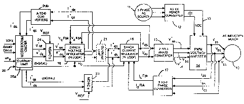
10. The motor control (also called a "drive"~ includes a
power section that receives power at a line frequency of 60
Hz from a 3-phase AC power source 11. The three phases of
the power source are connected to an AC DC power converter 12
in the power section of the drive. The AC-DC power converter
12 rectifies the alternating current signals from the AC
source 11 to produce a DC voltage (VDC) on a DC bus 13 that
connects to power inputs on the pulse width modulation (PWM)
voltage inverter 19, which completes the power section of the
drive. The AC source 11, the AC-DC power converter 12, and
DC bus 13 provide a DC source for generating a DC voltage of
constant magnitude. The PWM inverter 14 includes a group of
switching elements which are turned on and off to convert
this DC vol.tage to pulses of constant magnitude.
The pulse train pattern from a PWM inverter is
characterized by a first set of positive-going pulses of
constant magnitude but of varying pulse width and by a second
set of negative-going pulses of constant magnitude but of
varying pulse width. The RMS value of this pulse train
pattern approximates one cycle of a sinusoidal signal which
is characteristic of an AC waveform. The pattern is repeated
to generate additional cycles of the AC waveform.
To control the frequency and magnitude of the resultant
AC power signals to the motor, AC voltage command signals are
applied to the PWM inverter. The PWM voltage inverter 19
receives three balanced AC voltage command signals, V*aS~
V*bs and V*cs which vary in phase by 120~, and the magnitude
~3~183(~
and the frequency of these signals determines the pulse
widths and the number of the pulses in pulse trains VaSr VbS
and Vcs which are applied to the terminals of the motor. The
asterisk in the first set of signals denotes a "command"
signal. The "s" subscript in both sets of signals denotes
that these signals are referred to the stationary reference
frame, where the voltages would be the phase voltage signals
incorporated in the line-to-line voltages observed across the
motor terminals.
These AC voltage command signals, V*as/ V*bs and V*cs
are produced as a result of a 2-phase to 3-phase conversion
which is accomplished with a 2-to-3 phase converter 15. This
circuit is known in the art, and for the purpose of this
description it is sufficient to know that signals Vqs and VdS
are sinusoidal AC voltage command signals having a magnitude
and a frequency. These signals are related to a d-q
reference frame in which the phase angle of the q-axis
component and ~he phase angle of the d-axis component are 90
apart.
The AC voltage control signals Vqs and VdS are output
signals from a synchronous current regulator 16. The details
of this circuit 16 have been previously shown and described
in Kerkman et al., U.S. Pat. No. 4,680,695 issued July 14,
1987 The synchronous current regulator 16 includes a
proportional-integral loop with summing inputs. At one
summing input, an AC current command signal related to the
q-axis, I*qsr is algebraically summed with an Iq Fbk signal
related to the q-axis. At a second summing input, an AC
current command signal related to the d-axis, I*dS~ is
algebraically summed with an Id Fbk signal related to the
13~ 330
d-axis. The electrical operating frequency in radians (~e)
is also an input signal to both the q-axis and d-axis
branches of the circuit. With these input signals, the
synchronous current regulator 16 controls the AC voltage
command signals Vqs and VdS at its outputs in response to
current error, and further, it maintains the relationship of
the output signals to the d-axis and the q-axis.
To obtain the Iq Fbk and Id Fbk signals, current sensing
devices (not shown) are used to sense the phase currents Ia
IbS and Ics flowing to the motor terminals. These signals
are fed back to a 3-to-2 phase converter 17 for converting
these signals to feedback signals Iq Fbk and Id Fbk that are
related to the d-q frame of reference. Such circuits are
known in the art and the details are not essential to this
description.
Thus far, the description has related to elements which
are known in the art and which are shown in each of the three
examples in Figs. 1-3. The invention involves the addition
to the synchronous current regulator 16 of a voltage
regulator 18 and voltage control loop.
Referring to the first embodiment in Fig, 1, a
synchronous voltage regulator 18 is added to drive the
synchronous current regulator 16 and to produce AC current
command signals, I*qs and I*dS. The synchronous voltage
regulator 18 is connected to the synchronous current
regulator 16 through a current limit circuit21 which may be
a hardware circuit or which may be implemented by
executing a program 20a in a microprocessor 20. This first
preferred embodiment is based on the execution of the current
limit 20a in the microprocessor 20.
_9_
13~i~1330
The voltage regulator 18 contains the same circuitry as
the synchronous current regulator 16, and thus the circuit
disclosed in Kerkman et al., U.S. Pat. No. 4,680,695, cited
above, is used for this analog version of the voltage
regulator 18. The voltage regulator 18 receives AC voltage
command signals V*qs and V*dS and algebraically sums these
signals with feedback signals Vq Fbk and Vd Fbk for the
q-axis and d-axis, respectively. The feedback signals Vq Fbk
and Vd Fbk are the AC voltage command signals V*qs and V*dS
which are sensed at the outputs of the synchronous current
regulator 16 and returned through two circuit paths to
summing inputs within the voltage regulator 18. The
synchronous voltage regulator 18 also receives the electrical
operating frequency in radians (~e) in the form of digital
data from the microprocessor 20. This data is applied
through multiplier circuits within the regulator 18 as
described for the current regulator disclosed in Kerkman et
al., U.S. Pat. No. 4,680,695, cited above. With these
inputs, the voltage regulator 18 controls the AC current
command signals I*qs and I*dS at its outputs in response to
voltage error, and further, these output signals are referred
to the d-q axes.
Although this embodiment includes a synchronous voltage
regulator 18, a stationary voltage regulator can also be
used. With a stationary voltage regulator, the inputs are
the same as shown in Fig. 1, except that the input for ~e
would be dropped. This can be implemented in the circuit in
Fig. l by setting ~e = 0 at the output of the microprocessor
20. This eliminates a cross-coupled component from the
outputs from the voltage regulator 18, but the resulting
--10--
13~ l33(;)
stationary voltage regulator 18 is suitable for providing the
necessary current commands to the current regulator 16.
Before the signals from the voltage regulator 18 are
applied to the inputs of the current regulator 16, they are
subject to current limiting operations. To carry out this
operation in the microprocessor 20, the analog signals I*qs
and I*dS at the outputs of the voltage regulator 18 are fed
back to analog-to-digital converters 20b, where the signals
are converted to digital values for I*qs and I*dS for input
to the microprocessor 20. Many suitable analog-to-digital
converters 20b are known in the art. In this embodiment, the
analog-to-digital converters 20b may be integrated in a
single circuit with the microprocessor 20 where the
microelectronic circuit is the Model 8096 offered by Intel
Corporation of Santa Clara, California. The microprocessor
20 compares the commanded values for I*q, I*d with certain
maximum values, and if these maximum values are exceeded, the
values for I*q and I*d are reduced to the maximum current
limits. The microprocessor 20 then outputs the current-
limited values of I*q and I*d to a pair of multiplying
digital-to-analog converter (MDAC) circuits 23. A commercial
version of such a circuit is the AD 7529 multiplying
digital-to-analog converter offered by Analog Devices,
Norwood, Massachusets.
The microprocessor 20 generates digital values for I*q
or I*d which are instantaneous values of AC signals in the
form of I* cos ~e and -I* sin ~e, respectively. The series
of digital values follows the functions I* cos ~et and -I*
sin ~et. These values are multiplied by V RFF to arrive at
the proper signal level for input to the synchronous current
~3~L1330
regulator 16. Each MDAC circuit 23 multiplies a voltage
reference signal, v REF by a series of digital values for
I*qs or I*dS. The signals resulting from the conversion
through MDAC circuits 23 are designated I*qs and I*dS and are
S AC input signals to the synchronous current regulator 16.
The microprocessor 20 also generates digital values for
V*qs or V*dS which are instantaneous values of AC signals in
the form of V* cos ~e and -V* sin ~e, respectively. The
series of digital values follows the functions V* cos ~et and
-V* sin ~et. These values are transmitted via a digital data
bus to a second pair of MDAC circuits 24, where they are
multiplied by V REF to arrive at AC signals V*qs and V*ds of
the proper signal level for input to the synchronous voltage
regulator 18. The Model AD 7524 circuits mentioned above are
also suitable for use as the MDAC circuits 24.
The microprocessor 20 calculates the motor voltage
command values V*q and V*d in response to one of several
switch-selectable rates of acceleration and deceleration
(accel/decel rates). The switches are interfaced to the
microprocessor 20. The magnitude of the motor voltage
command is also determined by a voltage/hertz ratio, which is
a multiplier applied to the frequency determined by the
accel/decel rates. The voltage/hertz ratio is set to a
predetermined ratio by connecting a jumper wire on an input
interface so that an input signal is read by the
microprocessor 20. Another input to the microprocessor 20 in
Figs. 1-3 represents inputs from two potentiometers which
determine a range for the operating frequency ~*e , such as
0-90 Hz, for example, but expressed in radians (2~ x
frequency in Hz). Within this range the microprocessor 20
~3U1~330
generates various values of ~e as the motor is brought up to
a rated frequency such as 60 Hz for example.
The motor control system described in Fig. 1 exhibits
improved response to load disturbances because the voltage
regulator 18 senses a voltage drop at the motor terminals by
sensing a drop in voltages Vqs and VdS at the outputs of the
synchronous current regulator 16. A voltage drop at the
motor terminals is reflected back to the outputs of the
current regulator 16. A voltage feedback loop is closed
around the synchronous current regulator 16 with the input to
the regulator 16 being controlled by the voltage regulator
18. If a load disturbance calls for greater than maximum
current at a reduced voltage, thi.s is sensed at the outputs
of the current regulator 16 through the voltage regulator 18.
The current limiting circuit 20a, 21 limits current to the
maximum allowable current for the voltage at the motor
terminals. This limit is selected as something less than the
overcurrent which would cause the operation of an overload
protection circuit. Such an overload protection circuit
causes the shut down or other substantial interruption of
steady-state motor operation and it is an ob~ect of the
invention to provide a more refined response to transient
conditions than is presently available with the overload
protection circuit.
Referring next to Figs. 2 and 4, an alternative
embodiment of the same control arrangement provides fuller
utilization of a microelectronic processing circuit 20 to
reduce the analog circuitry in the system. In this
embodiment, the microelectronic processing circuit 30
includes a CPU (central processing unit) 30a and A-to-D
13~83~
converters 30b. The CPU 30a executes a program stored in
nonvolatile memory to emulate a DC voltage regulator 30c and
a current limit circuit 30d. In executing this program the
CPU 30a utilizes a random access memory (RAM) (not shown) to
store data and temporary results. The inputs to the
microprocessor for the volts/hertz ratio, accel/decel rates
and operating frequency ~e are the same as for the example
in Fig. 1. Also like the example in Fig. 1, the
microelectronic processing unit includes the CPU 30a and the
A-to-D converters 30b, and further is programmable to provide
a DC voltage regulator 30c and a current limit function 30d
to be described.
Referring next to Fig. 4, the CPU 30a executes a program
having a main program loop 40 for handling background
functions. Also during the main loop, the CPU 30a reads the
digital values for Vqs and VdS from the A-to-D converters
30b. As seen in Fig. 2, the A-to-D converters 30b receive
the analog feedback signals Vqs and VdS from the outputs of
the synchronous current regulator 16, as described for the
first example, and convert these to the digital values Vq Fbk
and Vd Fbk. These are read by the CPU 30a and saved in RAM
memory (not shown). Returning to Fig. 4, the reading of the
digital voltage feedback signals is represented by process
block 41 in the main loop 40 of the program executed by the
CPU 30a. As represented by decision block 41, when a timer,
which may be a programmable hardware timer or a si~ply a
timing routine in the program, times out and generates an
interrupt signal, the CPU 30a branches to an interrupt
portion of the microprocessor program. The beginning of this
interrupt portion is represented by process block 43, which
13~ 330
further represents the execution of instructions in the
program to update the operating frequency ~e, and the phase
angle of excitation, ~e, according to the following
equations:
~e(t) = ~e(t-1~ + ~e (1)
~e(t) = ~e(t-l) + ~e(t) ~T (2)
In equations (1) and (2), (t) is a present time and (t-
1) is a previous time. The accel/decel rate determines ~e
as a function of time, ~e is the phase angle or instantaneous
value for a function of the form sin ~e(t)~ and aT is the
elapsed time since the last update.
Next, as represented by process block 44, the CPU 30a
executes instructions to determine a DC value for a motor
voltage command V* according to the following equation:
V* = ~e(t)/2n x (V/ Hz) (3)
where (V/ ~z) is the volts/hertz ratio.
This value is compared against a voltage limit VmaX as
represented by decision block 45. If V* is greater than
VmaX~ as represented by the "YES" result, then V* is reduced
to VmaX as represented by process block 46. If V* is not
greater than VmaX~ as represented by the "NO" result, the
program proceeds directly to process block 47. As represented
by process block 47, the CPU 30a executes a subroutine which
retrieves the digital values for Vqs and VdS from memory,
squares each value, sums the two squared values and then
takes the square root of the sum to determine a single DC
magnitude for a feedback voltage, which shall be referred to
13~ 330
as VMAG.
Referring back to Fig. 2, it will be seen that the
voltage-limited value of V* and the value for VMAG are inputs
to the portion of the program that is executed to emulate a
DC voltage regulator 30c. The output of this regulator 30c
is a DC signal I*qe~ for commanding current from the
synchronous current regulator 16.
The I*qe signal is current-limited by executing the
current limit portion 30d of the program, and is then applied
to a DC-to-AC portion 30e of the program which converts the
I*qe signal to a pair of AC command signals I*q and I*d
having a phase difference of 90. The CPU 30a generates
digital values for ~e which are applied as a second input to
the DC-to-AC portion 30e of the program. The resulting
command signals I*qs and I*dS are then applied to a pair of
MDAC circuits 25 and multiplied by V REF to convert the
digital outputs of the microelectronic processing circuit 30
to analog signals for input to the synchronous current
regulator 16.
This is also represented in Fig. 4, where process block
48 represents the execution of program instructions to
perform the voltage regulation loop according to the
following equations:
I integ (t) = I integ (t-1) + KI (V* - V MAG) (4)
I*qe = I integ (t) + KP (V* - V MAG) (5)
where I integ (t) is the value of an integral at
some time "t" and I integ (t-1) is the value of the
integral at some earlier time "t-1",
where KI is a gain factor applied to the voltage
-16-
130~1~30
error, (V* - V MAG)~ and
where Kp is a proportional gain factor applied to
the voltage error.
Next in Fig. 4, as represented by decision block 49, the
DC value of the current command I*qe is tested to determine
if it is greater than a DC current limit I*q max- If I*qe is
greater than I*q max, as represented by the "YES" result,
then I*qe is reduced to I*q max as represented by process
block 50, and the program proceeds to process block 51. If
i*qe is not greater than I*q max, as represented by the "NO"
result, the program proceeds directly to process block 51.
As represented by process block 51, the AC output
ccmmands are formed according to the following equations:
I*q~ = I*qe x Cos (t~e) t6)
I*dS = ~I*qe x Sin (~e) t7)
The AC commands I*q and I*d are outputs from the
microelectronic processing circuit 30 to the MDAC circuits 25
in Fig. 2. As represented in Fig. 4 after the AC current
cornmands have been formed and transmitted, as represented by
I/O block 52, the CPU 30a returns from the lnterrupt portion
of the program to the main loop 40.
The motor control system described in Fig. 2 responds to
a voltage drop at the motor terminals by sensing a drop in
voltages Vqs and VdS at the outputs of the synchronous
current regulator 16. A voltage feedback loop is closed
around the synchronous current regulator 16 with the input to
the regulator 16 being controlled by a microelectronic
processing circuit that emulates the voltage regulator 30c.
-17-
13(~ 3(~
If a load disturbance ealls for greater than maximum current
at a reduced voltage, this is sensed at the outputs of the
current regulator 16 through the voltage regulator 30e. The
current limiting portion 30d of the processor operation
limits current to the maximum allowable current for the
voltage at the motor terminals. This limit is selected at
something less than the overcurrent which would cause the
operation of an overload protection circuit.
Fig. 3 shows a third embodiment of the invention in
which a microelectronie processing unit 35 executes
instructions to provide voltage regulation of AC quantities.
In this embodiment, the mieroelectronie processing eircuit 35
lncludes a CPU (central proeessing unit) 35a and A-to-D
converters 35b. The CPU 35a exeeutes a program stored in
nonvolatile memory (not shown) to emulate an AC voltage
regulator 35c and a current limit eireuit 35d. In executing
this program the CPU utilizes a random access memory (RAM)
(not shown) to store data and temporary results. The inputs
to the CPU 35a for the volts/hertz ratio, accel/decel rates
and operating frequency ~*e are the same as for the example
in Figs. 1 and 2. Also like the example in Fig. 2, the
microelectronic processing unit includes the CPU 35a and the
A-to-D converters 35b, and further is programmable to provide
an AC voltage regulator 35c and a current limit circuit 35d
to be described.
Referring also to Fig. 5, the CPU 35a also executes a
program having the main program loop 90 for handling
background functions. Also during the main loop, the CPU 35a
reads the digital values for VqS and VdS from the A-to-D
converters 30b, which are designated Vq Fbk and Vd Fbk in
-18-
:~3~83V
Fig. 3. As seen in Fig. 3, the A-to-D converters 30b receive
the analog feedback signals Vqs and VdS from the outputs of
the synchronous current regulator 16, as described for the
previous example, and convert these to the digital values Vq
Fbk and Vd Fbk. These are saved in RAM memory (not shown)
for later use in executing the AC voltage regulator function.
Returning to Fig. 5, the reading of the voltage feedback
signals is represented by process block 91 in the main loop
40 of the program executed by the CPU 35a. As represented by
a decision block 42, when a timer, which may be a
programmable hardware timer or a simply a timing routine in
the program times out and generates an interrupt signal, the
CPU 35a branches to an interrupt portion of the
microprocessor program. The beginning of this interrupt
portion is represented by process block 53, which further
represents the execution of instructions in the program to
update the operating frequency ~e, and the phase angle of
excitation, ~e, according to equations (1) and (2) set forth
earlier in this description.
Next, as represented by process block 54, the CPU 35a
executes instructions to determine a DC value for a motor
voltage command V* according to equation (3) set forth
earlier in this description, by multiplying the frequency
determined from the accel/decel rate by the volts/hertz
ratio.
This value is compared against a voltage limit VmaX as
represented by decision block 55. If V* is greater than
Vmax, as represented by the "YES" result, then V* is reduced
to VmaX as represented by process block 56. If V* is not
greater than VmaX~ as represented by the "NO" result, the
--19--
83~
program proceeds directly to process block 57. As
represented by process block 57, the CPU 35a executès
instructions to form AC motor voltage commands related to the
q-axis and to the d-axis according to the following
equations:
V*qs = V* Cos (ae) (8)
V*dS = -V* Sin (ee) (9)
As seen in Fig. 3, V*qs and V*dS become the inputs to
the voltage regulator portion 35c of microprocessor
operation. The outputs of this regulator 35c are AC signals
I*qs and I*dS for commanding current from the synchronous
current regulator 16. The I*qs and I*dS signals are
current-limited by executing the current limit portion 35d of
the microprocessor program, and are then output to the MDAC's
25 which convert the digital output commands to analog
command signals I*qs and I*dS which are applied to the
synchronous current regulator 16.
The execution of an AC voltage regulator 35c is also
represented in Fig. 5, where process block 5~ represents the
execution of program instructions to perform the voltage
regulation loop. For a synchronous AC voltage regulator, the
voltage regulation loop is executed according to the
following state equations:
(d/dt)XqdS = KI (V*qds - V qds) + [~eX] Xqds (10)
I*qds = Xqds + Kp (V*qds - V qds) (11)
where I*qds represents the two commands I*qs and
I*dS~ V*qds represents the two commands V*qs and V*ds,
and V qds represents the two feedback signals for Vqs
-20-
~C~:1830
and VdS,
where KI is a gain factor applied to integration of
voltage error, (v*qds - V qds)r
where Kp is a proportional gain factor applied to
the voltage error,
where Xqds represents an auxiliary system state (a
mathematical expression) for the motor control system,
and
where [~ex] represents a frequency-dependent
multiplier which may be represented as a 2 x 2 matrix
with terms ,~e,~~e and 0,respectively.
For a further explanation of the formulas and theory for
the synchronous current regulator which is applied here to
the regulation of voltage, reference is made to Rowan and
Kerkman, "A New Synchronous Current Regulator and an Analysis
of Current Regulated PW~ Inverters" IEEE Tra~ ~n Industry
Appl-ca~iQ~ IAS Vol. lA-22, No. 4, July-August 1986 pp. 678- -
690.
A stationary regulator could also be used for the AC
voltage regulator 35c of Fig. 3. In such a case, equations
10) and 11) above would also apply for execution of the
voltage loop, except that the term [~ex] Xqds in equation 10)
would be zero. In Fig. 3, the dashed arrow input to the
voltage regulator 35c for ~e represents the optional nature
of this input according to whether the synchronous or
stationary (~e = 0) regulator is selected.
Next in Fig. 5, as represented by decision block 59, the
magnitude of the current command I*qs is tested to determine
if it is greater than a current limit I* max- If I*qs is
greater than I* max, as represented by the "YES" result, then
-21-
~3~ 30
I*qs is reduced to I* max as represented by process block 60,
and the program proceeds to process block 61. If I*qs is not
greater than I* max, as represented by the "NO" result, the
program proceeds directly to process block 61. In this
instance the current command I*qs signal is formed by
multiplying the current-limited magnitude of I*qs by the
proper sign ( + or - ).
Then, as represented by decision block 61, the magnitude
of the current command I*dS is tested to determine if it is
greater than a current limit I* max- If I*dS is greater than
I* max, as represented by the "YES" result, then I*dS is
reduced to I* max as represented by process block 62, and the
program proceeds to process block 63. If I*ds is not greater
than I* max, as represented by the "NO" result, the program
proceeds directly to process block 63. In this instance the
current command I*dS signal is formed by multiplying the
current-limited magnitude of I*dS by the proper sign (+) or
( )
As represented by I/O block 63, the AC commands I*qs and
I*dS are then transmitted to the M~AC's 25 in Fig. 3 and the
the CPU 35a returns from the interrupt portion of the program
to the main loop 40.
The motor control described in Fig. 3 senses a voltage
drop at the motor terminals by sensing a drop in voltages Vqs
and VdS at the outputs of the synchronous current regulator
16. A voltage feedback loop is closed around the synchronous
current regulator 16 with the input to the regulator 16 being
controlled by the microelectronic processing circuit in
functioning as the AC voltage regulator 35c. If a load
disturbance calls for greater than maximum current at a
~3~ 330
reduced voltage, this is sensed by the microelectronic
processinq unit 35. The current limiting portion 35d of the
processor operation limits current to the maximum allowable
current for the voltage at the motor terminals. This limit
is selected at something less than the overcurrent which
would cause the operation of an overload protection circuit.
A fourth embodiment of the invention is shown in Fig.
3a. This ernbodiment is a variation of the second embodiment
shown in Fig. 2. In this embodiment, a DC voltage regulator
38d is incorporated in a microelectronic processing circuit
38. In Fig. 2, the DC voltage regulator 30c operated on a
magnitude V ~AG which did not contain phase information. In
Fig. 3a, the AC voltage signals V*qs and V*dS are fed back to
an A-to-D converter 38b similar to the example shown in Fig.
2. From there the digitized AC feedback signals are
converted - by executing an AC-to-DC transformation portion
38c in the microprocessing program - to two digitized DC
feedback signals Vq Fbk and Vd Fbk. To execute the AC-to-DC
transformation , the CPU 38a must also generate digital
values for ~e to the AC-to-DC transformation portion 38c in
the microprocessing program. The feedback signals Vq Fbk and
Vd Fbk are compared with two DC command signals, V~qe and
V*de which are related to the respective q-axis and d-axis
feedback signals. This provides two summing points and two
DC control loops which produce two DC current command signals
I*qe and I*de as outputs from the voltage regulator 38d.
The I*qe and I*de signals are current-limited by
executing the current limit portion 38e of the program, and
are then applied to a DC-to-AC transformation portion 38f of
the pxogram which converts the I*qe and I*de signals to a
-23-
13C~ 33~)
pair of AC command signals I*qs and I*dS having a phase
difference of 90. These signals are output to the MDAC's 25
for conversion to the analog command signals I*qs and I*dS
that are inputs to the synchronous current regulator 16 as in
the previous examples.
In the example in Fig. 3a, a voltage feedback loop with
a DC voltage regulator and two parallel branches is closed
around the synchronous current regulator 16 with the input to
the regulator 16 being controlled by the microelectronic
processing circuit 38.
This description has been by way of example of how the
invention can be carried out. Those with experience in the
art will recognize that various details may be modified in
arriving at other detailed embodiments, and that many of
these embodlments will come within the scope of the
invention. Therefore to apprise the public of the scope of
the invention and the embodiments covered by the invention
the following claims are made.
-24-