Note: Descriptions are shown in the official language in which they were submitted.
~31~33
--1--
BINARY DATA COMMUNICATTON SYSTEM
Technical Area
This invention relates to binary data communication and, more
particularly, to the communication of binary data between a plurality of terminals
connected together via a common data bus.
Background of the Invention
While this invention was developed for use in communicating data
between various avionic systems and subsystems that need to share data, and is
described in such an environment, it is to be understood that the invention can be
utilized to communicate binary data in other environments. It is also to be
understood that while the invention was developed Por use with a current mode
data bus, and is described in connection with such a bus, many of the aspects ofthe invention can be ùtilized in connection with other types of electromagnetic
and other data buses to improve the operation thereof; in particular, voltage mode
and optical data buses. Similarly9 while the invention was developed for use in a
data cornmunication system wherein the binary data to be communicated is coded
in Manchester biphase fo~m, it is to be understood that the invention can be used
with binary data coded in other rectangular forms, such as binary data coded in
mark-space form.
In modern aircraft, it is desirable to integrate, as far as possible, the
functions of previous wiring-independent avionic systems to permit an attendant
reduction in the weight, space and power requirements of the avionic systems, and
to permit a simplification in wiring between physically separated avionic systems
or subsystems thereof. Such integration has been achieved by the use of a
2~ common data bus to which each avionic system, or a subsystem thereof, has
access through an associated terminal, each of which is capable of transmitting
and receiving data. Data transmitted on the data bus by one terminal associated
~k
. ~
,
:130~5~33
--2--
with a particular system or subsystem can be received by the terminals associated
with remaining systems or subsystems, thus eliminating the requirement for
separate wiring interconnections between the systems or subsystems. In addition,data generated by a particular system or subsystem can be used by any other
5 system or subsystem without the necessity of having to independently generate
that data.
While various types of data communication systerns have been
developed for use onboard aircraft to communicate between avionic systems and
subsystems, as described in U.S. Patents 4,199,663 and 4,471,481, both entitled
l O "Autonomous Terminal Data Communications System" and assigned to the
assignee of the present application, the most desirable avionic data
communication system is an autonomous terminal data communication system; in
particular, an autonomous data terminal communication system that uses a
current mode data bus. Items critical to the operation of a data communication
15 systern that utilizes a current mode data bus are the reliability of the bus cable
and the efficiency and reliability associated with the way each terminal is coupled
to the bus. Current mode data bus coupling efficiency and reliability is addressed
in U.S. Patent 4,264,g27 entitled "Current Mode Data or Power Bus," also assigned
to the assignee of the present application. The essence of the invention described
20 in this patent is a coupling transformer having a ferrite core designed such that
the core can be disassembled and the two wires of a bus formed by a pair of
twisted wires placed around the legs o~ the core in such a way that the magneticpath of the reassembled core surrounds the conductors. The arrangement is such
that the bus wires form one of the windings of a transformer. The other winding
25 is permanently installed on the core and is connected to the data transmitterand/or receiver electronics of a data terminal. The end result is the
establishment of current coupling without the need to cut the bus wires or remove
or perforate the insulation that surrounds the wires.
While a coupling transformer of the type described in U.S. Patent
30 4,2~ 27 is highly reliable, in order to optimize the benefits of a data
communication system using a current mode data bus and such transformers, it is
necessary that the coupler transformer circuitry, i.e., the circuit that applies data
signals to the transformer for application to the current mode data bus and the
circuit that receives data signals from the transformer, meet certain criteria.
35 Speci~ically, it can be shown that: (1) the voltage of signals applied to a current
mode data bus must be twice the voltage of signals applied to a voltage mode data
bus to create the same current level in hoth buses; (2) the output impedance of a
, ,; 1
933
--3--
signal source that drives a current mode data bus must be low when a signal is
not being applied in order to avoid loading the data bus; and (3) the input
impedance of receiver circuits that couple signals from a current mode data bus
also must be low in order to avoid loading the data bus.
As will be better understood from the following description, the
present invention provides a current mode data bus based data communication
system that functions in accordance with the three criteria discussed above. More
specifically, the invention provides transmit couplers that apply relatively high
voltage data signals to the current mode data bus and have a low output
irnpedance during inactive periods. The invention also provides receive eouplersthat have a low input impedance.
The preferred form of a current mode data bus based data
communication system formed in accordance with the invention accomplishes the
foregoing results in a way that minimizes weight and size by minimizing the
volume and area of the core of the transformers of the transmit and receive
couplers. Core volume is significant because core losses are a function of core
volume. Up to the limiting factor of core saturation, minimi~ing core volume
minimizes core losses. Core area with respect to core saturation is a function of
signal frequency. Because a signal with some low frequency components will
saturate a transformer core of fixed size before a signal w;th only higher
frequency components, maintaining signal frequency high minimizes core area
(and volume). A. high signal frequency alsc minimizes signal drop in signal
receiver circuits.
Summar~ the Invention
In accordance with this invention, a method and apparatus for
communicating binary data over a data bus is provided. In the preferred form of
the invention, the data bus is a current mode data bus. Prior to being transmitted,
the binary data to be communicated is in rectangular form. Prior to being sent,
the data is converted from rectangular form into dcublet form, i.e., a single high
frequency sinusoidal doublet is created for each transition of the rectangular wave
data signal. The doublets are applied to the current mode data bus, and receivers
connected to the bus change the data from doublet form back into its original
rectangular form.
In accordance with ~urther aspects of this invention, the current mode
data bus is formed by a pair of twisted wires. Transmit and receive couplers
connected to utilization devices (i.e., devices that originate and/or use the binary
data) couple the utilization devices to the twisted wires. The transmit couplers
~L3~ 33
--4--
convert binary data from rectangular form to doublet form and the receive
couplers convert binary data from doublet form into rectangular form.
In accordance with further aspects of this invention, the rectangular
wave signals produced by the utilization devices are in Manchester biphase form;5 and, the transmit coupler includes a stub driver and a line driver connected
togettler by a shielded twisted pair, e.g., a stuo of wires, which may be relatively
long. The stub driver includes a digital logic circuit that converts the Manchester
biphase data signals into a pair of juxtaposed pulses on separate lines, one pair for
each transition of the Manchester biphase data signals. The pulse pairs are
10 converted into a doublet by passing the pulses through the primary winding of a
suitably wound and connected transformer. The secondary winding of the
transformer is connected to the line driver ~ia the stub. The line driver includes
semieonductor switches that apply the doublets to a transformer that connects the
transmit coupler to the current mode data bus. The turns ratio of the transmit
15 coupler transformer is low and the line driver shorts the windings of the
transformer with a low impedance load in the absence of a doublet. As a result,
the load applied to the bus by the transmit coupler during inactive periods is
minimized. In addition to minimizing loading by shorting with a low impedance
load, the transmit coupler trans~ormer allows a relat~d recei~er to listen while2~ the transrnit coupler is transmitting. ~l~his lfsten while ta~kirlg ~speet is ltnpartan~
to allowing the utilization devices to recognize transmitter clashes, e.g.,
simultaneous transmission, which can occur when the data communications system
is first turned on.
In accordance with other aspects of this invention, the receive
25 coupler is connected to the current mode data bus by a transformer having a
relatively large turns ratio. As a result, little energy is extracted from the
current mode data bus. The receive coupler transformer is connected to a
receiver amplifier having low input impedance and a high voltage gain. The
amplified doublet pulses are transmitted by a short section of wire, e.g., a stub, to
30 a stub receiver that converts the doublet data pulses into a Manchester biphase
data signal that is identical to the original Manchester biphase data signal.
As will be readily appreciated from the foregoing description, the
invention has a number of features, all of which result in an improved method and
apparatus for communicating data between terminals connected to a data bus.
35 While the invention was designed to improve data communication when the data
bus is a current mode data bus, the invention can also be used to improve the data
communication capabilities of other types of data buses, namely voltage mode and
~L3~31933
--5--
optical data buses. Converting data from binary rectangula~ form into sinusoidaldoublet form is particularly advantageous when utilized with electromagnetic data
buses, e.g., current and voltage mode data buses, because the low frequency
components inhereIlt in a rectangular data signal are eliminated. As a result, the
core volume and area of the transformers used to couple the doublet signals to and
from such data buses can be minimized. Doublets have the further advantage that
they create substantially no short term dc offset. Also, the washout time
constant for ac coupling is very short. While the invention is useful with
rectangular wave signals other than Manchester biphase data signals, such as
mark-space data signals, Manchester biphase data signals have certain advantagesin data communication. Because l~anchester biphase signals are formed by a pair
of complementary signals, each of which contains all of the data being
communicated, in essence, a parity bit exists for each data bit. Further, a coupler
designed to function with Manchester biphase signals is inherently compatible with
military and other avionic binary data communication systems designed to
transmit and receive Manchester biphase data signals.
Brief Description of the Drawings
The foregoing and other features and advantages of the present
invention will become more readily appreciated as the same becomes better
understood by reference to the following detailed description when taken in
conjunction with the accompanying drawings wherein:
FIGURE 1 is a pictorial view of a data bus formed of a pair of twisted
wires;
FIGURE 2 is a pictorial view of a voltage mode data bus formed of a
pair of twisted wires;
FIGURE 3 is an equivalent circuit of the voltage mode data bus
illustrated in FIGURE 2;
FIGURE 4 is a pictorial view of a current mode data bus formed of a
pair of twisted wires;
FIGURE 5 is an equivalent circuit of the current mode data bus
illustrated in FIGURl~ 4;
FIGURE 6 is a block diagram o~ a data communication system formed
in accordance with the invention;
FIGURE 7 is a block diagram of transmit and receive couplers formed
in accordance with the invention and suitable for use in the data communication
system illustrated in FIGURE 6;
FIGURE 8 is a partially block and partially schematic diagram of a
- . ,
~3~9~33
--6--
stub driver suitable for use in the transmit coupler illustrated in FIGURE 7;
FIGURE 9 is a block diagram of stub driver logic suitable for use in
the stub driver illustrated in FIGURE 8;
FIGURE 10 is a schematic diagram of a line driver suitable for use in
5 the transmit coupler illustrated in FIGURE 79
FIGURE 11 is a schematic diagram of a receiver amplifier suitable
for use in the receive coupler illustrated in FIGURE 7;
FIGURE 12 is a partially schematic and partially block diagram of a
stub receiver suitable for use in the receive coupler illustrated in FIGURE 7;
FIGURE 13 is a block diagram of stub receiver logic suitable for use
in the stub receiver illustrated in FIGURE 12; and
FIGURE 14 is a series of wave~orm diagrams illustrating the form of
signals at various points in the transmit and receive coupler circuits illustrated in
FIGURES 8-13.
Description of the Preferred Embodiment
FIGURES 1-5 are useful in understanding design criteria applicable
coupling of sign~ls to and from voltage mode and current mode data buses. As
illustrated in FIGURE 1, signal propagation from point A towards the end of a bus
formed of 8 pair of twisted wires is the same for a voltage mode data bus and a
20 current mode data bus. That is, the signal propagates along the data bus from the
point where it is applied, toward the end(s) of the bus. For best results, the output
impedance of the data transmitter should equal the characteristic impedance of
the bus. Further, the bus wires should be terminated by a resistor, Ro~ whose
impedance equals the characteristic impedance of the bus so that signal
25 reflections are avoided.
As shown in FIGI)RE 2, transmitted data signals, Vc, are applied to a
voltage mode data bus across the bus wire~s. Vc drives current Il through
terminating resistor Rl in one direction, and current I2 through terminating
resistor R2 in the opposite direction. Thus, the total current flow created by Vc,
30 i.e., Ic~ is equal to 11 plus 12. As shown best in an equivalent circuit (FIGURE 33,
R1 and R2 are connected in parallel. If Rl and R2 are the same, they can both beset equal to Ro whereby: Ic = 2VC/Ro and 11 = VC/Ro.
FlGURE 4 illustrates a current mode data bus wherein half of the
coupler voltage~ Vc, i~ applied between points C and D located on one of the bus35 wires of a twisted wire pair that forms the data bus and the other half is applied
between points E and F located on the other bus wire. The equivalent circuit is
shown in FIGURE 5. In this circuit 11 = I~ c Further~ since Rl and R2 are in
~301~
--7--
series, the following equations apply: Ic = VC/2Ro and I1 = VC/2Ro.
The foregoing discussion leads to certain conclusions about a current
ms3de data bus. First, the voltage of signals applied to a current mode data busmust be twice the voltage of signals applied to a voltage mode data bus to create
5 the same current level in both buses. Second, the output impedance of a current
mode data ~us signal source must be low when a signal is not being applied in
order to avoid loading the data bus. Third, the input impedance of the signal
receivers coupled to a current mode data bus must be low for the same reason,
i.e., to avoid loading the data bus. The second and third conclusions follow from
lO the fact that, rather than applying an impedance in parallel across the bus wires
as in a voltage mode data bus coupler (FIGURES 2 and 3), a current mode data buscoupler applies a series impedance to the bus wires. Bus loading by a parallel
impedance is avoided by making the impedance high. Bus loading by a series
impedance is avoided by making the impedance low.
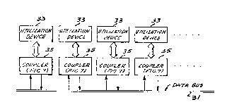
FIGURE 6 illustrates a data communication system formed in
accordance with the invention that includes a data bus 31; and, a plurality of
utilization devices 33, each connected to the data bus by a coupler 35. The binary
data signals flowing between the utili~ation devices and the respective couplersare in rectangular form. Preferably, the data signals are Manchester biphase data
20 signals. Further, preferably the data bus is a current mode data bus formed by a
pair of twisted wires. The couplers 35 convert the binary data to be applied to the
data bus from rectangular form to doublet form. More specifically, preferably the
couplers convert data signals generated by the utilization devices from
rectangular form into a form in which a doublet occurs for each transition of the
25 binary data; and, apply the doublets to the data bus 31. Data signals received by
the couplers are converted by the couplers 35 from doublet form into rectangularform. While FIGURE 6 depicts all couplers as having the ability to both transmitand receive data, it is to be understood that couplers associated with utilization
devices that only transmit or only receive data only require a coupler having the
30 related ability.
A coupler 35 formed in accordance with the invention having the
ability to both transmit and receive data is illustrated in FIGUI~E 7. The transmit
ability is provided by a transmit coupler 37, and the receive ability is provided by
a receive coupler 39.
The transmit coupler 37 is connected to the related utilization
device 33, from which it receives Manchester biphase data signals designated TX0and TXN. More specifically, the transmit coupler includes: a stub driver 41; a
~L3~33
--8--
transmit stub 43, e.g., a shielded pair of wires, which may be up to fifty (503 feet
long; a line driver 45; and, a transmit coupler transformer 47. As will be better
understood from the following description, the stub driver 41 receives the TX0 and
TXN signals and converts them from Manchester biphase form into doublet form
and, via the transmit stub 43, transmits the doublet coded binary signals to theline driver. The line driver 45 amplifies the doublets and applies the amplifiedresult to the data bus via the transmit coupler transformer 47.
The receive coupler 39 receives data signals carried by the data
bus 31 in doublet form, converts the signals into Manchester biphase form and
applies the result, designated RXl and RXN, to the associated utilization device.
I~ore specifically, the receive coupler 39 includes: a receive coupler
transformer 49; a receive amplifier 51; a receive stub 53, e.g., a shielded pair of
wires, which may be up to fifty (50) feet long; and, a stub receive~ 55. The
receive coupler transformer 49 receives the binary data in doublet form carried by
the data bus 31 and applies the doublets to the receive amplifier 51. The receive
amplifier 51 converts the doublets into bipolar pulses, and amplifies the pulses.
The bipolar pulses are applied to the stub receiver 55, which uses the pulses to reconstruct the original Manchester b;phase coded signals as the RXI and RXN
signals.
Both the transmit and receive stubs 43 and 53 are shielded, twisted
wire pairs connected at either ends to low impedances, as described below. This
arrangement allows relatively long stubs to b~- used (up to 50 feet in one actual
embodiment of the invention). In addition to carrying signals, the transmit stub 43
carries power frorn the stub driver 41 to the line driver 45 and the receive stub 53
25 carries power erom the stub receiver 55 to the receiver amplifier 51.
FIGUl~E 8 is a partially block and partially schematic diagram of a
stub driver 41 suitable for use in the transmit coupler illustrated in FIGURE 7.The stub driver illustrated in FIGURE 8 includes: stub driver logic 43; two
resistors designated R1 and R2; two MOSFETs (metal oxide semiconductor field
30 effect transistors) designated Q1 and Q2; two capacitors designated C1 and C2;
and, a transformer designated T1. T1 has two primary windings designated P1 and
P2 and two secondary windings designated S1 and S2. Because T1 functions to
combine two signals in a bipolar manner, the direction oE the primary and
secondary windings of T1 is important. As a result, in accordance with
35 conventional symbology, the direction of the primary and secondary windings of
T1 is denoted in FIGURE ~ by dots located at one end of each wlnding.
As will be better understood from the following discussion of
fi,~.``
F:,
~3~?3 9~3~
g
FIGURE 9, the stub driver logic 43 converts each transition of a Manc~,ester
biphase data signal into a pail of juxtaposed pulses on separate outputs. The
pulses, designated Dl and D2, are juxtapo~sed in the sense that one of the pulses,
Dl, immediately precedes the other pulse, D2. The Dl pulses are applied to the
5 gate terminal of Q1 and the D2 pulses are applied to the gate terminal of Q2. The
gate terminal of Ql is also connected through R1 to a positive voltage source
designated +V1; and the gate terminal of Q2 is also connected through R2 to +V1.The source terminals of ~1 and Q2 are connected to ground. The drain terminal
of Q1 is connected to the dot end of winding Pl of T1 and the drain terminal of Q2
10 is connected to the nondot end of winding P2 of Tl. The dot end of P2 is
connected to the nondot end of P1, and the junction between Pl and P2 is
connected through both C1 and C2 to ground. The junction between P1 and P2 is
also connected to a positive voltage source designated +V2. The dot end of
winding S1 of T1 is connected to one end of one oî the stub wires 43. The nondot15 end of S2 of T2 is connected to one end of the other stub wire. The dot end of S2
is connected to the nondot end of S1 and the junction between S1 and S2 is
connected to +V2.
In operation, D1 and D2 switch Ql and Q2 on and off to create an
amplified current flow through T1 that corresponds to the D1 and D2 pulses. T1
20 converts the Dt and D2 pulses from single polarity form into bipolar form, i.e.,
creates a doublet, DT, from the bipolar pulses. Power for use by the line driver 45
(FIGURE 10) is supplied by +V2 and transmitted to the line driver via Sl and S2,and the transmit stub wires.
As noted above, F[GURE 9 is a block diagram of stub driver logic
25 suitable for use in the stub driver 41 illustrated in FIGURE 8. The stub driver
logic illustrated in FIGURE 9 includes: two four-input AND gates designated G1-
G4; five two-input AND gates designated G5-G9; five two-input OR gates
designated G10-G14; five D flip-flops designated FF1-FF5; and, three inverters
designated 11-13. While the logic illustrated in FIGURE 9 can be embodied in
30 discrete component form, preferably, it is implemented in PAL (ProgralDmable
Array Log~ic) form. In any event, FIGURE 9 and the following logie diagrams all
use conventional negation symbology. In this regard, each of the four-input AND
gates G1-G4 has two negation inputs and both inputs of G7 are negation inputs.
An enable signal denoted TXE is applied to one input of each of G1-
35 G4. TX0 is applied to one input of G1, one of the negation inputs of G2 and one ofthe inputs of each of G5 and G6. TXN is applied to one input of G3, one of the
negation inputs of G4 and one input of each of G8 and G9. The outputs of G1 and
~,~
:13~ 33
-10-
G2 are each connected to one input of GlO; and, the output o~ G1() is connected to
the D input of FFl. The Q output of FFl is applied to one of the negation inputsof Gl, the second negation input of G2, the second input of G5, one of the
negation inputs o~ G7, and one input of G12. The outputs of G5 and G6 are each
5 connected to one input of Gll. The output of Gll is connected to the D input of
FE2. The Q output of ~F2 is connected to the second negation input of C~1, the
follrth input of G2 and the second input of G6.
The outputs of G3 and G4 are each connected to one input of G13, the
output of G13 is connected to the D input of FF3. The Q output of FF3 is
10 connected to one of the negation inputs of G3, the second negation input of G4,
one input of G8, second negation input of G7 and the second input of Gl2. The
outputs of Ga and G9 are each connected to one input of Gl4. The output of G14
is connected to the D input of FF4. The Q output of FF4 is connected to the
second negati~n input of G3, the fourth input of G4 and the second input of G9.
The output of G~ is connected to the input of I1. The signal
previously denoted Dl, and illustrated in FIGURE 8, occurs on the output of I1.
The output of Gl2 is connected to the D input of FF5. The Q output of FF5 is
connected to the input of 12. The output o~ 12 is connected to the input of I3. The
signal denoted D2, and illustrated in FIGURE 8 and previously described, occurs on
20 the output of 13. Clock pulses generated by a suitable clock pulse generator (not
shown), are applied to the clock tCK) inputs of each of FF1, FF2, FF3, FF4 and
FF5.
The lines designated TX0 and TXN of FIGURE 14 is an exemplary
illustration of Manchester biphase data signals of the type whose transition are25 converted by the stub driver logic illustrated in FIGURE 9 into pairs of juxtaposed
Dl and D2 pulses. As shown there, when no Manchester biphase data signals are
present, denoted as the b~ls quiet state, TX0 and TXN are both in the same binary-
state, e.g., they are both low. A data word begins with a sync signal, which takes
up three bit times and forms an "illegal" Manehester code, followed by a series of
30 data bits. I)uring the first half of the sync signal, TX0 changes to the binary state
opposite its bus quiet state i.e., it goes high, while TXN remains in its bus quiet
state. At the midpoint of the sync signal -- the middle of the third bit time, TX0
and TXN both change states, i.e., TX0 shifts ~rom a high state to a low state and
TXN shifts from a low state to a high state. Thus, TX0 and TXN are placed in
35 their biphase states. ~ollowing the sync period, conventional Manchester biphase
codes representing "0" and "1" are produced as determined by the content of the
data word. As depicted in the third and fourth lines of FIGURE 14, D1 and D2
~30~;33
-11-
pulses are produced for each transition of either (or both) TX0 or TXN. Dl, in
essence, is coincident with the transition and D2 immediately follows D1. As
previously discussed, D1 and D2 have the same polarity. Dl and D2 have a pulse
width equal to one clock period, CK. As previously discussed above with respect
5 to FIGURE 8, the D1 and D2 pulses are amplified by Ql and Q2 and converted by
T1 from adjacent pulse form into doublet (DT) form, as shown on the fifth line of
FIGURE 14.
FIGURE 10 is a schematic diagram of a line driver suitable for use in
the transmit coupler illustrated in FIGURE 7. The line driver illustrated in
10 ~IGURE 10 includes two circuits-- a coupling circuit 61 for applying the doublet
signal, DT, to the transmit coupler transformer ~7, and, a power off shorting
circuit 63 for shorting the primary side of the transmit coupler transformer 47 in
the event of a power loss.
The coupling circuit 61 comprises: two resistors designated R3 and
15 R~; a transformer designated T2; four MOSFETs designated Q5, Q6, Q7 and Q8; azener diode designated ZD1; and, three capacitors designated C3, C4 and C5. T2
has two primary windings designated P3 and P4 and four secondary windings
designated S3, S4, S5 and S6. Because the T2 functions as a switch that controlsthe operation of Q5-Q8 in accordance with the state of the doublet signal, the
20 winding direction of both the primary and secondary windings of T2 is important.
As with T1, in accordance with conventional nomenclature, winding direction is
denoted by dots located at one end of each of t~.e windings of T2.
One of the stub wires 43 is connected to the dot end of P3. The
nondot end of P3 is connected to the dot end of P4 and the nondot end of P4 is
25 connected to the other stub wire. Consequently, P3 and P4 are connected in
series. R3 is connected in parallel with P3 and P4. Power for the operation of the
line driver, +V2, is provided at the junction between P3 and P4. The power is
produced by the stub driver 41 and transmitted to the line driver 45 via the
transmit stub 43 in the manner illustrated in FlGURE 8 and described above.
The nondot end of S3 is connected to the gate terminal of Q5. The
drain terminal of Q5 is connected to the junction between P3 and P4 and, thus,
receives +V2 po~Ner. The souree terminal oE 125 is connected to the dot end of S3
and to the drain terminal of Q6. The gate terminal of Q6 is connected to the dotend of SD~. The source terminal of Q6 is connected to the source terminal of Q7.35 The gate terminal of Q7 is connected to the nondot end of Q5. The drain terminal
of Q7 is connected to the source terminal of Q8 and to the nondot end of S6. Thedot end of S6 is eonnected to the gate terminal of Q8. The drain terminal of Q8 is
~3(~3~9~
-12-
also connected to the junction between P3 and P4 and receives +V2 power. The
junction between Q6 and Q7 is connected to the anode of ZD1 and to one side of
C3. The cathode of ZD1 and the other side of C3 is connected to both the nondot
end of S4 and to the dot end of S5. The nondot end of S4 and the dot end of S5 is
also connected through R4 to the junction between P3 and P4, i.e., the +Y2 powersuppl~. C4 and C5 are connected in parallel, between the junetion between P3 andP4, i.e., the +V2 power supply, and ground.
The transmit coupler transformer 47 has three primary windings
designated P5, P6 and P7. Preferably, each of the primary windings is a two turnwinding whereby the turns ratio between each of the primary windings and the
data bus 31 is 2:1. Two of the primary windings, P5 and P6 are connected to the
coupler circuit 61. More specifically, the junction between Q5 and Q6 is
connected to one end of P5. The other end of P5 is connected to one end of P6.
The other end of P6 is connected to the junction between Q7 and Q8. The junctionI 5 between P5 and P6is also connected to ground.
In the absence of a doublet, DT, being applied to the primary
windings, P3 and P4, of T2, QS and Q8 are switched off and Q6 and Q7 are
switched on and short P5 and P6. Q6 and Q7 are chosen to have relatively low
drain to source resistance values-- two ohms each, for example. Because the
turns ratio connecting Q6 and Q7 to the data bus 31 is 4:1 ~2:1 + 2:1) an impedance
value o~ approximately one-fourth of an ohm is applied by windings P5 and P6 to
the current data bus 31 in the absence of a do~blet. Thus, when no data is beingtransmitted, the coupling circuit 61 creates a minimal load on the current mode
data bus 31.
When a doublet, DT, is applied to T2, one of Q5 and Q8 switches on
and one of Q6 and Q7 switches off for the first half of the doublet, followed bythe other one of Q5 and Q8 switching on, and the other one of Q6 and Q7
switching off. As a result9 an amplified doublet is applied to the current mode
data bus 31 via the transmit coupler transformer 47. During the doublet
transmission interval, switching one of Q6 and Q7 off is, of course, necessary to
remove the shorting of P5 and P6 created by Q6 and Q7 during inactive periods.
The power off shorting circuit 63 comprises: two resistors designated
R5 and R6; and, four depletion type JFETs (Junction field effect transistors)
designated Q9, Q10, Qll and Q12. The drain terminals of Q9 and Q10 are
connected to one er.d of the third primary winding, P7, of the transmit coupler
transformer 47. The drain terminals of Q11 and Q12 are connected to the other
end of P7. The gate terminals of Q99 Q10, Qll and Q12 are all connected to
3~
-13-
ground. R5 is connected in series with R6 between +V2 and ground. The source
terminals Q9, Q10, Q11 and Q12 are all connected to the junction between R5 and
R6.
~9, Q10, Q11 and Q12 are all turned off in the presence of +V2
power. If power to the transmit coupler is lost, i.e., +Y2 drops to zero, Q9, Q10,
Q11 and Q12 are all turned on. As a result, Q9, Q10, Q11 and Q12 are all
connected in parallel with P7. Because ~9, Q10, Q11 and Q12 are all connected inparallel, the resistance they apply to P7 is low. This resistance can be loweredfurther by adding more ~FETs in parallel with Q9, Q10, Q11 and Q12. The power
turn off circuit ~3 does not load the transmit coupler transformer 47 when a
doublet is being applied to the current mode data bus 31 by the coupling circuit 61
because, during one swing of the doublet, either Q9 and Q10 or Q11 and Q12 do
not conduct while the other two conduct, and vice versa, during the opposite
polarity swing of the doublet. The nonconducting pair prevent current flow
l S through P7 and, thus, loading by the power off shorting circuit 63.
FIGURE 11 is a schematic dia~ram of a receiver amplifier 51 suitable
for use in the receive coupler 39 illustrated in FIGURE 7. The receiver amplifier
illustrated in FIGURE 11 comprises: a depletion type JFET designated Q13; four
PNP transistors designated Q14, QlS, Q16 and Q17; two NPN transistors
designated Q18 and Q19; four diodes designated DD1, DD2, DD3 and DD4; a zener
diode designated ZD2; three capacitors designated C6, C7 and C8; and, five
resistors designated R79 R~, R9, R10 and R11. ~
The primary winding of the receive coupler transformer 49 is formed
by the current mode data bus 31. The receive coupler transformer 49 has two
secondary windings designated S7 and S8. S7 and S8 are connected in series and
the junction between S7 and S8 is connected through R11 to ground. The other
end of S7 is connected to the source terminal of Q13 and to the emitter of Q14.
The other end of S8 is connected to the drain terminal of Q13 and to the emitterof Q16. The collector of Ql4 is connected to the base of Q18 and to the anode ofDD1. The cathode of DD1 is connected to the anode of DD2. The cathode of DD2
is connected to the base of Q15 and to one end of R7. The other end of R7 is
connected through R8 in series with C6 to the emitters of Q15 and Q18, and
through C8 to ground. The collector o-f Q18 is connected to ground. The collector
Oe Q15 is connected to one of the wires of the stub 53 and the junction between
C6 and R8 is connected to the other wire. The wire connected to the junction
between C6 and R8 carries a signal denoted R~A and the wire conn~cted to the
collector of Q15 carries a signal denoted R~B.
33
-14-
The collector of Qlfi is connected to the base Oe Q19 and to the anode
of DD3. The cathode of DD3 is connected to the anode of DD4 and the cathode of
DD~ is connected to the base of Q17 and to one end of R9. The other end of R9 isconnected through R10 in series with C7 to the emitters of Q17 and Q19 and
5 through C8 to ground. The collector of Q19 is connected to ground. The collector
of Q17 is connected to the same wire of the stub 53 as is the junction between C6
and R8, i.e., the wire that carries the RSA signal. The junction between R10 andG7 is connected to the same wire of the stub 53 as is the collector of Q15, i.e.,
the wire that carries the RSE~ signal. The junction between R7, R8, R9, R10 and
lO C8 is also connected through R1~ to the bases of Q14 and Q16. The bases of Q14
and Q16 are also connected to the anode of ZD2. The cathode of ZD2 is
connected to ground.
The turns ratio between the secondary windings of the receive coupler
transformer 49 is relatively high-- 20:1, for example. As a result, the amount of
15 signal power extracted by the receive coupler transformer from the current mode
data bus 31 is relatively small. A small signal current flowing in the secondarywindings, S7 and S8, of the receive coupler transformer is amplified by low input
impedance, grounded base transistor amplifiers formed by Q14 and Q16 and their
related biasing components. The reverse voltage drop across ZD2 controls the
20 bias voltage on the bases of Q14 and Q16. As a result, the total (quiescent)
collector current flow of Q14 and Q16 does not change with the collector voltagechanges that track doublet current flows through S7 and S8.
Q14 and Q16 in combination with R7 and R9 convert small current
flow changes to relatively high voltage changes. In this regard, in one actual
25 embodiment of the invention, the input impedance values of Q14 and Q16 were 30
ohms and the resistance values of R7 and R8 were 600 ohms. DDl and DD2, and
DD3 and DD4 overcome a dead zone for the emitter follower drivers formed by
Q18 and Q15, and Q19 and Q17, and their related biasing elements. In this regard,
the forward voltage drop of DDl and DD2, and DD3 and DD4, should be chosen to
30 equal the base-emitter voltage drop of Q18 and Q15 and ~19 and Q17,
respectively. Amplification power is provided by the stub receiver 55 illustrated
in FrGURE12 and described below via the receive stub 53. Finally, Q13 is
normally off. If power is lost, Q1 turns on and shorts S7 and S8. As a result, when
power is lost, the load applied by the receive coupler to the current mode data
35 bus 31 is minimized.
FIGURE 12is a schernatic diagram of a stub receiver 55 suitable for
use in the receive coupler 39 illustrated in FIGURE 7 and described above~ The
13~933
-15-
stub receiver 55 illustrated in FIGURE 12 comprises: two NPN transistors
designated Q20 and Q21; a PNP transistor designated Q22; three diodes designatedDD5,DD6, and DD7; a ~ener diode designated ZD3; five capacitors designated C9,
C10, ~11, C12 and C13; twelve resistors designated R13 through R24; two
comparator amplifiers designated OA1 and OA2; and, stub receiver logic 71. Stub
receiver logic is illustrated in FIGURE 13 and described below.
The wire of the stub 53 carrying the R~A signal is connected to the
collector of Q20, through C9 to the inverting input of OA1 and through C11 to the
noninverting input of OA2. The wire of the stub 53 carrying the RSB signal is
connected to the collector of Q21 and through C10 to the noninverting input of
OA1 and the inverting input of OA2. The emitters of Q20 and Q21 are connected
together and through R14 to a negative voltage source designated -V3. The bases
of Q20 and Q21 are connected together, to the collector of Q22 and through R15
to the emitters of Q20 and Q21. The base of Q22is connected through R13 to -V3
and to the cathode of DD5. The anode of D~5 is connected to the anode of ZD3
and the cathode of ZD3 is connected to ground. R16 and R17 are connected in
series across the wires of the stub 53. The junction between R16 and R17 is
connected to the emitter of Q22.
R18, Rl9, R20 and R22 are connected in that order between a
positive voltage source designated +V3 and -V3. The magnitude of +V3 is equal tothe magnitude Oe -V3. The junction between R18 and R19 is connected to the
inverting input of O~1. The junction between R20 and R22is connected to the
noninverting input of OA2. The junction between R19 and R20 is connected
through R22to the noninverting input OI OA1 and the inverting input of OA2. The
output of OA1 is connected to one input of the stub receiver logic 71 and through
C12 in series with R23 to -V3. The junction between C12 and R23is connected to
a latch input of OA1. The latch input of OA1 is also connected to the cathode ofDD6. The anode of DD6 is connected to ground. The output of OA2 is connected
to a second input of the stub receiver logic 71. The output of OA2 is connected
through C13 in series with R24 to -V3. The junction between C13 and R24 is
connected to the latch input of OA2. The latch input OI OA2 is also connected tothe cathode of DD7. The anode of DD7 is connected to ground.
R16 and R17 have equal values and their combined value is equal to
the characteristic resistance of the stub 53. The voltage that powers the receiver
amplifier ~FIGURE 11) is provided by -V3 through ~14, Q20 and Q21. The
magnitude of this voltage is controlled by ZD3 and Q22. Q20 and Q21 and R14
also form a fault sensing CilCUit. More specifically, these components sense an
13~ 33
increase in the current drawn by the receiver amplifier via the wires of the
receive stub 53. (Pault sensing cireuits associated with the line driver 45, thetransmit coupler transformer 47, the receive coupler transformer 49 and the
receiver amplifier 51 can be used to switch a load resistor in parallel with C8 to
5 create an increased current flow to the receiver amplifier to indicate the
presence of a fault.) An increased current drain causes an increased voltage drop
across R14 that can be utilized to actuate a detector to indicate that the data
being reproduced by the receive coupler 39 is potentially erroneous and/or lead to
a shutdown of the receive coupler 39.
In the absence of a doublet, the difference between the RSA and RSB
signal wire voltages is zero. As a result of this zero difference and because the
biasing network formed by Rl8, Rl9, R20 and R21 generates signal threshold
voltages, VTH, at the inputs of OAl and OA2, the outputs of OAl and OA2 are
low. When a doublet occurs, the RSA and RSB differential signal pulses are
15 detected by OAl and OA2 provided that the differential signal amplitude as
coupled to the inputs of the OAl and OA2 by C9, ClO and Cl1 exceeds the signal
threshold, VTH. More specifically, OA1 detects RSB-~SA V~H pulses,
hereinafter called RSA pulses, and OA2 detects RSA-RSB VTH pulses,
hereinafter called RSB pulses. The output pulses are stretched by the latch inputs
20 of OAl and OA2.
In essence, the latch inputs cause the outputs of OAl and OA2 to
remain in a high state for a predetermined per.od of time after the RSA and RSB
doublet created pulses end. The latching time constant is determined by the value
of the OAl and OA2 output circuit components C12,R23 and I)D6, and C13, R24
25 and DD7, respectively. The time is chosen to provide an overlap between the
stretched pulses. Thus, if an RSA pulse occurs before an RSB pulse, the output of
OAl remains high until the output of OA2 shifts high and vice versa if an RSB
pulse occurs before an RSA pulse.
While a single comparator could, of course, be used to detect RSA or
RS~ pulses, dual comparators, i.e., OAl and OA2, are used so that an output is
produced at the earliest possible time after a doublet is detected. Thus,
regardless of the polarity of the first pulse of a doublet, the output of one of OAl
or OA2 will switch states as soon as the earliest pulse of a doublet oceurs.
As noted above, the latch inputs of OA1 and OA2 extend the period of
3S the outputs of OAl and OA2. The purpose of the extension is to further make
certain that the outputs of OAl and OA2 actuate the stub receiver logic. In thisregard, as noted above, the first or second pulses of a doublet are approximately
``` 13(~933
-17-
the width of a clock period. Because RSA and R~B pulses created by a doublet
could be shorter than a clock period, a switch in the states of outputs of OA1 and
OA2 that is only equal to the length of an RSA Dr RSB pulse might not be detected
by the stub receiver logic. Extending the period of the square wave by utilizing5 the latch inputs of OA1 and OA2 prevents this possibility from occurring. A
comparator amplifier used in one embodiment of the invention to form 5~A1 and
OA2 is the LT1016 comparator amplifier produced by Linear Technology, 1630
McCarthy Boulevard, Milpita~ California, 95035.
FIGURE 13 is a block diagram of stub receiver logic 71 suitable for
l0 use in the stub receiver 55 illustrated in FIGURE 12. The stub receiver logicillustrated in FIGURE 13 comprises: four three-input AND gates designated G15,
G16, G17 and G18; ten two-input AND gates designated G19 through G28; two
two-input OR gates designated G29 and G30; two four-input OR gates designated
G31 and G32; five flip-flops designated FF6, FF7, FF8, FF9, and FF10; and, a two15 stage binary counter desi~nated CT1. As with the previously described logic
circuit, the logic circuit illustrated in FIGURE 13 uses conventional negation
symbology. In this regard, G15, G16 and G18 each have two negation inputs. G17,
G23, G24 and G27 each have one negation input.
The output of OA1 (FIGURE 12) is applied to one input of G15, one
20 input of Gl9 and one input of G20. The output of OA2 is applied to one input of
G16, one input Oe G21 and one input of G22. The outputs of G15 and G16 are each
connected to one input of G29. The output of a29 is connected to the D input of
FF6. The Q output ot FF6 is applied to a negation input of G15, a negation inputof G16, the second input of G19 and the second input of G21. The outputs of G19,25 G20, G21 and G22 are each applied to one input of G31. The output of G31 is
applied to the D input of FF7. The Q output of FF7 is applied to the second
negation input of G15, the second negation input of G16, the second input of G20and the second input of G22.
The Q output of FF6 is also applied to one input of G23, the negation
30 input of G24, the negation input of ~:17, the negation input of G18, one input of
G25 and the clear input of CT1. The outputs of G23 and G24 are each connected
to one input of G30. The output of G30 is connected to the D input of FF8. The Qoutput of FFg (RXI) is applied to the negation input of G23, the second input ofG24~, an input of G17, one input of G25 and one input of G26. The outputs of G17,
35 G18, G25s and G26 are each applied to one input of G32. The output of G32 is
connected to the D input of FF7. The Q output of FF7 ~RXN~ is applied to the
second input of G17 and an input of G18.
13~ 33
-18-
~ serial data clock signal denoted RXCK, having a pulse rate equal to
twice the data bit rate and a fixed phase relationship to the received data stream
is applied to the D input of FF10 and one input of G27. The Q output of FF10 is
applied to the negation inpùt of G27. The output of G27 is applied to the data (D)
5 input of CT1 and to one input of G28. The carry (CO) output of CT1 is applied to
the input of G28. The output of G28 is applied to the second negation input of
G18 and to the second input of G2~;.
The stub receivcr logic illustrated in the upper left-hand corner of
FIGURl~ 13, creates a strobe pulse in the clock domain for each doublet. This
l 0 pulse occurs on the output of FF~. In essence, this logic is two channel logic that
responds to which one of OA1 and OA2 first switches its output state from low tohigh in response to doublet created RSA and RSB pulses. If OA1 switches first,
the resulting shift in output of G15 from a lo~ state to a high state is clocked into
FF~ to create a strobe pulse. If OA2 switches first, the resulting shift in the
15 output of G16 from a low state to a high state is clocked into FF6 to create a
strobe pulse. The creation of multiple strobe pulses for a single doublet are
prevented by Gl9, G20 and FF7 in the case of a G15 created strobe pulse and G21,G22 and FF7 in the case of a G16 created strobe pulse. More specifically, the
clock pulse occurring after the output of FF6 shifts Erom low to high clocks the20 high output of FF6 into FF7 if the related OA1 or OA2 output is still high via one
of G19, G20, G21 or G22. ~s a result, FF7 disables G15 and G16 for a clock pulseperiod after a strobe pulse ends.
The portion of the stub receiver logic located on the right side of
FIGURE 13, i.e., FFû and FF9 and the gates associated therewith (G23, G24, G30,
25 G17, G18, G25, G26 and G32), create Manchester biphase data signals identical to
the Manchester biphase data signals that originally produced the doublets that
created the strobe pulses. In this regard, FF8 toggles for each strobe pulse. FF9
follows FF8 and produces the complement of the output of FF8.
The circuit formed by FF10, G27, CT1 and G28 is a special counter
30 circuit that forces the output of RXI and RXN to a bus quiet state in the absence
of strobe pulses. More specifically, RXCK is a timing signal having a
predetermined period. As noted above, the period may equal eight clock pulses
and bear a fixed phase relationship with the received bit stream. RXCK is
reclocked and differentiated by FF10 in combination with 1::2?. While RXCK is a
35 square wave, the OUtpilt of ~27 is a pulse that occurs on the rise of RXCK. The
two stage binary counter, CT1, switches its carry (CV) output state after three
pulses have occurred on the output oî G27. G28, in essence, requires the
~3~33
-19-
production a fourth pulse before its output shifts from a low state to high state.
When the output of G28 switches to a high state, which will only occur if no strobe
pulses have cleared CTl, the output of FF9, RXN, is set to the same state as the- output of FF8. As illustrated in FIGUl~E 14, this state is the bus quiet state that
5 occurs at the end of the RXI and RXN signals.
In summary, the illustrated and described embodiment of the
invention provides a data communication system that transmits data over a
current mode data bus in an efficient and highly reliable manner. The transmit
couplers attached to the data bus produce a relatively high voltage, high
lO frequency output signal. The high voltage allows the invention to be used with a
relatively long data bus, in particular a data bus suitable for use on large
commercial aircraft. Because the frequency of the doublet coded signal is
relatively high, the area and volume of the transmit and receive coupler
transformers can be made relatively low. Thus, the weight of such transformers
15 can be minimized. Further, the circuitry that coacts with the transformers
minimizes the load created by the transmit and receive couplers. The transmit
coupler load is minimized by minimi2ing the resistance "seen" by the bus when
doublets are not being transmitted. This feature has the further advantage of
allowing the receive couplers to receive data doublets while the related
20 transmitter is transmitting. This "listen while talking" feature allows the
utilization devices to recognize and react to transmission clashes, which can occur
when the data communication system is initialiy energized. The load created by
the receive couplers is minimized by minimizing reflected series resistance. In
addition, both the transmit and receive couplers are designed to short their
25 respective transformer windings in the event of a power failure and, thus, avoid
loading the bus if a power failure occurs.
While a preferred embodiment of the invention has been illustrated
and described, it will be appreciated that various changes can be made therein
without departing from the spirit and scope of the invention. For example, while30 the preferred data bus is a current mode data bus, it is to be understood that the
data bus could be some other type of electromagnetic data bus, such as a voltagemode data bus, or an optical mode data bus. Like a current mode data bus, data
communication system, a voltage mode data bus communication system
incorporating the invention, can use small size transformers to couple terminals to
35 the data bus because the doublet signals do not contain low frequency
components. While the transformer size advantages will not be achieved in an
optical mode data bl~s data communication system, because transformer coupling
33
-20-
is not utilized, other advantages are achieved. For example, the amount of energy
applied to the light emitting devices used in such a system to produce high
intensity pulses is less than the amount of energy needed to produce mark-space
signals. As a result, the energy conversion and, thus, the heat generated by the5 light emitting devices is significantly reduced. Because energy conversion andheat generation is reduced, the life of the light emitting devices is increased.Further, the production of pulses coincident with the transitions of mark-space
signals allows the pulses to be utilized to automatically create complementary
signals, such as Manchester biphase data signals in the manner outlined above.
10 Consequently, the invention can be practiced otherwise than as specifically
described herein.