Note: Descriptions are shown in the official language in which they were submitted.
~3~ 587
SPEC I F ICATIO N
TITLE OF THE INVENTION
FU Z Z Y COMPUTERS
BACKGROUND OF THE I2~VENTION
This invention relates to fuzzy computers.
The digital computer was cxeated by harmonizinq the concept
of a stored program, Boolean algebra and the stable operation of
binary hardware, and the comprehensive development of logic and
thorough processing of data have been made possible by the
continuous operation of such a computer. The stable operation
of the digital computer assures high reliability, and digital
computer systems are continuing to grow in scale. A digital
computer is capable of being programmed at will as long as the
program does not contain information on the same mental level as
that of human beings. In this sense, a digital computer is even
referred to as a general-purpose machine. The realization of
digital computer systems is greatly revolutionizing human life
and human society.
The very important concept of "fuzziness" has come about by
considering what and how human beings think and how they
communicate with one another. L.A. Zadeh proposed the concept
of fuzzy sets in 1965. Since then, theoretical studies
~3~ii8~
concerning fuzziness have found their way into print in a large
number of technical papers, but reports on applications are
still few and these have merely relied upon the assistance of
binary digital computers.
Research on fuzziness emphasizes that human knowledge is
based on accummulated experience that is to be generalized in
the form of linguistic information, as is the ~now-how possessed
by specialists. This linguistic information generally possesses
vagueness, obscurity, uncertainty, incompleteness or
impreciseness and is characterized by a membership function.
The grade of membership is expressed by numerical values in the
region of from 0.0 to 1.0 and varies within this range.
When linguistic information is handled by a digital
computer, the grades (values) of membership are represented by
binary codes. The binary-coded values are stored, transferred
and operated on again and again in binary electronic circuits in
accordance with a stored program. As a result, a long period of
time is required to process fuzzy information by a digital
system. Furthermore, the binary-coded values require an
unbelievably large number of elements in order to be stored and
operated upon. Though a digital computer is indeed a general-
purpose machine as mentioned above, it is not necessarily best
suited to the real-time processing of fuzzy information. Thus,
-there is need of another type of machine capable of processing
fuzzy information effectlvely and at high speed.
-- 2 --
~l3~
SUMMARY OF THE INVENTION
An object of the present invention is to provide a hardware
system suitable Eor processing fuzzy information, namely a novel
system referred to as a "fuzzy computer".
According to the present invention, the foregoing object is
attained by providing a fuzzy computer comprising a plurality of
membership function generator circuits each for generating electric
signals, which are distributed on a plurality of lines,
representing a predetermined fuzzy membership function, and a
fuzzy inference engine which receives as inputs the electric
sisnals outputted by the plurality of membership function
generator circuits for executing a predetermined fuzzy operation
and for outputting the result of the operation as electric
signals distributed on a plurality of lines.
The fuzzy membership function is a se-t of function values
tgrades) corresponding to a plurality of variables. In
accordance with the present invention, the plurality of
variables are given concrete form by the plurality of signal
lines, and each value of the fuzzy membership function is
represented by an analog electric signal which appears on each
signal line. That is, the fuzzy membership function is
expressed by electric signals distributed on the plurality of
signal lines.
In a fuzzy computer according to the invention, the analog
signals distributed on the plurality of signal lines
s~
representing a predetermined ~uzzy membership ~unction are
outputted by each of the plurality of fuzzy membership function
generator circuits. The fuzzy inference engine subjects these
analog electric signals to a predetermined operation in their
existing form and also outputs a membership function, which
represents the results of the operation, as a distribution of
electric signals.
Since the fuzzy membership function is not coded into binary
values as is done in a conventional digital computer, the
arithmetic operations are performed at higher speed and
real-time processing is made feasible. In addition, the fuzzy
computer according to the invention has a form most suitable for
fuzzy information processing.
BRIEF DESCRIPTION OF THE DRAWINGS
Fig. 1a is a circuit diagram illustrating an example of an
n-input, l-output MIN circuit, Fig. 1b is a circuit diagram
illustrating an improvement over the circuit of Fig. 1a , and
Fig. 2 is a circuit diagram illustrating an n-input, l-output
MAX circuit.
Figs. 3a through 6 show classes of MIN circuits or MAX
circuits, in which Fig. 3a illustrates the concept of a
corresponding MIN (C-MIN) or corresponding MAX (C-MAX) circuit
and Fig. 3b the symbol thereof; Fig. 4a illus-trates the
concept of an ensemble MIN (E-MIN) or ensemble MAX (E-MAX)
circuit and Fig. ~b the symbol thereof; Fig. sa illustrates
~3~S15 ~
the symbol of a cartesian product (or direct product) MIN
circuit (CP-MIN) and Fig. sb the simplified circuit thereof;
and Fig. 6 is a circuit diagram illustrating a concrete example
of a circuit symbolized as the intersections of lines in Fig.
5b.
Fig. 7 illustrates the concept of a truncation circuit, and
Fig. 8 is a circuit diagram showing a concrete example of a
truncation circuit.
Figs. ga and gb are block diagrams illustrating MIN circuits
and MAX circuits connected in cascade, respectively, Fig~ 10 is
a circuit diagram illustrating a concrete example of the circuit
of Fig. ga and Fig. 11 is a circuit diagram illustxating a
circuit from which compensators in the circuit of Fig. 10 have
been omitted.
Fig. 12 is a circuit diagram illustrating a controlled
MIN-MAX circuit.
Fig. 13 illustrates the concept of a basic fuzzy inference
engine;
Fig. 14 is a block diagram illustrating a fuzzy inference
engine of Type I.
Fig. 15 is a block diagram illustratiny a portion of the
construction of a fuzzy inference engine of Type II, and Fig. 16
is a circuit diagram illustrating a concrete circuit
corresponding thereto.
Fig. 17 is a block diagram illustrating the construction of
-- 5
~2~
a fuzzy inference engine of Type III, and Fig. 18 is a circuit
diagram illustrating a concrete circuit corresponding thereto.
Fig. 19 illustrates the concept of an expanded fuzzy
inference engine, and Fig. 20 is a block diagram illustrating an
example of the construction thereof.
Fig. 21 is a block diagram showing the basic construction of
a fuzzy memory.
Fig. 22 is a circuit diagram illustratlng a fuzzy membership
function generator circuit realized by using a switch matrix,
and Fig. 23 illustrates the concrete construction of a symbol
used in Fig. 22.
Fig. 24 is a circuit diagram illustrating a fuzzy membership
function generator circuit realized by using a pass transistor
array, Fig. 25 illustrates the concrete construction of a symbol
used in Fig. 24, Fig. 26 is a table illustrating the operation
of a decoder in Fig. 24, Fig. 27 is a circuit diagram
illustrating the concrete construction of the same decoder, and
Fig. 28 is a circuit diagram showing a NAND gate used in the
circuit of Fig. 27.
Fig. 29 is a circuit diagram illustrating a voltage
distribution generator circuit capable of selecting the shape of
a fuzzy membership function.
Fig. 30 is a block diagram illustrating an expanded form of
a membership function generator circuit.
Fig. 31 is a block diagram illustrating the concept of a
~02~a~
fuzzy computer.
Fig. 32 is a block diagram illustrating an example of a
parallel processing-type fuzzy computer using basic fuzzy
inference engines.
Fig. 33 is a block diagram illustrating an example of a
parallel processing-type fuzzy computer using expanded fuzzy
inference engines.
Fig. 34 is a block diagram illustrating an example of a
sequential-type fuzzy computer, Fig. 35 is a circuit diagram
illustrating a concxete example of a C-MAX and voltage-holding
circuit in Fig. 34, and Fig. 36 is a time chart illustrating the
operation of switches in Fig. 35.
DETAILED D~SCRIPTION OF THE PREFERRED EMBODIMENTS
1. Fuzzy inferences
Rules based on human experience can be expressed in their
simplest form by the following proposition:
I'If x is A, then y is B."
Here '!if x is A" is referred to as an "antecedent", and "then y
is B" is referred to as a "consequent". If A and B are ltems of
vague linguistic information such as "tall", "old man" and
"positive, small value", then it will be possible to
characterize them by fuzzy membership functions, as mentioned
above. That is, A and B are fuzzy sets. (In a description of
specific circuits given hereinbelow, A, B and the like indicate
fuzzy membership functions or voltage distributions that
,.~ .
represent fuzzy membership functions.)
The abovementioned proposition can be simply expressed as
x = A ~ y = B
Human beings often make inferenees in whieh fuzzy
expressions are included in the antecedent and eonsequent. An
inference of this type can not be satisfactorily implemented using
elassie Boolean logie.
Consider an inferenee of the following form:
Implication: x = A ~ y = B
~Premise: : x = A'
Conclusion : y = B'
This form of inference is referred to as a "generalized
modus ponens", in whieh the eonelusion is inferred from the
given premise when an implieation exists.
A large number of implieation rules ean exist, as follows:
Implieation 1: x = Al --~ y = Bl else or and
Implication 2: x = A2 ~ ~ Y = B2 else or and
.
.
Implication r: x = Ar ~ Y = Br
Premise : x = A'
Conclusion : y = B'
A large number of implications are connected by "else" or
~3~2~
"and".
There is also an inference of the following form:
Implication: x = A ---~ y = B
Premise: : x = B'
Conclusion : y = A'
This form of inference is referred to as a "generalized
modus tollens''O
Basically, a fuzzy computer is composed of a fuzzy memory
storing the abovementioned implication rules and a fuzzy
inference engine which implements modus ponens-type fuzzy
inferences (see Fig. 31).
A further analysis of a modus ponens fuzzy inference will
now be given.
We wlll consider the concept of a "fuzzy relation from A to
B", which is expressed by RAB t referred to simply as R).
In general, when the following holds:
A = {al, a2, ..., ai, ..., am}
B = {b1, b2, ..., bj~ ..., bn}
a fuzzy relation R from A to B is expressed as follows:
rll rl2 - - rl j . . . rln
r21
R = .
ri,l ri
: .
rml ' rmn
~L3¢~2~
Various operations representing this fuzzy xelation have
been proposed. For the details, see Masaharu Mizumoto and
Hans-Jurgen Zimmermann, "Comparison of Fuzzy Reasoning Methods",
Fuzzy Sets and Systems, Vol. 8, No. 3, pp. 253 - 283 (1982).
An example of a typical fuzzy relation already proposed is
as follows:
rij = ai ~ bj MIN Operation Rule
... (1)
ij (ai ~ bj) V (1 - ai) MAX Rule
ri~ ai A bj) Arithmetic Rule
The MIN operation rule expressed by Eq. (1) is the best
known and its effectiveness in industrial applications has been
demonstrated. In the present embodiment, therefore, the
operation rule of Eq. (1) is employed. However, it goes without
sayin~ that the other operation rules are applicable as well.
When the premise (x = A') is given for one implication rule
(x = A > y = B), as mentioned above, a "compositional rule of
inference" for a case where the conclusion (y = B') is inferred
from the above is expressed as follows using the fuzzy relation
R:
B' = A' ~ R
- [al ~ a2 ~ ai~ ... , am']
rll ..... rln
, rij ~
rml ..... rmn
-- 10 --
~3~
= [bl', b2', ..., bj, ..., bn']
Various operations have also been proposed for the operation
* in the above equation. For example, there are those using a
MIN/MAX operation, an algebraic product/MAX operation, etc. In
the present embodiment, the MIN/MAX operation, which is used
most commonly, is employed as the operation ~.
Accordingly, if the MIN/MAX operation is used as the ~
operation and the Eq. (1) is used as the fuzzy relation, the
conclusion bj based on the compositional rule of inference is
expressed as follows:
bj~ = (al' A ri j ) \/ ( a2 ~\ 2 j
V (ai ~ ri~ V (am' ~ r j)
= V ai ~ rij (2)
~n
= ~Vl ai l\ ( ai A bj)
m
= V ai A ai ~ b
/\ ( \/ ai A ai ) ( 4
~- ~ . . .
The operations of these Eqs. ( 2 ), ( 3) and (4)are executed by
the fuzzy inference engine constituting the principal part of
the fuzzy computer, as mentioned above. It will be appreciated
from these equations that the fuzzy inference englne is
primarily constituted by ~IN circults and MAX circuits.
Before discussing the construction of the fuzzy inference
engine, therefore, the ~IN circuit, ~IAX circuit and other basic
5~
circuits will be described. Though voltage signals and current
signals may serve as analog electric signals that indicate the
values (grades) of membership functions, the following
discussion will take a circuit that operates in a vol-tage mode
as an example.
2. MIN circuits, MAX circuits and other basic circuits
(1) MIN circuits, MAX clrcuits
Fig. 1a illustrates an example of an n-input, l-output MIN
circuit constructed using bipolar transistors. The circuit
executes the operation z =~ xi, where the input voltages are xl,
x2,... xn and the output voltage is z. In other words, the
circuit generates an output voltage equal to the smallest input
voltage.
This MIN circuit is composed of a comparator and
compensator. The comparator is constituted by n number of PNP
rs Qll' Q12' Q13 ~ Qln connected together at their
emitters, and a transistor Ql serving as a current source for
driving these transistors. The input voltages xl - xn are
applied to the bases of the transistors Qll ~ Qln~ respectively.
A reference voltage ~1 is impressed upon the base of transistor
Q1 in such a manner that a predetermined constant current Il
will flow into the transistor Ql Since the transistor among
the transistors Qll ~ Qln that has the lowest input voltage
(represented by Vmin) impressed upon its base is rendered
conductive, the other transistors assume the cut-off state.
5~
Accordingly, a voltage obtained by adding the emitter-base
voltage VEB of the transistor rendered conductive to this input
voltage Vmin, namely a voltage Vmin + VEB ~xi VE3 ( EB
the order of 0.7 V), appears at the emitters. If two input
voltages are equal in value and lower than the other input
voltages, a current of Il/2 will flow into each of the
transistors to which these two input voltages are applied. The
results, therefore, are the same. The same will be true if
three or more of the input voltages are equal and lower than the
other input voltages.
The compensator is for the purpose of compensating the
voltage VEB that appears as a MIN operation error at the output
of the comparator. The compensator is composed of an NPN
transistor Q2 and a transistor Q3 serving as a current source
for driving the transistor Q2. A voltage ~2 necessary for a
constant current I2 to flow is applied to the base of the
transistor Q3. The emitter of transistor Q2 is connected to the
output terminal of the MIN circuit. The result of subtracting
the base-emitter voltage VBE of transistor Q2 from the
comparator output voltage is that the output voltage z is
expressed by ~xi.
The transistors Ql' Q3 serving as current sources can be
substituted by resistors. Also, one PNP transistor having its
emitter connected to the power supply Vcc can be provided, in
which case this transistor and the transistor Ql would form a
- 13 -
~L3~2~
current mirror. It can also be arranged so that a desired
current Il will flow by adjusting a resistor connected in series
with this newly provided transistor.
Fig. 1b illustrates an improved MIN circuit, in which
elements similar to those shown in Fig. 1a are designated by
like reference characters.
In the MIN circuit of Fig. 1a, the VEB's of transistors
Qll ~ Qln are not necessarily of the same value. However, let
the emitter-base voltage be VEBi provisionally, considering
transistor Qli as being representative. Let the VBE of
transistor Q2 be VBE2. Full compensation of the error in the
MIN operation by means of the compensator takes place when
VEBi = VBE2. That is, assuming that the transistors Qll ~ Qln
and Q2 have exactly the same VEB - IE (or V~E - IE)
characteristic, the error will be O when Il - I2 holds. In
order to establish the relationship Il = I2 with the circuit of
Fig. l(a), the voltages ~ 2 must be adjusted.
In the improved circuit of Fig. 1b, a transistor Q~ is
provided in series with the transistor Q2~ and the transistors
Q4 and Ql construct a current mirrorO If a constant current I2
is passed through the transistor Q2~ a current Il satisfying the
condition Il = I2 will flow into the transistor Ql~ so that no
adjustment of the voltages ~ 2 is required. Further, if a
transistor Q5 is provided to construct a current mirror with the
transistor Q3 serving as the current source and the transistor Q5
~L3~58~
is driven by a current source Io~ then I2 = Io will hold at all
times. In other words, a constant current is capable of flowing
at all times irrespective of any fluctuation in the power supply
voltages Vcc, -VEE. Such a circuit will be highly resistant to
power supply fluctuations. Drive can be achieved by the single
current source Io by constructing a current mirror using the
transistor Q5 and a transistor Q6 serving as a current source of
another MIN circuit.
Though this improvement is effective when an extremely rigid
operation is considered, no practical problems are encountered
even if the currents Il, I2 are different, as will be set forth
later in a discussion of a controlled MIN-MAX circuit.
Fig. 2 shows an example of a MAX circuit. The ~AX circuit
is also composed of a comparator and compensator. The
comparator is constituted by emitter~connected NPN transistors
Q21' Q22' ~ Q2n whose bases are controlled by input voltages
xl, x2, ..., xn, respectively, and a transistor Q7 for driving
these transistors. Only the transistor among the transistors
Q21 ~ Q2n that has the highest input voltage ~represented by
Vmax) impressed is rendered conductive, so that a voltage
equivalent to Vmax - VBE appears at the emitters. The error in
-VBE is compensated by the compensator, which comprises a PNP
transistor Q9 and a transistor Q8 serving as a current source.
As a result, an output voltage z equivalent to Vmax = V xn
appears at the output terminal. It goes without saying that
~3~12~il~'7
this L~AX circuit can be improved in accordance with the approach
illustrated in Fig. 1b.
In these MIN and MAX circuits, the input voltages x~
represent fuzzy truth values ~each value (grade) of a membershlp
function]. Fuzzy truth values are continuous values [0,1] of
from O to l. In correspondence with this, the input voltages
are set at e.g. [OV, 5V].
Since all of the transistors in the above-described MIN and
MAX circuits are connected together at their emitters, these
circuits are named "emitter-coupled fuzzy logic gates" (ECFL
gates).
The above-described MIN and MIX circuits can be considered
as two cascade-connected emitter followers driven by the current
sources (transistors Ql' Q3' Q7' Q8~ Accordingly, these
circuits exhibit a very high input impedence and a very low
output impedence. This fact indicates that these circuits are
highly resistant to external noise and exhibit little
cross-tal~. This means that a number of circuits can be
connected in succeeding stages.
Since the aforementioned MIN and MAX circuits are driven by
current sources, the transistors do not saturate. In other
words, an effect in which minority carriers are stored in the
base region does not occur. Accordingly, these circuits exhibit
a very high processing speed. Tests have shown that speed of
response is less than 10 nsec.
- 16 -
~3~2~;il37
Furthermore, the input/output static characteristics of the
overall circuits are not affected even if one or several of the
input terminals of the circuits are opened. This is very
important for constructing a large-scale system.
The PNP and NPN transistors in the above-described circuits
can be substituted by p-channel and n-channel MOSFETs,
respecti~ely.
The foregoing facts apply not only to the aforementioned MIN
and MAX circuits but also to all of the circuits mentioned
hereinbelow.
(2) Classes of MIN and MAX circuits
Expanded forms of MIN and MAX circuits will now be
considered, and these will be classified into several forms for
the sa~e of describing circuits that construct a fuzzy inference
engine.
In order to consider solely the two inputs xl, x2 in the MIN
circuit of Fig. 1, the transistors Q13 ~ Qln for the other
inputs will be deleted. In addition, the inputs xl, x2 will be
replaced by x, y. By so doing, the MIN circuit of Fig. 1 is
rendered into a 2-input, l-output MIN circuit which performs the
operation z = x ~ y. If n-number of these 2-input, l-output MIN
circuits are prepared, the result is a 2n-input (xl, x2, ....
n' Yl~ Y2~ Yn)~ n-output (Zl~ Z2~ ~ Zn) MIN circuit, as
shown in Fig. 3a. In this circuit, one output Zi is obtained
as Zi = Xi ~ Yi depending upon the corresponding inputs xi, Yi.
~3~125~37
Accordingly, this type of MIN circuit shall be referred to as a
"corresponding MIN circuit" (abbreviated to "C-MIN"). Likewise,
a 2n-input, n-output IYAX circuit for performing a MAX operation
Zi = Xi ~ Yi (i = l - n) shall be referred to as a
"corresponding MAX circuit" (abbreviated to "C-MAX").
C-MIN, C--~AX can be symbolized as shown in Fig. 3b. The
bold arrows which resemble the well-~nown symbols for bus lines
represent n-number of signal lines. The character "n" written
inside the arrows indicates the number of signal lines. Each of
the n values of the membership functions X, Y is represented as
a voltage distributed on each signal line. ~herefore, it can be
said that C-MIN, C-MAX are circuits for respectively executing
the MIN and MAX operations of the two membership functions X, Y.
Voltages representing n values of a membership function Z
produced as a result of executing the operation also appear as
distribution on n signal lines.
In contrast to the above-described C-MIN and C-MAX circuits,
the n-input, l-output MIN and MAX circuits shown ln Figs. 1a or 1b and
2 output the results of an ensemble ope~ation performed on n
input signals and for this reason shall be referred to as an
"ensemble MIN circuit" and an "ensemble MAX circuit"
(abbreviated to "E-MIN" and "E-MAX", respectively). These
circuits are illustrated in simplified form in Fig. 4a and are
symbolized as shown in Fig. 4b.
One more special MIN circuit will now be proposed. This is
- 18 -
~2~
a cartesian product (or direct product) MIN circuit (referred to
as a "cartesian product MIN circuit" or "CP-MIN") which executes
the above-described "fuzzy relation from A to s". In the
present embodiment, as indicated by Eq. (1), the ~IN operation
rule is employed as the operation which represents the fuzzy
relation.
This CP-MIN is a circuit to which the inputs are
A = {al, a2, ..., ai, ..., am}
B = {bl, b2, ..., bj~ ..., bn}
and which outputs the fuzzy relation
R = [rl, r2, ..., rj, .--, rn]
rlj
r
r j -
r
mj
ij i ~ j - ~ `
The symbol of the CP-MIN is as shown in Fig. 5a, and the
simplified circuit is as depicted in Fig. 5b. Fig. 6
illustrates a concrete example of a circuit symbolized as the
intersections of lines ai, bj and rij in Fi~. 5b. The circuit
of Fig. 6 is a MIN circuit modified to have two inputs by
deleting the transistors Q13 ~ Qln of the MIN circuit in Fig. la.
In Fig. 6, elements corresponding to those shown in Fig. la are
-- 19 --
~.3(~258~
designated by like reference charaeters.
(3) Truncation circuits
As shown in Fig. 7, a truncation eireuit euts off an
inputted membership function X at a certain value a and outputs
a membership funetion X' obtained as a result of the eut-off
operation. As will be illustrated later, this circuit is used
to construct a fuzzy inference engine using MIN and MAX
operations. The truneation circuit has n inputs, the single
truncating input a, and n outputs.
A speeifie example of a truneation eireuit is depieted in
Fig. 8. The n inputs representing the fuzzy membership function
X are xl, x2, ..., xn, and the truneated output ~uzzy membership
funetion X' is represented by xl', x2', ..., xn'. It can be
said that this circuit is obtained by providing n-number of
2-input, l-output MIN cireuits (i.e. C-MINs) in parallel and
connecting one input of each MIN to the corresponding inputs of
the other MINs to form the truncating input a. The eircuit can
also be said to eomprise a truneator and a eompensator.
(4) MIN-MAX circuits, MAX-MIN circuits
A cascade connection of a MIN circuit and a MAX circuit is
often used in order to construct a ~uzzy inference engine,
described later. Figs. 9a,9b,illustrate examples of such a cascade
conneetion. In Fig. 9a, the output sides of an m-input E-MIN
and an n-input E-~IN are eonneeted to the input side of a
2-input MAX circuit. Fig. 9b illustrates a eircuit obtained
- 20 -
~.3~258~
by connecting a 2-input MIN circuit to the last stages of an
m-input E-MAX and n-input E-.~AX. Examples of cascade
connections between a MIN circuit and MAX circuit are not
limited to these. Other examples which can be conceived of
include a cascade connection between a C-MIN and E-MAX, a
connection among a plurality of E-MINs provided in parallel
and an E-MAX, etc.
A concrete example of the circuit shown in Fig. ga
obtained by utilizing~the specific MIN and MAX circuits shown in
Figs. la and 2 is illustrated in Fig. 10. The characters
shown in Figs. la and 2 are adopted as the characters of the
elements constituting one E-MIN and the MAX circuit. However,
the character Qlm is assigned to the transistor Qln. The
characters indicating the corresponding elements of the other
E-MIN have the prime symbol ""' assigned thereto. The
transistor corresponding to the transistor Qlm is assigned the
character Qln'
The compensator (transistor Q2) of the ~-MIN shown in Fig.
10 compensates for a positive voltage shift at the emitter
junction of the comparator, as mentioned above. The compensator
(transistor Qg) in the 2-input MAX circuit compensates for a
negative voltage shift at the emitter junction of the comparator
in the preceding stage. Since the compensator of the E-MIN and
the compensator of the MAX circuit compensate for voltage shifts
in mutually opposing directions, the value of the final output z
- 21 -
~ . .,
~3~ 37
will not change even if these compensators are omitted.
Fig. 11 illustrates a circuit which results by deleting the
two compensators in accordance with the above approach. It will
be appreciated that the circuit of Fig. 11 is much simpler in
comparison with that of Fig. 10. Thus, transistors can be
conserved, a higher operating speed can be attained and
power consumption can be reduced. It goes without saying that
this technique of omitting the compensators can be used
effectively in a cascade connection between a MAX circuit and
NIN circuit or in a cascade connection between a truncation
circuit and MAX circuit.
(5) Controlled MIN-MAX circuits
A controlled MIN-MAX circuit acts as a MIN circuit or MAX
circuit, depending upon the control input. An example is shown
in Fig. 12. The circuit possesses two signal inputs x, y, one
control input c and one output z.
The circuit illustrated in Fig. 12 is obtained by deleting
Q12 Qlm~ Q12 Qln in the E MIN of the
MIN-MAX circuit shown in Fig. llo The signal inputs x, y are
pplied to the bases of transistors Q11' Qll .
controlled by the control input c is connected between the
emitters of the transistors Qll~ Qll' The analog switch
comprises an n-channel MOSFET Q31 and a p channel M3SF~T Q32
connected in parallel. The control input c is connected to the
gate of the FET Q31 directly and to the gate of the FET Q32 upon
- 2~ -
.~,
,,
25;~
being inverted by an inverter.
The control input c is a binary signal, namely a signal
which takes on an H level (e.g. 5 V) and an L level (e.g. O V).
If the control input c is at the L level, the analog switch is
turned off. In this case, the circuit 12 is precisely the same
as a circuit that would be obtained by eliminating the
12 Qlm~ Q12 Qln from the circuit of Fig 11
Therefore, an output equivalent to z = (~x) V (~y) = x V y is
obtained and the circuit acts as a MAX circuit. (Though ~ x, ~y
are equal to x, y and are meaningless as operations, they are
expressed in this fashion as far as an analogy with respect to
Fig. 11 is concerned.) If the control input c is at the H
level, the analog switch is turned on so that the transistors
Q11' Qll' act as comparators and one of the transistors Q21~ Q22
acts as a compensator. Accordingly, the circuit functions as a
MIN circuit [compare this with the circuit shown in Fig. la].
Since the two current sources Ql~ Ql' are present in this case,
addition currents from the two current sources Ql' Ql' flow into
whichever of -the transistors Q11' Q11' is in the conductive
state. In consequence, a voltage shift at the emitter junction
of the transistor rendered conductive will increase slightly and
the compensation performed by the compensator will develop some
error. However, the error poses almost no problem in practical
use. The reason for this is that the VEB-IE characteristic of
the transistor has an extremely steep leading edge. Experiments
~31~ 7
have shown that V~B is 0.71V for an emitter curren-t of 5mA and
0.725 V for an emitter current of 10 mA. Accordingly, even if
the emitter current IE should double, the difference that will
appear in VEB will be only 0.015 V. If the signal input x or y
varies over the range 0 - 5 V (corresponding to fuzzy truth
values of 0 - 1), the value of 0.015 V is entirely negligible.
3. Fuzzy inference engines
(1) Basic inference engines
Discussed next will be a fuzzy inference engine, which is a
unit for implementing the above-described modus ponens fuzzy
inference. Described first will be a basic inference engine
which implements a simple inference, namely one in which the
antecedent of the implication includes only one fuzzy
proposition (the aforementioned "if x is A", i.e. "x = A").
This will be followed by a discussion of an expanded fuzzy
inference engine for implementing more complicated inferences.
The concept of a basic fuzzy inference engine for
implementing simple inferences is shown in Fig. 13. The inputs
to this inference engine are fuzzy membership functions A, B and
A' corresponding to fuzzy propositions given on the basis of the
aforementioned fuzzy inference compositional rule. The
inference engine outputs a fuzzy membership function B'
representing the conclusion. These fuzzy member functions A, B,
A' and B' are implemented by analog voltages distributed on m or
n signal lines which correspond to the elements of the fuzzy
- 24 -
sets~
A basic fuzzy inference engine is a circuit which executes
the operation of Eq. (2), (3) or (4) set forth above. Since at
least three types of fuzzy inference engine arrangements can be
considered to correspond to the Eqs. (2), (3) and (4), these
will be referred to as Type I, Type II and Type III.
(2) Type I
A basic fuzzy inference engine of Type I executes the
operation of Eq. (2). A block diagram thereof is shown in Fig.
1~. A voltage input representing the fuzzy membership function
A and distributed on m signal lines, and a voltage input
representing the fuæzy membership function B and distributed on
n signal lines are applied to a CP-MIN 11, where (n x m) output
voltage signals (rj, j = 1 - n) representing a fuzzy relation R
from A to B are obtained. Also provided are n C-MINs 12 to each
one of which are applied signals (a set of m voltage signals)
representing the fuzzy membership function A', and a signal rj
(rj comprises n voltage signals) representing the results of the
abovementioned CP-MIN operations. The output of each C-MIN 12
comprises m voltage signals representing ai ~ rij (i = 1 - n).
Further provided are n E-MAX circuits 13 each one of which
performs a MAX operation on the m voltage signals inputted
thereto. Accordingly, it is possible to obtain the fuzzy
membership function B' representing a conclusion as a set of
analog voltages bj' distributed on n output signal lines of the
- 25 -
~3~2~
n E-MAXs 13.
It is possible to delete the compensators in the cascade
connection between the C-MINs 12 and E MAXs 13, as described
earller.
(3) Type II
A basic fuzzy inference engine of Type II executes the
operation of Eq. (3). A partial block diagram thereof
is shown in Fig. 15. It is necessary to execute the operation
ai' ~ ai ~ bj (i = 1 - m) for all j's (j = 1 - n).
Consequently, m E-MINs 21 are provided for each value of j, and
bj, ai' and ai (i = 1 - m) voltage signals are inputted to each
E-MIN 21. A total of n x m E-MINs are required. For each value
of j, m outputs of the m E-MINs 21 are delivered to an E-MAX 22.
The E-MAX circuits 22 provided are n in number, and an output
voltage bj' (j = l - n) is obtained from each E-MAX 22.
The compensators can be deleted in the cascade connection
between the E-MINs 21 and E-MAXs 22 in this circuit.
Fig. 16 illustrates a detailed circuit construction o~ part
of the block diagram of Fig. 15 for obtaining one bj
(specifically, bl'). In the E-MINS 21 and E-MAX 22, elements
similar to those shown in Figs. 1a and 2 are designated by
like reference characters and the construction thereof therefore
can be readily understood. A multi-output current mirror is
constructed by the transistors Ql acting as current sources in
E-MINs 21, and a newly provided transistor Q33. The transistor
- 26 -
~3~i8~7
Q33 is driven by current source Ill. Accordingly, all of the
E~MINs 21 are driven by equal currents through a simple
construction. In a similar manner, the transistor Q7 serving as
the current source in E-MAX 22 constructs a current mirror with
a newly provided transistor Q34 and is driven by current source
I12 .
(4) Type III
A basic fuzzy inference engine of Type III executes the
operation of Eq. (4). A block diagram thereof is shown in Fig.
17. Voltages representing the fuzzy membership functions A, A'
and each distributed on m signal lines are applied to a C-MIN
31, where the l~IN operation ai' ~ ai (i = 1 - m) is parformed.
The C-MIN 31 produces m output voltages which are inputted to an
E-MAX 32. The output of the E-MAX 32 represents Vai' ~ ai and
is applied to a truncation circuit 33 as a truncating input a.
A voltage (bj, j = 1 - n) representing the membership function B
and distributed on n signal lines is inputted to the truncation
circuit 33. Ultimately, the truncation circuit 33 performs the
operation of Eq. (4) so that the conclusion B' can be obtained
as a set of analog voltages Bj' distributed on n output lines.
A concrete electronic circuit of the fuzzy inference engine
of Type III is illustrated in Fig. 18. Elements corresponding
to those shown in Figs. la, 2, 8 and 16 are designated by like
reference characters. Compensators are deleted from the cascade
connection between the C-MIN 31 and E-MAX 32. The truncation
- 27 -
~L3~;~5~7
circuit 33 is exactly the same as that shown in Fig. 8. The
transistors Ql' which serve as the m current sources of the
C-MIN 31, together with the transistors Ql ~ truncation circuit
33 and the transistor Q33, constructs a multi-output current
mirror. The transistor Q7 serving as the current source in the
E-MAX 32, together with the transistors Q3 of truncation circuit
33 and a transistor Q34, constructs a multi-output current
mlrror.
The inference engine of Type III is much simpler in
construction than the inference engines of Types I and II.
The inference engine of Type III will consist of
(4m ~ 5n + l)-number of transistors except for transistors Q33, Q34.
In an-experlment using discrete bipolar transistors and not a
monolithic integrated circuit, an operation speed of 100 nsec
(10 7 sec) was obtained. This means that this basic inference
engine is capable of actually implementing 10,000,000 fuzzy
in~erences per second ti.e. 10 megaFIPS, where "FIPS" refers to
fuzzy inferences per second).
(5) Expanded inference engines
There are times when an inference in which the antecedent of
an implication includes two fuzzy propositions becomes
necessary, as will be described next. This is referred to as an
"expanded fuzzy inference". The antecedents of an implication
are connected by "and/or". Either "and" or "or" is selected.
Implication: If x is A and/or y is B, then z is C
- 28 -
~3~2~17
Premise: : x is A' and/or y is B'
Conclusion : z is Cl
This is expressed by symbols as follows:
Implication: x - A and/or y = B > z = C
Premise : x = A' and/or y = B'
Conclusion : z = C'
This expanded fuzzy inference is implimented by an expanded
fuzzy inference engine. The concept of an expanded inference
engine is illustrated in Fig. 19. The inputs are fuzzy
membership func~ions A, B, C, A' and B', as well as a
conjunction selection c for selecting the conjunction "and/or".
The output is a fuzzy membership function C' representing the
conclusion. The fuzzy membership functions A, A' are
represented by respective voltages distributed on m signal lines
each, the fuzzy membership functions B, B' are represented by
respective voltages di-stributed on m' signal lines each, and the
fuzzy membership functions C is represented by a voltage
distributed on n signal lines.
Fig. 20 illustrates the construction of an expanded
inference engine. This is obtained by revising somewhat the
construction of the basic inference engine of Type III shown in
Fig. 17. A C-MIN operation (C-MIN 31A) is performed between the
membership functions A and A', and an E-MAX operation (E-MAX
- 2~ -
~3~12~7
32A) on m voltages representing the results of the C-MIN
operation is executed. C-MIN and E-L~AX operations (C-MIN 31B,
E-MAX 32B) are also performed with regard to the fuzzy
membership functions B, B'. In the present embodiment, the
conjunction "and" is realized by a MIN operation, and the
conjuction "or" is realized by a MAX operation. The
above-described controlled MIN-MAX circuit 34 is used in such a
manner that the conjunction operation and the selection of the
conjuction can readily be performed. The results of the two
E-MAX operations are inputted to the controlled MIN-MAX circuit
34. A conjunction selection input signal c for selecting "and"
or "or" is applied as the control input of the controlled
MIN-MAX circuit 34. The membership function C is applied to the
truncation circuit 33, and the output a of the controlled
MIN-MAX circuit 34 is applied to the truncation circuit 33 as
the truncating signal, A voltage distribution o a fuzzy
membership function representing the conclusion C' is obtained
from the truncation circuit 33.
4. Fuzzy memories
(l) Concept of a fuzzy memory
The function of a fuzzy memory is to store fuzzy membership
functions and to output a designated fuzzy membership function
as a voltage distribution on a plurality of signal lines.
The basic concept of a fuzzy memory which stores a plurality
of fuzzy membership functions and from which these functions are
- 30 -
~3~
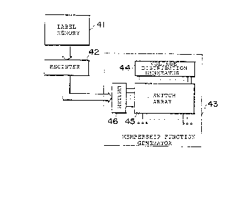
read out is illustrated in Fig. 21. A fuzzy memory is composed
of a label memory 41 storing the labels of fuzzy membership
functions, a register 42 storing codes representing labels read
out of the label memory 41, and a membership function generator
circuit 43 which, by fuzzifying a label, outputs a voltage
distribution corresponding to the label. A label may be thought
of as being a word representing a fuzzy membership function.
The label memory 41 and register 42 are binary devices. The
label memory 41 is e.g. a binary RAM.
The membership function generator circuit 43 is constituted
by a voltage distribution generator circuit 44 for generating a
predetermined voltage distribution on a plurality of signal
lines, a switch array 45 for sending the generated voltage
distribution out on predetermined output signal lines, and a
decoder 46 for controlling the switches of the switch array 45
by decoding a code representing a label read out of the label
memory 41. Though the shape of the vol-tage distribution
generated by -the voltage distribution generator circuit 44 is
predetermined, the position of the voltage distribution on the
output signal lines is changed by the switch array 45 controlled
by the output of the decoder 46. Accordingly, a voltage
distribution representing a fuzzy membership function
corresponding to the label read out of the label memory 41
appears on the output lines.
The fuzzy memory stores the labels of fuzzy membership
~3~25;~37
functions and not the grades (the individual function values) of
fuzzy membership functions converted into a number of binary
codes. This means that the binary memory (memory ~1) need have
only a small capacity. For example, if the number of types of fuzzy
membership functions to be stored is less than eight, then
the labels thereof may be expressed by 3-bit codes and, hence,
one fuzzy membership function can be stored in the form of three
bits. Futhermore, since the access time of an ordinary binary
memory is much shorter in comparison with an anolog memory,
high-speed read-out is possible. Moreover, a fuzzy membership
function expressed by an analog voltage distribution eventually
can be obtained. Since data are stored in the form of binary
codes, the memory is strongly noise-resistant.
Concrete examples of some fuzzy membership function
generator circuits are described hereinbelow. Seven types of
fuzzy membership functions are generated herein. The labels of
these membership functions shall be NL, NM, NS, ZR, PS, PM and
PL. These express the following items of linguistic
information: negative large, negative medium, negative small,
zero, positive small, positive medium and positive large.
Further, the number of points (corresponding to the number of
elements of a fuzzy set) in the region of the variables of a
fuzzy membership function shall be limited to 25. Accordingly,
the output terminals of the fuzzy membership function generator
circuit are 25 in number.
- 32 -
~3~ 7
(2) Fuzzy membership function generator circuit using
a switch matrix
F'igs. 22 and 23 illustrate an example of a fuzzy membership
function generator circuit using a switch matrix as the s~itch
array. In Fig. 22, the fuzzy membership function generator
circuit has output terminals numbered from O to 24, and the
seven types of fuzzy membership functions outputted by these
output terminals are shown below themv
The values of the outputted fuzzy membership functions are
quantized at four levels for the sake of simplicity. For
example, these four levels correspond to voltages of 0, 1.7, 3.3
and 5.0 V. These four levels are decided by a voltage
distribution generator circuit 44A. The latter is provided with
three fuzzy truth value voltage sorces 44a, 44b and 44c for the
three voltages 1.7, 3.3 and 5.0, respectively. Five voltage
lines VL indicated by the slanting lines in Fig. 22 extend from
the circuit 44A. The centrally located voltage line is
connected to the voltage source 44c, the voltage lines located both
sides thereof are connected to the voltage source 44b, and the
two outermost voltage lines are connected to the voltage source
44a.
A decoder 46A is a l-of-8 decoder. A 3-bit (cl, c~, C3)
binary signal representing a label provided by the register 42
is inputted to the decoder 46A~ The decoder 46A outputs an
H-level signal on whichever of the eight output terminals is
- 33 -
~31~ 8~
decided by the code indicated by t~e binary signal. The eight
output terminals correspond to "undecided" and the seven types
of labels. For example, the H-level signal is outputted at the
"undecided" terminal when the input code signal is 000 and at
the NL output terminal when the input code signal is 001.
Signal lines SL indicated by the horizontal lines in Fig. 22
extend from these output terminals with the exception of the
"undecided" output terminal.
Output lines OL are led out to the 25 output terminals from
predetermined intersections of the voltage lines VL and signal
lines SL in the switch matrix 45A. As shown in Fig. 23, a symbol
45a indicated by a small square a-t each of these intersectlons
is a switch, which is constituted by e.g. a MOSFET, provided
between the voltage line VL and output line OL and on/off
controlled by the voltage on signal line SL. It is of course
permissible to provide one output line OL with two or more of
the switches 45a. All of the output lines OL are grounded via a
resistor 45b on the output terminal side.
When a label of a certain fuzzy membership function is read
out of the level memory 41 and applied to the decoder 46A via
the register 42 in the above arrangement, an H-level signal
appears on whichever of the signal lines SL corresponds ko this
label and the switches 45a provided on this signal line are
turned on (closed). As a result, the voltages from the voltage
distribution generator circuit 44A pass through the switches 45a
~3~ 7
which have turned on and appear at the corresponding output
terminals via the output lines OL^ Accordingly, a voltage
distribution representing the abovementioned fuzzy membership
function is outputted.
(3) Fuzzy membership function generator circuit using a
pass transistor array
Figs. 24 and 25 illustrate a fuzzy membership function
generator circuit using a pass transistor array 45B as the switch
array.
A voltage distributor generator circuit 44B is equipped with
ten voltage sources for generating fuzzy truth value voltages
0.0, 0.5, ..., 4.5 and 5.0 V in order to quantize a membership
function at 11 levels. These voltage sources correspond to
fuzzy truth values of 0, 1/10, ..., 9/10 and 1, xespectively.
The generator circuit 44B has a PROM in which the values of a
membership function having the label ZR are programmed. The
PROM has power supply lines VL connected to the abovementioned
voltage sources and ground, and output llnes OL connected to
output termianls via the pass transistor array 45~. The PROM
comprises two aluminum layers arranged one on the other. The
output lines OL are formed on the first layer and the power
supply lines VL on the second layer. These two layers are
insulated from each other by an insulative layer consisting of
e.g. photosensitive polyimide. The shape of a fuzzy membership
function is programmed by forming through-holes at points of
intersection of these layers. Since the through~holes can be
formed by a mas~ ROM technique, a membership function having any
shape can be programmed. The black circles depicting the nodes
of the lines VL and lines Ol. indicate the through-holes. The
lines VL are connected to the lines OL at the points where the
through-holes are formed and it is at these points that the fuzzy
truth value voltages are transferred to the pass transistor
array 45B. It is permissible for the node of two lines VL and
OL to be shorted by a field ROM technique, namely by causing
insulative breakdown of the desired cross point by application
of a high voltage.
The pass transistor array 45B comprises the output lines OL
led out from the voltage distribution generator circuit 44B, the
signal lines SL connected to the seven terminals of the decoder
46B, slanting lines BL for shifting the voltages at the
intersections of the lines OL, SL four or eight digits to the
left or right, and switching elements, namely PMOSFETs, 45c
provided at respective ones of the intersections of the signal
lines SL, and output lines OL and slanting lines sL and controlled
by the voltages on the respective signal lines SL. The manner
in which the switching elements 45c are connected is illustrated
in Fig. 25. The seven signal lines SL connected to the decoder
46B or -the rows of switching elements controlled by these lines
shall be designated Sl, S2, ..., S7. S1 - S7 will also refer to
the signals on these lines SL where appropriate.
- 36 -
~3~3125~
The switch row Sl shifts a membership function, which has
been programmed in the voltage distribution generator circuit
44~, four digits to the left, the switch rows S3, S~ and S6
shift the membership function four digits to the right, eight
digits to the left and eight digits to the right, respectively.
The switch rows S2 and S5 are for delivering the programmed
membership function directly to the output terminals and do not
shift the function to the left or right. The switch array S7 is
a grounded switch array. When the switches S7 are on and the
other switches Sl - S6 are off, all of the output terminals are
dropped to ground level.
Fig. 26 illustrates the relationship between the labels of
fuzzy membership functions and the binary levels of the signals
Sl - S7. The decoder 46B converts the 3-bit binary signals cl,
c2, C3 (O V or +5 V) from the register 42 into the 7-bit binary
signals Sl S7 [-5 V (L level) or +5 V (H level)] in accordance
with the table shown in Fig. 26. The decoder 46B is composed of
a combination of NAND gates 47 and inverters 48, as shown in
~ig.27.
By way of example, the switch rows S3 and S6 turn on if the
label outputted by the label memory 41 is PL. The membership
function programmed in the voltage distribution generator
circuit 44B is shifted four digits to the right through the
switch row S3 and is shifted eight digits farther to the right
through the switch row S6. As a result, ~he programmed
- 37 -
,. . .
~L3~5l~
membership function is shifted 12 digits to the right and the
membership function which appears at the output terminals is PL
(positive large).
In Fig. 24, 25 centrally located output lines OL are
connected to the line VL of the voltage distribution generator
circuit 44B that is connected to ground level. ~lso connected
to this line -~L are 24 (12 x 2) lines located on the right and left of
the central output lines OL and lying parallel thereto, as well
as the slanting lines`BL. Switch element rows Sl, S2, S3, S4,
S5 and S6 are provided at the points where these lines intersect
the signal lines SL. This arrangement is for the
purpose of assuring that ground-level signals will be outputted
to the output terminals regardless of how the programmed
membership function is shifted.
The pass transistor array 45B must pass the fuzzy truth
values (0 - 5 V) to the output terminals without attenuation.
When a fuzzy truth value voltage is lower than the threshold
voltage of a PMOSFET in an ordinary PMOS circuit, the PMOSFET
will not attain the fully conductive state if the gate voltage
VG (decoder output) is O V. In order for the PMOSFET to be
turned on rully, lt is required that VG be made - 5V. To
accomplish this, the decoder 46~ is adapted to generate outputs
which take on values of -5 V (L) and +5 V (H), as mentioned
above. Fig. 28 illustrates an example of the N~ND gate 47
constituting the decoder of Fig. 27 for generating these output
- 38 -
~3~ ii87
signals Sl - S7.
(4) Selection of fuzzy membership function shape
The ~uzzy membership functions illustrated in the foregoing
description are chevron or triangular in shape. However, a
variety of membership functions are conceivable and it would be
desirable to be able to select different shapes depending upon
need.
Fig. 29 illustrates a voltage distribution generator circuit
applicable mainly to a fuzzy membership function generator
circuit of the type shown in Fig. 22 and adapted to enable
selection of the shape of a fuzzy membership function. The
OUtp~lt lines VL connected to several voltage sources 44a - 44d
are provided with output lines OLl connected so as to output a
voltage distribution representing a chevron- or triangle-shaped
fuzzy membership ~unction, and output lines OL2 connected so as
to output a voltage distribution representing a function having
a trapezoidal shape. A switching element or NMOSFET 40A is
connected to each line OLl, and a switching element or NMOSFET
40B is connected to each line OL2. The lines OLl, OL2 are
connected to the output lines OL, which are connected to the
output terminals, on the output sides of these switching
elements. The switching elements 40B are directly controlled by
a selection signal c~, and the switching elements 40A are
controlled by the signal cO applied via an inverter 49.
When the selection signal cO is at the L level, the
- 39 -
~s ~3ql~Z37
switching elements 40A turn on and voltages representing a
chevron- or triangle-shaped fuzzy membership function are
outputted on the output lines OL. Conversely, if the signal cO
is at the H level, the elements 40B turn on so that voltages
representing a function having a trapezoidal shape are
outputted. Thus, it is possible to select the shape of the
fuzzy membership function.
In the circuit of Fig. 29, let the threshold value voltage
of the FETs 40A, 40B be VTH (usually 1 V). In such case, it
will suffice if tbe L level of the binary selection signal cO
controlling these FETs is less than VTH and the H level is above
VTH + 5 V. Here the value of 5 V is the voltage of the voltage
source 44d that generates the largest voltage.
The shapes of the generated voltage distribution in the
voltage distribution generator circuit, namely the shapes of the
membership functions, are not limited to the aforementioned two
shapes. It is possible to adopt an arrangement in which three
or more shapes can be prepared in advance and any one thereof
can be selected. In addition, it goes without saying that the
selection of function shape is applicable to the fuzzy
membership function generator circuit shown in Fig. 24.
(5) Expanded form of a membership function generator
circuit
A voltage distribution generator circuit generates voltage
signals distributed on a plurality of lines. Accordingly, it is
- 40 -
513~
possible to apply the output voltages of one voltage
distribution generator circuit to a plurality of switch arrays.
Fig. 30 illustrates a membership function generator circuit
which includes one voltage distribution generator circuit 44 and
a plurality of switch arrays 45 to which the output voltages of
-the generator circuit 44 are applied. Each switch array 45 is
driven by a respective decoder 46. Code signals of the same or
different labels are applied to respective ones of the decoders
46. Accordingly, voltage distributions representing a plurality
of the same or different fuzzy membership functions can be
obtained from the membership function generator circuit.
5. Fuzzy computers
(1) Concept of a Euzzy computer
Fig. 31 illustrates the concept of a fuzzy computer. This
fuzzy computer is capable of implementing fuzzy information
processing of the simplest type, or in other words, is applied
to cases where one implication exists. The fuzzy computer
basically comprises a fuzzy memory 54 and a fuzzy inference
engine 50, as mentioned above. Three membership function
generator circuits (hereinafter referred to as MFGs) 43 are
provided in order to generate voltage distributions representing
three fuzzy membership functions A, B and A'. Labels read out
of a label memory 41 and temporarily stored in registers 42 are
applied to the MFGs 43. The three MFGs 43 can be considered to
the same as that shown in Fig. 30, or each MFG 43 can be
- 41 -
;~
~3~l2~
considered to possess its own voltage distribution generator.
The fuzzy membership functions A, B, A' outputted by the fuzzy
memory 54 are applied to the basic fuzzy inference engine 50,
which has been described earlier with reference to Figs. 13
through 18. A fuzzy inference result B' is obtained as
distributed analog voltages, namely in the form of a fuzzy
output. Depending upon the particular case, as in a fuzzy
control system, for example, there are times when it is required
to obtain a definite result, namely a non-fuzzy output, from a
fuzzy computer. An auxiliary defuzzifier 52 e~ecutes such
processing and provides a discrete analog voltage (non-fuzzy
output).
In the fuzzy computer of Fig. 31 and in all of the fuzzy
computers of the types described hereinbelow, the control unit
and control bus for synchronizing computer operation are not
shown.
All of the fuzzy memories described above store the labels
of a plurality of fuzzy membership functions in a binary memory
in advance, and in accordance with the label read out of the
fuzzy mernory, the MFG generates a voltage distribution
representing the corresponding fuzzy membership function.
However, the fuzzy memory or MFG used in a fuzzy computer is not
limited to the type mentioned. It will suffice if the fuzzy
memory and MFG are capable of providing the fuzzy inference
engine with a voltage distribution representing a predetermined
- 42 -
fuzzy membership function. Therefore, by way of example, a
number of voltage distribution generator circuits inclusive of a
PROM of the kind shown in Fig. 24 can be prepared, and these
circuits can be pre-programmed to have different or the same
fuzzy membership functions. Then, in accordance with a
membership function designation input corresponding to a label,
a voltage distribution generator circuit which generates a
designated membership function can be selected, and this output
voltage distribution can be applied to a fuzzy inference engine.
A selection switch array different from that described above
would be necessary in order to apply the output vol-tage of the
selected voltage distribution generator circuit to the fuzzy
inference engine.
(2) Parallel processiny type I
As mentioned earlier, a number of implication rules
generally exist and these are connected by "else or also" or
"and". A concrete example of a fuzzy computer of the type which
simultaneously executes a plurality of fuzzy inferences for a
plurality of implications on the premise that a plurality of
implication rules exist will now be described.
As shown in Fig. 32, r-number of basic fuzzy inference
engines 50 are provided on the premise that r-number of
implication rules exist. A 2~FG 43A is provided for each of the
inference engines 50 in order to generate two membership
functions Ak, Bk tk = 1 - r) in each implication and apply the
- 43 -
~L3~2~8~
membership functions to the inference engines 50. Each 2MFG 43A
includes a combination of two MFGs in a single block. Since -the
fuzzy membership function A' in the premise is common for all of
the fuzzy inference engines 50, one MFG 43 is provided in order
to generate the function A'. This output voltage distribution
is applied to all of the inference engines 50.
Shift registers 42a, 42b are provided in order to apply the
labels of the membership functions Ak, Bk to each 2~FG 43A. The
shift registers 42a are r in number and are connected in series.
The binary data stored in each register 42a are applied to the
corresponding 2MFG 43A in parallel fashion. By way of example,
assuming that a label is expressed as three bits, each shift
register 42a wil be a 3-bit shift register, so that the r shift
registers 42a can be constituted by a (3 x r)-bit shift
register. A label is set in each of the registers 42a by
inputting serial data representing r labels. This is done first
by serially inputting an Ar label code from the label input
terminal of function A, then inputting an Ar 1 label code from
this input terminal, and so on. The foregoing description also
holds for the registers 42b. As for a register 42c, it will
suffice to serially input a 3-bit label representing A'.
Accordingly, with the fuzzy computer shown in Fig. 32, a label
memory is unnecessary. It will suffice to input each label by
means of an input unit such as a keyboard.
When labels have been set in all of the registers 42a - 42c,
- 44 -
~3~25~
all of the 2MFGs 43A and the MFG 43 provide the fuzzy in~erence
engines SO with voltage distributions representing the
corresponding fuzzy membership functions. Accordingly, the
results of the inferences, e.g. s1', s2', ..., Br', are obtained
from respective ones of the inference engines 50.
If the connective of a plurality of implications is given by
"else or also", the connective is implemented by e.g. a C-MAX
53. The connective "and" is implemented by e.g. a C-MIN. Thus,
an analog voltage distribution representing the final conclusion
B' is obtained from the C-MAX 53.
A fuzzy computer of this type would be used to hold a
plurality of implications fixed and successively change the
fuzzy membership function A' of the premise, thereby obtaining
the corresponding conclusions B'. Naturally, it is permissible
to change the implication, depending upon the particular case.
It can be arranged for the labels of A, A' and B to be
applied not only manually from an input unit but also by using
an already existing binary microprocessor.
If the MFG 43 and 2MFGS 43A possess a function which enables
selection of the shape of a generated fuzzy membership function,
as described above with reference to Fig. 29 or 30, one bit of
data will be required. In such case, the registers 42a - 42c
would have to be 4-bit shift registers.
(3) Parallel processing type II
Fig. 33 illustrates a fuzzy computer using expanded fuzzy
- 45 -
~3~2~
inference engines described earlier with reference to Figs. 19
and 20. This fuzzy computer also is of the parallel processing
type capable of simultaneously implementing a plurality of
inferences premised on a plurality of implication rules.
As already described, the inputs which an expanded fuzzy
inference engine 51 requires are three fuzzy membership
functions Ak, Bk, Ck (k = 1 - r) in an implication, membership
functions A', B' in a premise, and a selection signal c for the
conjunction "and/or" of an antecedent in an implication. A
3MFG' 43C is provided for each inference engine 51 in order to
generate volta~e distributions representing the membership
functions Ak, Bk, Ck. Each 3MFG' comprises three MFG's
represented as a single block. The prime symbol ""' means that
the voltage distribution generator circuit 44 is omitted from
the MFG. In other words, the MFG' comprises a decoder and a
switch array, as shown in Fig. 30. Since the membership
functions A', B' are common to all inference engines 51, one
2MFG' 43B is provided in order to generate these functions. The
output voltage of the voltage distribution generator circuit 44
is commonly applied to the 3MFG's 43C and 2MFG' 43B. The 3MFG's
43C and 2MFG' 43s are provided with labels rrom the correspond-
ing registers 42B, 42A. The register 42C outputs the
conjunction selection signal c, which is applied to all of the
fuzzy inference engines 51.
The labels of a number of membership functions are inputted
- 46 -
~3~12~i~37
from an input unit 55 and are stored in the label memory 41 in
advance. The memory 41 is accessed by a control unit, not
shown, whereby predetermined labels are read out of the label
memory 41 successively and are transferred to the registers 42A,
42s. Data representing the conjunction selection are also
transferred to the register 42C. Thus, the 2MFG' 43B and 3MFG's
43C generate voltage distributions representing the
corresponding membership functions, and these voltage
distributions are applied to the inference engines 51. In
consequence, the inference results C1', C2', ..., Cr' are
obtained from the respective inference engines 51. These
results are applied to the C-MAX 53, from which the final result
C' is obtained. If necessary, the fuzzy output C' is converted
into a non-fuzzy output by a defuzzifier 52.
t4) Sequential type
A sequential-type fuzzy computer is for implementing fuzzy
inferences sequentially. Voltage distributions representing
the sequentially obtained inference results are successively
operated on and accumulated in accordance with the connection
operation (MAX or MIN) of plural implications, and the
accumulated results which prevail when all inferences end are
the final results. Alternatively, final results are obtained by
accumulating each of the inference results individually and then
finally subjecting all of the inference results to a connection
operation.
- 47 -
~3i~2~
Fig. 34 illustrates the general features of such a
sequential-type ~uzzy computer. For the sake of slmplicity, a
basic fuzzy inference engine is used. Employed as this engine
is the Type III fuzzy inference engine (see Fig. 17) described
above. This fuzzy computer performs a connection operation each
time inference results are obtained.
It is assumed that there are r implications and that the
fuzzy membership functions in these implications are Ak, Bk (k =
1 - r). It is assumed that the labels of these membership
functions are previously stored in each of the label memories
41A/ 41B in the order in which the inferences are implemented,
e g in the order Al, A2, ..., Ak, ..., Ar 1 2 k
..., Br. The addresses of the locations at which these labels
are stored are designated by a program counter 61.
First, the labels Al, Bl are read out of the respective
memories 41A, 41B, and the membership functions Al, Bl
corresponding thereto are read out of the MFG's 43D and applied
to the C-MIN 31 and truncation circuit 33. Also, the membership
function A' of the premise is applied to the C-MIN 31. As a
result, the inference result Bl' is obtained from the truncation
circuit 33 and stored temporarily in a voltage holding circult
63 via the C-MAX (or C-MIN) 53. Next, in response to
incrementing of the program counter 61, the labels of the next
membership functions A2, B2 are read out of the memories 41A,
41B and these functions are applied to the fuzzy inference
- 4~ -
~l3tg~25X~I~
engine. Hence, the inference result B2' is obtained and applied
to the C-MAX 53. The C-MAX 53 also is provided by the circuit
63 with the immediately preceding inference result B1' and
therefore performs the operation B1' V B2' (the result of this
operation is represented by ~ Bk' for convenience). This ~Bk' is
stored in the circuit 63.
The inference results B3', ..., Bk' are successively
obtained in the same manner and the MAX operation is applied to
these inference results and the immediately preceding inference
results ~Bk', ..., V Bk'. The results of these operations are
stored in the circuit 63.
When the last inference result Br' is finally obtained, the
MAX operation is applied to Br' and ~Bk' to acquire the final
result B' = VBk. This is stored temporarily in a voltage
holding circuit 62. The above-described circuit operation would
be carried out by providing gate circuits between the C-MAX 53
and circuit 63 and between the C-MAX 53 and circuit 62 and
controlling the opening and closing of these gate circuits.
Fig. 35 shows a concrete example of the C-MAX 53, voltage holding
circuits 62, 63 and the aforementioned gate circuits. The
truncation circuit is one from which the compensator is deleted.
That is, this is the truncator of Fig. 8 and is designated by
numeral 33a. Accordingly, the output of the truncation circuit
33a is that obtained by adding the emitter-base voltage VEB to
the inference result Bk'. When the truncation circuit 33a
- 49 -
~ ~25~
outputs a voltage higher than the charging voltage of a
capacitor 65, a diode 64 allows this voltage signal to pass and
charge the capacitor 65, thereby acting as a l~AX circuit. The
diode 64 also acts to compensate for the abovementioned error
VE~ by dropping the forward voltage. The capacitor 65
corresponds to the voltage holding circuit 63, and a capacitor
67 corresponds to the voltage holding circuit 62. Switches SWl,
SW2, SW3 are provided as the aforementioned gate circuits.
These switches naturally are constituted by FETs or the like.
The on/off action of these switches SW1 - SW3 is illustrated in
Fig. 36, in which 1, 2, 3, ..., k, ..., r represent the order
of the inferences.
Before a series of inferences are implemented r times, the
switch SW3 turns on in pulsed fashion, whereby the preceding
result B' accumulated in the capacitor 65 is transferred to the
capacitor 67 via a buffer amplifier 66. The voltage of
capacitor 67 appears at the output terminal at all times through
a buffer amplifier 68. These buffer amplifiers 66, 68 would be
constructed using e.g. high-input impedance MOS input-type
operational amplifiers. All of the charge in capacitor 65 i5
discharged by temporarily turning on the switch SW2.
When a first inference based on the fuzzy membership
functions Al, Bl ends, the switch SWl turns on for a brief
instant, whereby a voltage distribution repre~enting the
inference result Bl is transferred to the capacitor 65. When
- 50 -
~3~25~
the second inference ends, the switch SWl turns on in similar
fashion. The voltage representing the second inference result
s2' is sent to the capacitor 65 only if this voltage is higher.
The MAX operation is performed and the results accumulated. The
above-described circuit operation is repeated at the end of each
inference. When the implementation of the r inferences
end and the switch SWl closes, the final inference
result B', which is the result of the MAX operation applied to
the results of all inferences, is accumulated in the capacitor
65.
As many apparently widely different embodiments of the
present invention can be made without departing from the spirit
and scope thereof, it is to be understood that the invention is
not limited to the specific embodiments -thereof except as
defined in the appended claims.
- 51