Note: Descriptions are shown in the official language in which they were submitted.
~3~t3~
PHOTOVOLTAIC ELEMENT WITH A SEMICONDUCTOR LAYER
COMPRISING NON-SINGLE CRYSTAL MATERIAL CONTAINING
AT LEAST Zn, Se AND H IN AN ~IOUNT OF 1 TO 40 ATOMIC %
FIELD OF THE INVENTION
The present invention relates to an improved photo-
voltaic element which is usable as a power source for
electric appliances and also as a power generator. More
particularly, it is concerned with an improved photovoltaic
element with PN junction which exhibits a high photoelectric
conversion efficiency,particularly for short-wavelength
light.
BACKGROUND OF THE INVENTION
There have been proposed a variety of photovoltaic
elements for solar cells and for power sources in electric
appliances. They utilize the pn junction formed by ion
implantation or thermal diffusion of impurities into a
substrate of single crystal of silicon (Si) or gallium
'3 ~
13U319~
arsenide (GaAs), or by epitaxial growth of an impurity-doped
layer on a substrate o~ such single crystal. ~owever, there
is a disadvantage for these photovoltaic elements that their
production cost unavoidably becomes costly because of using
a single crystal substrate. Because of this, they have not
yet gained general acceptance for use as solar cell or as
power source in electric appliances.
Recently, there has been proposed a photovoltaic ele-
ment in which there is utilized a pin junction of amorphous
silicon (hereinafter referred to as "A-Si") deposited film
formed on an inexpensive substrate of non-single crystal
material such as glass, metal, ceramics, and synthetic resin
by way of the glow discharge decomposition method. This
photovoltaic element has a nearly satisfactory performance
and is of low production cost and because of this, it has
been recognized as usable as a power source for some kinds of
appliances such as electronic calculators and wrist watches.
However, for this photovoltaic element, there is a
disadvantage that the output voltage is low because the band
gap of the A-Si film constituting the element is 1.7 eV,
which is not large enough. There is ano~her disadvantage
that its photoelectric conversion efficiency is low for a
light source such as fluorescent light which contains more
short-wavelength light, so that its application is limited
to appliances with very small power consumption.
;, - 2 -
~ . ,
:135~3~'3~
There is a further disadvantage for said photovoltaic
element that the constituent A-Si film is often affected by the
so-called Staebler-Wronski effect, in which the film
characteristics are deteriorated upon continuous irradiation
with intense light for a long period of time.
For a photovoltaic element to be utilized as a power
supplying solar cell, it is necessary to convert efficiently and
continuously the light energy of sunlight into electric energy,
and hence, it is desired to have such a layer structure that
permits photoelectric conversion for sunlight over as broad a
spectrum range as possible.
Now, in the case where a photovoltaic element is made
of a semiconductor material having a small band energy gap, the
wavelength region of light to be absorbed by the layer will be
extended from the short-wavelength side to the long wavelength
side. However, in this case, it is the long wavelength
component of sunlight alone that contributes to photoelectric
conversion, and the energy of the short-wavelength component is
not utilized for photoelectric conversion. This is because the
amount of energy to be taken out by the photoelectric conversion
is determined by the energy band gap of the semiconductor
material as used.
On the other hand, in the case where a photovoltaic
element is made of a semiconductor material with a large band
energy gap, the wavelength component which is absorbed by the
layer and contributes to photoelectric conversion is the short
w~velength light having an energy greater than the band gap
3~
energy of the semiconductor material and the long-wavelength
component is not utilized for photoelectric conversion.
In a photovoltaic element, the maximum voltage or open-
circuit voltage (Voc) to be supplied is determined by the band
gap energy of the semiconductor materials utilized. In order
to obtain a high Voc, semiconductor materials having a large
band gap energy are desirable.
~ herefore, there is eventually a limit for the
photoelectric conversion efficiency for a photovoltaic element,
which is prepared by using a single semiconductor material.
The foregoing led to an idea of forming a plurality of
photovcltaic elements using a plurality of semiconductor
materials each having a different band gap energy, so that the
individual photovoltaic elements become responsible for
utilizing the different wavelength regions of sunlight. This
idea was expected to contribute to an improvement in the
photoelectric conversion efficiency.
However, there is a disadvantage for the solar cell
having such a structure as mentioned above in that overall high
photoelectric conversion is possible only in the case where the
individual photovoltaic elements have good characteristics,
because it is of such structure that a plurality of photovoltaic
elements are stacked to form an electrically serial structure.
Unfortunately, for the photovoltaic element having the
foregoing structure, there has not yet realized any desirable
one wherein the respective constituent elements as stacked have
satisfactory values of band gap energy and satisfactory
-- 4 --
,. ..
~3tJ31~
characteristics as desired and provides a high Voc as the
photovoltaic element.
There have been proposed direct transition-type
semiconductor films having a wide band gap, such as ZnSe (having
a band gap of 2.67 eV) and ZnTe (having a band gap of 2.26 eV)
and mixed crystals thereof ZnSelxTex (where O < x < 1). Public
attention has been focused on these semiconductor films. These
semiconductor films are, in general, formed on a substrate of
single crystal by way of epitaxial growth. The as-grown film
of ZnSe exhibits n-type conductivity and the as-grown film of
ZnTe exhibits p-type conductivity. However, for any of these
films, it is generally recognized that it is difficult for the
film to exhibit opposite type conductivity. Further, in order
to carry out the epitaxial grown for the film formation, it is
required to use a specific substrate of single crystal and to
maintain the...............................................
13~ 3~
substrate at elevated temperature. And in this film
formation, the deposition rate is low. ~ecause of this, it
is impossible to perform epitaxial growth on a commercially
available substrate which is inexpensive and low heat-
resistant such as glass and synthetic resin. These factors
make it difficult to develop practically applicable semi-
conductors films using the foregoing commercially available
substrates.
Even in the case where a semiconductor film should be
fortunately formed on such commercially available substrate,
the film will be such that is usable only in very limited
applications.
In fact, there have been various proposals to form a
direct transition-type semiconductor film on a non-single
crystal substrate such as glass, metal, ceramics and
synthetic resin. However, under any of such proposals, it
is difficult to obtain a desired direct transition-type
semiconductor film having satisfactory electrical
characteristics because the resulting film is
accompanied with defects of various kinds which make the
film poor in electrical characteristics and on account of
this, it is difficult for the film to be controlled by
doping it with an impurity.
In the meantime,an amorphous film composed of Zn and Se
elements is described in U.S. Patent No. 4,~17,374 (called
13(~3~'3~
"literature 1" hereinafter) and also in U.S. Patent No.
4,226,898 (called "literature 2" hereinafter). And ZnSe
compound is described in Japanese Patent Laid-open No.
189649/1986 (called "literature 3" hereinafter) and Japanese
Patent Laid-open No. 189650/1986 (called "literature 4"
hereinafter).
Now, literature 1 discloses amorphous semiconductor
films containing selenium (se), zinc (Zn), hydrogen (H) and
lithium (Li); but the principal subject is in amorphous selenium
semiconductor films, and the Zn described therein is merely an
additive as is Li and H. And as for the Zn and the Li, likewise
in the case of the H, they are used aiming at reduction of the
localized state density in the band gap energy without changing
the inherent characteristics of the film. In other words, the
addition of Zn to the amorphous Se film mentioned in literature
1 is not intended to positively form a ZnSe compound.
Incidentally, literature 1 mentions nothing about the ZnSe
compound and the formation of ZnSe crystal grains. Regarding
the addition of Li, it should be noted that it is not added as
a dopant.
Literature 2 does mention amorphous semiconductor films
containing Se, Zn, and H. However, it deals mainly with
amorphous silicon, and it defines Se as an element which forms
a compound with said silicon. As for the Zn, it is defined as
an element which sensitizes the photoconductivity and reduces
the localized state density in the energy`gap. In other words,
the additions of Zn and Se are not intended to form a ZnSe
-- 7
~*~,~
x~
~3~
compound. Incidentally, literature 2 mentions nothing about the
ZnSe compound and the formation of the ZnSe crystal grains.
Literature 3 and literature 4 are concerned with the
deposition of a ZnSe film by the HR-CVD method (hydrogen radical
assisted CVD method). That is, they disclose methods of
improving the deposition rate and the productivity of a
deposited film; but they merely mention deposited films of non-
doped ZnSe.
Against this background, there is an increased social
demand to provide an inexpensive photovoltaic element having a
high photoelectric conversion efficiency, particularly, for
shore-wavelength light which may be practically usable as a
solar cell and also as a power source in various electric
appliances.
SUMMARY OF THE INVENTION
The present invention is aimed at solving the
aforementioned problems relating to photovoltaic elements for
use in solar cells and other appliances and satisfying the
foregoing social demand.
It is therefore an object of the present invention to
provide an improved photovoltaic element usable in devices
typified by a solar cell having an improved functional deposited
film which may be desirably formed even on a commercially
available inexpensive non-single crystal substrate of glass,
-- 8 --
. ~,~
~3~J3~'3~
metal, ceramics or synthetic resin and which may form an pn
~unction with another film formed on such substrate,
Another object of the present invention is to provide
an improved photovoltaic element with a pn junction which
provides a high photoelectric conversion particularly for short-
wavelength light and which is usable in devices typified by a
solar cell.
BRIEF DESCRIPTION OF THE DRAWINGS
Figs. l(A) and l~B) are schematic representations
showing the typical layer structure of the photovoltaic element
of the present invention.
Fig. l(C) is a schematic representation shouing the
layer structure of a photovoltaic element prepared in a
Comparative Example.
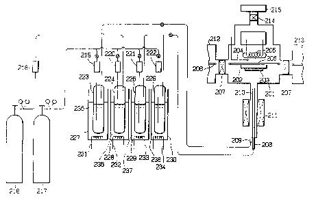
Fig. 2 is a schematic diagram showing the apparatus for
forming a deposited film according to process ~1) of the present
invention.
Fig. 3 is a schematic diagram showing the apparatus for
forming a deposited film according to process (2) of the present
invention.
Fig. 4 is a schematic diagram showing the apparatus for
forming a deposited film according to process (3) of the pres~nt
invention.
Fig. 5 is a graph showing the relation between the
ratio of crystal grain domains and the content of hydrogen (H)
in films formed in Experiments A(2) and A(3).
_ g _
13~31~
Fig. 6 is a graph showing the relation between the
content of hydrogen and the change in conductivity of the films
formed in Experiment B.
Fig. 7 is a graph showing the relation ~etween the
content of hydrogen and the drift mobility of holes in films
formed in Experiment B.
Fig. 8 is a graph showing the relation between the
content of hydrogen and the dark conductivity of films formed
in Experiment C.
Fig. 9 is a graph showing the relation between the
content of hydrogen and the ratio of crystal grain domains in
films formed in Experiment C.
Fig. 10 is a graph showing the relation between the
dark conductivity and the flow rate of hydrogen gas at the time
of film formation in Experiment C.
Fig. 11 is a graph showing the relation between the
content of hydrogen and the ratio of crystal grain domains in
films formed in Experiments D(2) and D(3).
Fig. 12 is a graph showing the relation between the
content of hydrogen and the change in conductivity of films
formed in Experiment E.
Fig. 13 is a graph showing the relation between the
content of hydrogen and the drift mobility of holes in films
formed in Experiment E.
Fig. ~4 is a graph showing the relation between the
contént of hydrogen and the dark conducitvity of films formed
in Experime~t F.
-- 10 --
;~ ."
13U;~.'3~
Fig. 15 is a graph showing the relation between the
content of hydrogen and the ratio of crystal grain domains in
films formed in Experiment F.
Fig. 16 is a graph showing the relation between the
hydrogen content and the dark conductivity in Experiment F.
Fig. 17 is a graph showing the relation between the
content of hydrogen in p-type doped films and the dark
conductivity of films formed in Experiment G with the Se/Te
ratio being a parameter.
Fig. 18 is a graph showing the relation between the
Se/Te ratio in p-type doped films and the dark conductivity of
films formed in Experiment G.
Fig. 19 is a graph showing the relation between the
Se/Te ratio in n-type doped films and the dark conductivity of
films formed in Experiment H.
Fig. 20 is a graph showing the relation between the
Se/Te ratio in films and the optical band gap of films formed
in Experiment I.
Fig. 21 is a graph showing the relation between the
Se/Te ratio in films and the ratio of crystal grain domains in
films formed in Experiment J.
DETAILED DESCRIPTION OF THE INVENTION
The present inventors have made extensive studies for
overcoming the foregoing problems not only of the known ZnSe
films but also the known ZnSelyTey films for use in various
devices such as solar cells and attaining the objects as
13U~
described above and as a result, have accomplished the present
invention based on the findings obtained through various
experiments as below described.
That is, as a result of preparing a ZnSe deposited
amorphous film in which a specific amount of hydrogen atoms were
incorporated and the proportion of crystal grains per unit
volume being controlled to a specific value (this deposited film
is hereinafter referred to as "ZnSe:H film"), the present
inventors have found that (a) the ZnSe:H film may be formed in
a desired state even on a non-single crystal substrate of glass,
metal, ceramics or synthetic resin: (b) the ZnSe:H film formed
on such non-single crystal substrate is accompanied with very
few defects: (c) it can be easily and efficiently doped with a
dopant of p-type or n-type: and (d) when doped with a p-type
dopant, it becomes a desirable p-type ZnSe:H semiconductor film.
Then as a result of preparing a ZnSelxTey deposited
amorphous film in which the ratio between the amount of Se and
the amount of Te was controlled to a specific value, a specific
amount of hydrogen atoms being incorporated and the proportion
of crystal grains per unit volume was controlled to a specific
value (this deposited film is hereinafter referred to as "ZnSel
yTex:H (film"), the present inventors have found that (e) the
ZnSelyTey:H film may be formed in a desired state even on a non-
single crystal substrate of glass, metal, ceramics or synthetic
resin: (f) the ZnSelyTex film formed on such non-single crystal
substrate is accompanied with very few defects: (g) it can be
easily and eff~ciently doped with a dopant of p-type or n-type:
- 12 -
.~
,
~3~
and ~h) when doped with a p-type dopant, it becomes a
desirable p-type ZnSe1xTex:H semiconductor film.
The present inventors have further found that the
foregoing ZnSe:H films and the foregoing ZnSe1xTex:H films
have a wealth of practically applicable semiconductor
characteristics and in the case where one or more of the
foregoing films is employed in the pn junction in the
preparation of a photovoltaic element, there is obtained
a photovoltaic element which generates a desired
photoelectromotive force.
The present invention has been completed on the
basis of these findings.
The gist of the present invention resides in the
following three kinds of photovoltaic elements:
(1) a photovoltaic element which generates
photoelectromotive force by the contact of a p-type
semiconductor layer with an n-type semiconductor layer,
13U3~3~
characterized in that one of said semiconductor layers is
made from a deposited film comprising zinc atoms,
selenium atoms, and at least hydrogen atoms, said
deposited film containing an element belonging to Group I
or Group V of the periodic table as a p-type dopant,
containing 1 to 4 atomic ~ of hydrogen atoms, and also
containing crystal grains in a ratio of 65 to 85 vol %
per unit volume, and the other of said semiconductor
layers is made from a deposited film represented by the
general formula ZnA (where A denotes an oxygen atom,
sulfur atom, or selenium atom) or any one of the general
formulas ZnTe, ZnSe1yTey (where O < y < 1), and CdTe;
14
~r~
.
, j
13~
(2) a photovoltaic element which generates
photoelectromotive force by the contact of a p-type
semiconductor layer with an n-type semiconductor layers,
characterized in that one of said semiconductor layers is made
from a deposited film comprising zinc atoms, selenium atoms,
tellurium atoms, and at least hydrogen atoms, said deposited
film containing an element belonging to Group I or Group V of
the periodic table as a p-type dopant, containing selenium atoms
and tellurium atoms in a ratio of 1:9 to 3:7 (in terms of number
of atoms), containing 1 to 4 atomic % of hydrogen atoms, and
also containing crystal grains in a ratio of 65 to 85 vol % per
unit volume, and the other of said semiconductor layers is made
from a deposited film represented by the general formula ZnA
(where A denotes an oxygen atom, sulfur atom, or selenium atom)
or any one of the general formulas ZnTe, ZnSe1yTey (where O < y
< 1), and CdTe; and
(3) a photovoltaic element which generates
photoelectromotive force by the contact of a p-type
semiconductor layer with an n-type semiconductor layer,
characterized in that one of said semiconductor layers is made
from a deposited film composed of zinc atoms, selenium atoms,
and at least hydrogen atoms, said deposited film containing a
p-type dopant or n-type dopant, containing 1 to 4 atomic % of
hydrogen atoms, and also containing ........................
- 15 -
~3~3~
crystal grains in a ratio of 65 to 85 vol ~ per unit volume,
and the other of said semiconductor layers is made from
deposited film composed of zinc atoms, selenium atoms,
tellurium atoms, and at least hydrogen atoms, said deposited
film containing selenium atoms and tellurium atoms in a
ratio of 1:9 to 3:7 (in terms of number of atoms), and also
containing crystal grains in a ratio of 65 to 85 vol ~ per
unit volume.
The expe.riments carried out by the present inventors
are explained in the following.
~ - 16 -
,~ .
13~319~
E.Yperiment A: Investigatlon of the ratio of crystal grain
domain formed when hydrogen atoms are introduced into
the ZnSe film
(1) Preparation o~ samples
(i) A first substrate is a round silicon wafer, 0.5
mm thick and 1 inch in diameter, having a resistivity (p)
of about 10-l Q-cm), on which is formed an SiO2 film, about
5000 ~ thick, by thermal oxidation treatment in an oxygen
gas stream at 1000C. A second substrate is a square
quartz glass measuring 2.5 cm by 2.5 cm.
(ii) The above-mentioned two substrates were placed
side by side on the substrate holder 202 of the known
apparatus as shown in Eig. 2. On the substrates were
formed a ZnSe:H film under the conditions shown in
Table 1. Thus there were obtained samples Nos. 1-12 and
samples Nos. 1'~12'.
(iii) Each of samples Nos. 1~12 (deposited on
silicon wafers) was cut in half. Each of the cut halves
was cut to a 5 mm square size which matches the holder of
a transmission electron microscope (TEM). The cut piece
was fixed to a glass plate, measuring 50 mm by 50 mm and 1
mm thick, by the aid of wax, with the deposited film in
contact with the glass surface so that the deposited film
is visible through the opposite side of the glass plate.
~ - 17 -
~3U~
(iv) The exposed part (silicon single crystal wafer)
of the sample as prepared in (iii) was etched with an
aqueous solution of HF, HNO3, and CH3COOH. ~he etching
rate was properly controlled by changing the concentration
of HF in the etching solution. Etching was continued
until the silicon single crystal wafer was completely
removed. The progress of etching was confirmed by
observing the light passing through the deposited film.
(v) After etching, the wax was removed by the aid of
an organic solvent (toluene), and the deposited film was
separated from the glass plate, followed by rinsing and
air drying. Thus there was obtained a film specimen
composed of an SiO2 film and a ZnSe:H film.
(2) Examination of film specimen prepared in (1)
Each film specimen of samples Nos. 1-12 formed on
silicon wafers in step (1) was examined by means of a TEM
(with an acceleration voltage of 200 keV). The transmis-
sion image contained a lattice image with very few lattice
defects in that part of the ZnSe:H film where the crystal
grain domains exist. It was found that the lattice images
are uniformly distributed throughout the ZnSe:H film.
- 18 -
13~
The lattice image was utilized to estimate the number
of crystal grain domains present in a certain area of the
film specimen. Thus the ratio in terms of vol% of the
crystal grain domains in the deposited film was
calculated.
For the purpose of reference, the direction of the
crystal grain and the size of the crystal grain domain
were measured by the aid of X-ray diffraction.
(3) Determination of hydrogen in the deposited film
(i) Each of samples Nos. 1'~12' deposited on quartz
substrates in the above-mentioned step (1)-(i) was cut in
half. Each of the cut halves was placed in a vacuum
chamber and heated therein from room temperature to 1000C.
During the heating period, the amount of hydrogen (H)
released from the specimen was determined by means of a
mass spectrometer. The resulting data were compared with
those of the standard sample prepared by implanting a
known amount of hydrogen into a hydrogen-free sample.
(ii) Each deposited film of samples Nos. 1~12 used
for TEM observation was examined for the distribution of
Zn atoms and Se atoms by the aid of an X-ray microanalyzer
("XMA" for short), made by Shimadzu Seisakusho Ltd., and
was also subjected to elemental analysis. The results are
shown in Table 2.
- 19 -
~3U31~f~
The data obtained from all of samples Nos. 1~12
indicate that Zn atoms and Se atoms are uniformly
distributed in the deposited film and Zn atoms and Se
atoms constitute the deposited film at a stoichiometric
ratio close to 1:1.
(4) Results
The results of the measurements in steps (2) and (3)
mentioned above are graphically represented in Fig. 5. It
is noted from Fig. 5 that as the content (atomic%) of
hydrogen atoms (H) in the ZnSe:H film increases, the ratio
of the crystal grain domains per unit volume in the
deposited film decreases. With the content of hydrogen
atoms in the range of 0.1 to 10 atomic%, the ratio of
crystal grain domains per unit volume in the film ranges
from 90 to 40 vol%.
In the sample preparation step (1) mentioned above,
the flow rate of hydrogen gas should be properly
controlled. With a flow rate lower than 0.05 sccm, the
deposited film is composed mainly of Zn; and with a flow
rate in excess of 2 slm, no film is deposited.
- 20 -
31'~
Experiment B: Investigation of the relation ~etween the
electrical charac~eristics of the deposited film and
the content of hydrogen atoms in the deposited film
and also the ratio of crystal grain domains per unit
volume in the deposited film
The deposited film formed on the quartz substrate in
A-(l)-(ii) mentioned above was examined for dark
conductivity. The experiment was carried out using the
remaining cut halves of samples Nos. 1'-12'. Prior to
measurements, a comb-shaped aluminum electrode was formed
on the specimen by vacuum deposition. The results are
shown in Fig. 6.
It is noted from Fig. 6 that the change of dark
conductivity (~) which occurs after irradiation with AM-l
for 8 hours varies depending on the content of hydrogen
atoms (H) in the film. With 4 atomic% or less, almost no
change occurs, and with 8 atomic% and above, a significant
change occurs. (The ratio of change ~ is expressed by
~/~0, where ~0 is an initial value and ~ is a value
measured after irradiation for 8 hours.)
The relation between the drift mobility of holes and
the hydrogen content in the deposited film was
investigated using the remaining cut halves of samples
Nos. 1~12 prepared in A- (1) - (ii) mentioned above. (The
ZnSe:H film was deposited on an SiO2 film formed on an
~ - 21 -
13~3~
Si-wafer.) Prior to measurements, each specimen was
provided with an aluminum semitransparent film by vacuum
deposition. The specimen was irradiated with UV light
pulses (about 1 nsec) while a pulse voltage was being
applied across the aluminum film and the silicon wafer,
with the aluminum film ~eing negative. The drift mobility
was measured by the time-of-flight method. The results
are shown in Fig. 7.
The following is noted from Fig. 7. With a hydrogen
content less than 0.5 atomic%, the drift mobility of holes
is very small. With a hydrogen content in the range of 1
to 8 atomic%, the drift mobility of holes is very high.
With a hydrogen content in excess of 8 atomic%, the drift
mobility of holes gradually decreases.
The above-mentioned results suggest that the content
of hydrogen atoms in the deposited film should be 8
atomic% or less, preferably 4 atomic% or less, from the
standpoint of change in characteristics induced by the
irradiation of light, and 0.5 atomic% or more, preferably
1 atomic% or more, from the standpoint of the mobility of
holes.
According to Fig. 5, the ratio of the crystal grain
domains per unit volume in the ZnSe:H deposited film is in
the range of 65 to 85 vol% if the deposited film contains
1 to 4 atomic% of hydrogen atoms.
- 22 -
~3~ 19~
It is concluded ~rom the foregoinq that the
electrical characteristics of the ZnSe:H deposited film
depend largely on the content of hydrogen atoms (H) in the
film and also on the ratio of crystal grain domains per
unit volume in the film. For example, if the deposited
film is to have the electrical characteristics suitable
for use as solar cells or similar devices, the hydrogen
content should be in the range of 1 to 4 atomic~ and the
ratio of crystal grain domains should be in the range of
65 to 85 vol%.
Experiment C: Investi~ation of the relation between the
doping characteristics of the deposited film and the
content of hydrogen atoms in the deposited film and
also the ratio of crystal grain domains per unit
volume in the deposited film
(1) The procedure of Experiment A was repeated,
except that LiC3H7 (1.0 x 10-' mol/min) was added to the raw
material gas (A), to form a ZnSe:H:Li film on a silicon
wafer (with an SiO2 film formed thereon) and a quartz glass
substrate. Thus there were obtained samples Nos. 13~24
and samples Nos. 13'~24'.
(2) Each of samples Nos. 13'~24' (deposited on
quartz glass substrates) was cut in half. One half was
used for the measurement of dark conductivity after the
formation of a comb-shaped aluminum electrode by vacuum
, 7~ - 23 -
~3~3J ~4
deposition. The other half was used for the measurement
of hydrogen content in the same manner as in Experiment A
mentioned above.
The results of measurements are shown in Fig. 8. In
the figure, white circles (O) represent the dark conduc-
tivity of the ZnSe:H:Li film which was not irradiated with
light more intense than the room light. Black circles (-)
represent the dark conductivity of the ZnSe:H:Li film
which was measured after continuous irradiation with AM-1
(100 mW/cm2) for 8 hours.
The specimens, with a comb-shaped aluminum electrode
formed thereon by vacuum deposition, were examined for
conductivity type by the aid of thermoelectromotive force.
It was found that they exhibit the p-type conductivity if
they contain more than 0.25 atomic% of hydrogen, and they
exhibit the weak n-type conductivity if they contain less
than 0.08 atomic% of hydrogen.
(3) Samples Nos. 13~24 were examined for the ratio
of crystal grain domains per unit volume in the film
according to the same procedure as in Experiment A
mentioned above. The results are shown in Fig. 9. The
relation between the ratio of crystal grain domains per
unit volume in the film and content of hydrogen atoms in
the film is almost identical with that of an undoped film.
-24 -
13U319~
(4) It is noted from Figs. 8 and 9 that the film
that can be doped efficiently contains more than 15 vol%
of non-crystal grain domains. In other words, for the
film to be doped efficiently, it is necessary that the
film contain more than 15 vol~ of non-crystal grain
domains.
The foregoing suggests that the deposited film should
contain a certain amount of non-crystal grains. With too
small an amount of non-crystal grains, the deposited film
lacks the flexible structure. Insufficient structural
relief at the crystal grain boundaries lead to defects
such as dangling bonds~ When a film of such structure is
doped, the dopant does not enter the crystal grains but
collects at the crystal grain boundaries. Even though the
dopant is introduced into the film, it is impossible to
control the valence electrons and the dark conductivity as
desired.
In the case of a film containing 15 vol% or more of
non-crystal grains in the crystal grain boundaries or in
the intercrystal space, with the dangling bond terminated
with hydrogen atoms (H), the structure is flexible and the
defects at the crystal grain boundaries decrease. For
this reason, the deposited film according to this
invention is by far superior in doping efficiency to that
which does not have non-crystal grain domains. Inciden-
~ - 25 -
~3(~31'3~
tally, with non-crystal grain domains less than 15 vol%,
the deposited film is easily peeled off from the substrate
on account of its insufficient flexibility in structure.
The foregoing suggests that the deposited film should
contain more than 15 vol~ of non-crystal grain dornains.
(5) The procedure of (1) mentioned above was
repeated to prepare samples Nos. 25~36, samples Nos.
37~48, and samples Nos. 49~60 (on SiO2 film) and also to
prepare samples Nos. 25'~36', samples Nos. 37'~48', and
samples Nos. 49'~60' (on quartz substrate).
Each of samples Nos. 25~60 which were not irradiated
with intense light was examined for dark conductivity in
the same manner as mentioned above. The results are shown
in Fig. 10. It is noted from Fig. 10 that the value of
dark conductivity greatly varies depending on the film
forming conditions, and that the degree of variation is
great in the case where the flow rate of hydrogen gas is
high.
It was found that samples Nos. 25'~60' are almost
uniform in the content of hydrogen atoms in the film and
also in the ratio of crystal grain domains.
In the case of samples Nos. 25'~60', those which were
prepared with a hydrogen flow rate higher than 30 sccm
gave greatly varied values of dark conductivity. In such
- 26 -
13~319~
cases, the content of hydrogen atoms in the film is more
than 4 atomic% and the ratio of crystal grain domains is
less than 65 vol%.
The foregoing suggests that where the ratio of
non-crystal grain domains per unit volume in the film is
greater than 30 vol%, the crystal grains are electrically
separated from one another and the conduction is
determined by the non-crystal grain domains, which leads
to a low dark conductivity. This restricts the applicati-
on areas of the deposited film.
The control of valence electrons by dopants and the
change of dark conductivity depending on dopants greatly
differ from the crystal grain domains to the non-crystal
grain domains; therefore, it is difficult to obtain the
desired control of valence electrons and the desired
change of dark conductivity. In the case where dopants
enter the non-crystal grain domains, but not the crystal
grain domains, the resulting deposited film greatly varies
in its characteristics. This makes it impossible to
obtain the dark conductivity as desired.
The dark conductivity greatly varies as shown in Fig.
8 if the deposited film is irradiated with intense light.
This may be elucidated as follows: In the case where the
ratio of the non-crystal grain domains exceeds 35 vol~,
the content of hydrogen atoms in the deposited film is
- 27 -
13~3~
very high. This brings about a situation in which the
hydrogen atoms are easily released from the film as the
film changes with time and the boundaries change. The
release of hydrogen atoms deteriorates the characteristics
of the film.
The foregoing suggests the following. For the ZnSe:H
film to be reproducible and stable, it is necessary that
the content of hydrogen atoms (H) in the film be less than
4 atomic% and the ratio of the crystal grain domains per
unit volume in the film be more than 65 vol%.
(6~ The procedure (1) mentioned above was repeated
to form ZnSe:H films and ZnSe:H:Li films on quartz glass
substrates under varied conditions. ~Thus prepared samples
were examined for the relation between the content of
hydrogen atoms in the film and the ratio of crystal grain
domains in the film, and the relation between the content
of hydrogen atoms in the film and the electrical
characteristics (such as the ratio of change in
conductivity after irradiation with AM-1, the drift
mobility of holes, and the dark conductivity) in the same
manner as mentioned above. It was found that the content
of hydrogen atoms in the film and th~ ratio of crystal
grain domains in the film almost coincide with those
specified in the above-mentioned experiments, and that
there is a close correlation between the content of
13(~31~
hydrogen atoms in the film and the electrical characteris-
tics of the film. Thus it ~as found that the optimum
content of hydrogen atoms is in the range of 1 to 4
atomic%. It was also found that the ratio of crystal
grain domains in the film which satisfies the specific
content of hydrogen atoms in the film is 65 to 85 vol%,
preferably 70 to 80 vol%.
Experiment D: Investigation f the ratio of crystal grain
domain formed when hydrogen atoms are introd~ced into
the ZnSel~Te~ film
(1) Preparation of samples
(i) A first substrate is a round silicon wafer, 0.5
mm thick and 1 inch in diameter, having a resistivity (p)
of about 10-' Q-cm), on which is formed an SiO2 film, about
5000 A thick, by thermal oxidation treatment in an oxygen
gas stream at 1000~C. A second substrate is a square
quartz glass measuring 2.5 cm by 2.5 cm.
(ii) The above-mentioned two substrates were placed
side by side on the substrate holder 202 of the known
apparatus as shown in Fig. 2. On the substrates were
formed a ZnSe,~Te~:H film under the conditions shown in
Table 3. Thus there were obtained samples Nos. 1-12 and
samples Nos. 1'~12'.
- 29 -
13~J31~
~ iii) Each of samples Nos. 1~12 (deposited on
silicon wafers) was cut in half. Each of the cut halves
was cut to a 5 mm square size which matches the holder of
a transmission electron microscope (TEM). The cut piece
was fixed to a glass plate, measuring 50 mm by ~0 mm and 1
mm thick, by the aid of wax, with the deposited film in
contact with the glass surface so that the deposited film
is visible through the opposite side of the glass plate.
(iv) The exposed part (silicon single crystal wafer)
of the sample as prepared in (iii) was etched with an
aqueous solution of HF, HNO3, and CH3COOH. The etching
rate was properly controlled by changing the concentration
of HF in the etching solution. Etching was continued
until the silicon single crystal wafer was completely
removed. The progress of etching was confirmed by
observing the light passing through the deposited film.
(v) After etching, the wax was removed by the aid of
an organic solvent (toluene), and the deposited film was
separated from the glass plate, followed by rinsing and
air drying. Thus there was obtained a film specimen
composed of an SiO2 film and a ZnSelxTe~ H film.
(2J Examination of fllm specimen prepared in (lJ
Each film specimen of samples Nos. 1~12 formed on
silicon wafers in step (1) was examined by means of a TEM
(with an acceleration voltage of 200 keV). The transmis-
- 30 -
13~319~
sion image contained a lattice image with very few lattice
defects in that part of the ZnSe,xTe~:H film where the
crystal graln domains exist. It was found that the
lattice images are uniformly distributed throughout the
ZnSel~Te~:H film.
The lattice image was utilized to estimate the number
of crystal grain domains present in a certain area of the
film specimen. Thus the ratio in terms of vol% of the
crystal grain domains in the deposited film was
calculated.
For the purpose of reference, the direction of the
crystal grain and the size of the crystal grain domain
were measured by the aid of X-ray diffraction.
(3) Determination of hydrogen in the deposited film
(i~ Each of samples Nos. 1'~12' deposited on quartz
substrates in the above-mentioned step tl)-(i) was cut in
half. Each of the cut halves was placed in a vacuum
chamber and heated therein from room temperature to 1000C.
During the heating period, the amount of hydrogen (H)
released from the specimen was determined by means of a
mass spectrometer. The resulting data were compared with
those of the standard sample prepared by implanting a
known amount of hydrogen into a hydrogen-free sample.
~ ii) Each deposited film of samples Nos. 1~12 used
for TEM observation was examined for the distribution of
13(~3~
Zn atoms, Se atoms, and Te atoms by the aid of an X-ray
microanalyzer ("XMA" for short), made by Shimadzu
Seisakusho Ltd., and was also subjected to elemental
analysis. The results are shown in Table 4. The analysis
was carried out on the assumption that the matrix is
composed of Zn, Se, and Te alone, and hydrogen in the film
was excluded from calculations.
The data obtained from all of samples Nos. 1-12
indicate that Zn atoms, Se atoms, and Te atoms are
uniformly distributed in the deposited film and that the
ratio of Zn atoms to the total of Se atoms and Te atoms is
stoichiometrically about 1:1 and the ratio of Se atoms to
Te atoms is 2:8.
(4 J Resul ts
The results of the measurements in steps (2) and (3)
mentioned above are graphically represented in Fig. 11.
It is noted from Fig. 11 that as the content (atomic%) of
hydrogen atoms (H) in the ZnSelxTex:H film increases, the
ratio of the crystal grain domains per unit volume in the
deposited film decreases. With the content of hydrogen
atoms in the range of 0.1 to 10 atomic%, the ratio of
crystal grain domains per unit volume in the film ranges
from 90 to 40 vol%.
- 32 -
13~319~
In the sample preparation step (1) mentioned above,
the flow rate of hy~rogen gas should be properly
controlled. Wlth a flow rate lower than 0.05 sccm, the
deposited film is composed mainly of Zn; and with a flow
rate in excess of 2 slm, no film is deposited.
Experiment E: Investigation of the relation bet-~een the
electrical characteristics of the deposited film and
the content of hydrogen atoms in the deposited film
and also the ratio of crystal grain domains per unit
volume in the deposited film
The deposited film formed on the quartz substrate in
step (1)-(ii) mentioned above was examined for dark
conductivity. The experiment was carried out using the
remaining cut halves of samples Nos. 1'~12'. Prior to
measurements, a comb-shaped aluminum electrode was formed
on the specimen by vacuum deposition. The results are
shown in Fig. 12.
It is noted from Fig. 12 that the change of dark
conductivity (6) which occurs after irradiation with
~M-l.5 for 8 hours varies depending on the content of
hydrogen atoms (H) in the film. With 4 atomic% or less,
almost no change occurs, and with 8 atomic% and above, a
significant change occurs. (The ratio of change ~ is
expressed by 6/60, where ~ is an initial value and ~ is a
value measured after irradiation ~or 8 hours.
~ 33 -
13U3~
The relation between the drift mobility of holes and
the hydrogen content in the deposited film was
investigated using the remaining cut halves of samples
Nos. 1~12 prepared in step (1)-(ii) mentioned above. (The
ZnSe~2TeO8:H film was deposited on an SiO2 film formed on an
Si-wafer.) Prior to measurements, each specimen was
provided with an aluminum semitransparent film by vacuum
deposition. The specimen was irradiated with W light
pulses (about 1 nsec) while a pulse voltage was being
applied across the aluminum film and the silicon wafer,
with the aluminum film being negative. The drift mobility
was measured by the time-of-flight method. The results
are shown in Fig. 13.
The following is noted from Fig. 13. With a hydrogen
content less than 0.5 atomic%, the drift mobility of holes
is very small. With a hydrogen content in the range of 1
to 8 atomic%, the drift mobility of holes is very high.
With a hydrogen content in excess of 8 atomic%, the drift
mobility of holes gradually decreases.
The above-mentioned results suggest that the content
of hydrogen atoms in the deposited film should be 8
atomic% or less, preferably 4 atomic% or less, from the
standpoint of change in characteristics induced by the
irradiation of light, and 0.5 atomic% or more, preferably
1 atomic% of more, from the standpoint of the mobility of
-34 -
13~3~
holes.
According to Fig. 11, the ratio of the crystal grain
domains per unit volume in the ZnSe,~Te~:H deposited film
is in the range of 65 to 85 vol% if the deposited film
contains 1 to q atomic~ of hydrogen atoms.
It is concluded from the foregoing that the
electrical characteristics of the ZnSe,~Te~:H deposited
film depend largely on the content of hydrogen atoms (H)
in the film and also on the ratio of crystal grain domains
per unit volume in the film. For example, if the
deposited film is to have the electrical characteristics
suitable for use as solar cells or similar devices, the
hydrogen content should be in the range of 1 to 4 atomic%
and the ratio of crystal grain domains should be in the
range of 65 to 85 vol%.
Experiment F: Investigation of the relation between the
doping characteristics of the deposited film and the
content of hydrogen atoms in the deposited film and
also the ratio of c~rystal grain domains per unit
volume in the deposited film
(1) The procedure of Experiment A was repeated,
except that LiC3H~ (1.0 x 10-' mol/min) was added to the raw
material gas (A), to form a ZnSel~Te~:H:Li film on a
silicon wafer (with an SiO2 film formed thereon) and a
quartz glass substrate. Thus there were obtained samples
~ - 35 -
13~3~S~
Nos. 13~24 and samples Nos. 13'~24'.
(2~ Each of samples Nos. 13'~24' (deposited on
quartz glass substrates) was cut ln half. One half was
used for the measurement of dark conductivity after the
formation of a comb-shaped aluminum electrode by vacuum
deposition. The other half was used for the measurement
of hydrogen content in the same manner as in Experiment A
mentioned above.
The results of measurements are shown in Fig. 14. In
the figure, the solid line represents the dark
conductivity of the ZnSe,xTe~:H:Li film which was not
irradiated with light more intense than the room light.
The broken line represents the dark-conductivity of the
ZnSe,~Te~:H:Li film which was measured after continuous
irradiation with AM-1.5 (100 mW/cm2) for 8 hours.
The specimens, with a comb-shaped aluminum electrode
formed thereon by vacuum deposition, were examined for
conductivity type by the aid of thermoelectromotive force.
It was found that they exhibit the p-type conductivity if
they contain more than 0.~5 atomic% of hydrogen, and they
exhibit the weak n-type conductivity if they contain less
than 0.08 atomic~ of hydrogen.
~ 3) Samples Nos. 13~24 were examined for the ratio
of crystal grain domains per unit volume in the film
according to the same procedure as in Experiment A
13U31~
mentioned above. The results are shown in Fig. 15. The
relation between the ratio of crystal grain domains per
unit volume in the film and content of hydrogen atoms in
the film is almost identical with that of an undoped film.
(4) It is noted from Figs. 14 and 15 that the film
that can be doped efficiently contains more than 15 vol%
of non-crystal grain domains. In other words, for the
film to be doped efficiently, it is necessary that the
film contain more than 15 vol% of non-crystal grain
domains.
The foregoing suggests that the deposited film should
contain a certain amount of non-crystal grains. With too
small an amount of non-crystal grains, the deposited film
lacks the flexible structure. Insufficient structural
relief at the crystal grain boundaries lead to defects
such as dangling bond. When a film of such structure is
doped, the dopant does not enter the crystal grain~ but
collects at the crystal grain boundaries. Even though the
dopant is introduced into the film, it is impossible to
control the valence electrons and the dark conductivity as
desired.
In the case of a film containing 15 vol% or more of
non-crystal grains in the crystal grain boundaries or in
the intercrystal space, with the danglingbonds terminated
with hydrogen atoms ~H), the structure is flexible and the
- 37 -
13(~ 19~
defects at the crystal grain boundaries decrease. For
this reason, the deposited film according to this
invention is by far superior in doping efficiency to that
which does not have non-crystai grain domains. Inciden-
tally, with non-crystal grain domains less than 15 vol~,
the deposited film is easily peeled off from the substrate
on account of its insufficient flexibility in structure.
The foregoing suggests that the deposited film should
contain more than 15 vol% of non-crystal grain domains.
(5) The procedure of (1) mentioned above was
repeated to prepare samples Nos. 25~36, samples Nos.
37~48, and samples Nos. 49~60 (on SiO2 film) and also to
prepare samples Nos. 25'~36', samples Nos. 37'~-48', and
samples Nos. 49'~60' (on quartz substrate).
Each of samples Nos. 25~60 which were not irradiated
with intense light was examined for dark conductivity in
the same manner as mentioned above. The results are shown
in Fig. 16. It is noted from Fig. 16 that the value of
dark conductivity greatly varies depending on the film
forming conditions, and that the degree of variation is
great in the case where the flow rate of hydrogen gas is
high.
It was found that samples Nos. 25'~60' are almost
uniform in the content of hydrogen atoms in the film and
also in the ratio of crystal grain domains.
In the case of samples Nos. 25'~60', those which were
prepared with a hydrogen flow rate higher than 30 sccm
gave greatly varied values of dark conductivity. In such
cases, the content of hydrogen atoms in the film is more
than 5 atomic% and the ratio of crystal grain domains is
less than 65 vol~.
The foregoing suggests that where the ratio of
non-crystal grain domains per unit volume in the film is
greater than 30 vol%, the crystal grains are electrically
separated from one another and the conduction is
determined by the non-crystal grain domains, which leads
tc a low dark conductivity. This restricts the applicati-
on areas of the deposited film.
The control of valence electrons by dopants and the
change of dark conductivity depending on dopants greatly
differ from the crystal grain domains to the non-crystal
grain domains; therefore, it is difficult to obtain the
desired control of valence electrons and the desired
change of dark conductivity. In the case where dopants
enter the non-crystal grain domains, but not the crystal
grain domains, the resulting deposited film greatly varies
in its characteristics. This makes it impossible to
obtain the dark conductivity as desired.
The dark conductivity greatly varies as shown in Fig.
14 if the deposited film is irradiated with intense light.
- 39 -
13~J31~
This may be elucidated as follows: In the case where the
ratio of the non-crystal grain domains exceeds 35 vol%,
the content of hydrogen atoms in the deposited film is
very high. This brings about a situation in which the
hydrogen atoms are easily released from the film as the
film changes with time and the boundaries change. The
release of hydrogen atoms deteriorates the characteristics
of the film.
The foregoing suggests the following. For the
ZnSe1xTex:H film to be reproducible and stable, it is
necessary that the content of hydrogen atoms (H) in the
film be less than 4 atomic% and the ratio of the crystal
grain domains per unit volume in the-film be more than 65
vol%.
(6) The procedure (1) mentioned above was repeated
to form ZnSel~Tex:H films and ZnSe1xTex:H:Li films on quartz
glass substrates under varied conditions. Thus prepared
samples were examined for the relation between the content
of hydrogen atoms in the film and the ratio of crystal
grain domains in the film, and the relation between the
content of hydrogen atoms in the film and the electrical
characteristics (such as the ratio of change in
conductivity after irradiation with AM-1, the drift
mobility of holes, and the dark conductivity) in the same
manner as mentioned above. It was found that the content
- 40 -
13~b31~
of hydrogen atoms in the film and the ratio of crystal
grain domains in the film almost coincide with those
specified in the above-mentioned experiments, and that
there is a close correlation between the content of
hydrogen atoms in the film and the electrical characteris-
tics of the film. Thus it was found that the optimum
content of hydrogen atoms is in the range of 1 to 4
atomic%. It was also found that the ratio of crystal
grain domains in the film which satisfies the specific
content of hydrogen atoms in the film is 65 to 85 vol%,
preferably 70 to 80 vol~.
Experiment G: Investigation of the conductivity of
ZnSe~sTe~ film with p-type doping in relatiOD to the
content of hydrogen atoms in the film which is varied
by controlling the amount of hydrogen introduced.
(using the Se/Te ratio as the parameters)
(1) Preparation of samples
~ i) A square quartz glass measuring 2.5 cm by 2.5 cm
was used as a substrate.
(ii) The substrates were placed by side on the
substrate holder 202 of the known apparatus as shown in
Fig. 2. On the substrate was formed a ZnSel~Tex:H film
~0 S x S 1) under the conditions shown in Table 5. Thus
there were obtained 132 kinds of samples designated by the
combination of two letters L-N, L representing the flow
;-~ - 41 -
~3U;;~
rate of hydrogen (12 different values) and N representing
the ratio of the flow rate of DESe to the flow rate of
DETe (11 different values).
(2J Determination of hydrogen in the deposited film
(i) Each of samples Nos. 1-1~12-10 deposited on
quartz substrates in the above-mentioned step (1)-(i) was
cut in half. Each of the cut halves was placed in a
vacuum chamber and heated therein from room temperature to
1000C. During the heating period, the amount of hydrogen
(H) released from the specimen was determined by means of
a mass spectrometer. The resulting data were compared
with those of the standard sample prepared by implanting a
known amount of hydrogen into a hydrogen-free sample.
(ii) Each of the remaining cut halves of the samples
was examined for the distribution of Zn atoms, Se atoms,
and Te atoms by the aid of an X-ray microanalyzer ("XMA"
for short), made by Shimadzu Seisakusho Ltd., and was also
subjected to elemental analysis.
The data obtained from all of samples Nos. 1-1~12-10
indicate that Zn atoms, Se atoms, and Te atoms are
uniformly distributed in the deposited film and that the
ratio of Zn atoms to the total of Se atoms and Te atoms
[Zn : (Se+Te)] is stoichiometrically about 1:1.
- 42 -
13~J3~L~4
It was confirmed from the data that each sample
contains Se and Te in the ratio intended in the
manufacturing conditions. In other words, the ZnSel~Te~
film ~O < x < l) can be produced when the flow rate of
DESe is 1.5 x 10-5 x (1-x~ mol/min and the flow rate of
DETe is l.O x lO-s x x mol/min. The thus formed film
contains Se and Te in the approximate ratio of (1-x)/x.
(3) Measurement of dar~ conductivity of the film with
p-type doping
The samples formed on quartz glass substrates, which
were used for measurement in (2)-(ii) above, were examined
for dark conductivity. Prior to measurement, a comb-
shaped aluminum electrode (0.2 mm gap) was formed by
vacuum deposition on each sample. With 10 volts applied,
a current was measured in the dark. Thus there was
measured the dark conductivity of ZnSel~Te~:H:Li film (with
Li doping) formed by varying the flow rates of hydrogen,
DESe, and DETe. Fig. 17 shows the ration between the
relation between the content of hydrogen in the film and
the dark conductivity of the film, with the Se/Te ratio
being a parameter.
The specimens were examined for conductivity type by
measuring the thermoelectromotive force. It was found
that they exhibit p-type conductivity if they contain
~ - 43 -
31~
more than 0~25 atomic% of hydrogen, and thev exhibit
weak n-type conductivity if they contain less than 0.08
atomic% of hydrogen.
Fig. 18 shows the relation between the dark
conductivity and the Se/Te ratio in the films containing
about 2 atomic% of hydrogen.
The above-mentioned experimental results indicate
that the film exhibits outstanding p-type conductivity
when the film contains 1 to 10 atomic% of hydrogen and
also contains Se and Te in the ratio of 10:0 to 9:1 and
3:7 to 1:9.
Experiment H: Investigation of ZnSel ~Te~ films with p-type
doping
(l) Preparation of samples
An n-type ZnSellTe~ film was prepared under almost the
same conditions as in Experiment D, except that (CH,)3Ga
(TMGa) was introduced at a flow rate of 5 x 10⁻¹l mol/min in
place of Li(C,H7) as the p-type doping raw material gas.
(2) Measurement of hydrogen content in the film.
The film was analyzed to determine the content of
hydrogen and the compositional ratio of Zn atoms, Se
atoms, and Te atoms according to the method shown in
Experiment A.
. - 44 -
13(~319~
It was found that the ratio of Zn atoms to the total
of Se atoms and Te atoms [Zn : (Se+Te)] is stoichiometri-
cally about 1:1.
It was confirmed that all the samples contain Se and
Te in the same ratio as that of DESe gas and DETe gas
established in the manufacturing conditions.
(3) Measurement of dark conductivity of the f ilms with
n-type doping
The ZnSel~Te~:H:Ga film was examined for dark
conductivity in the same manner as mentioned in Experiment
A.
All the samples exhibited the n-type conductivity
when examined by measurement of thermoelec~romotive
force.
As in the case of p-type ZnSe,~Te~:H:Li film, all the
samples exhibited the maximum dark conductivity when the
hydrogen content is in the range of 1 to 10 atomic%.
Fig. 19 shows the dark conductivity as a function of
the Se:Te ratio in the film containing 2 atomic% of
hydrogen atoms. It is noted from Fig. 19 that the film
exhibits good dark conductivity in any region of the Se:Te
ratio.
Experiment I; Dependence of optical band gap on the Se:Te
ratio in ZnSellTel:H film
(i) Preparation of samples
- 45 -
13()~1J3~
ZnSe~Te~:H films, with the Se:Te ratio varied, were
prepared on quartz glass substrates under the same
conditions as in Experiment D except that the flow rate of
hydrogen gas was fixed at 15 sccm and the doping gas was
not used.
(ii) Analyses of samples
The samples were analyzed according to the method
mentioned in Experiment A to determine the content of
hydrogen atoms and the ratio of Zn, Se, and Te. It was
found that each sample contains about 2 atomic% of
hydrogen and the ratio of Zn : (Se+Te) is stoichiometri-
cally 1:1. It was confirmed that all the samples contain
Se and Te in the same ratio as that of DESe gas and DETe
gas established in the manufacturing conditions.
(iii) Measurement of optical band gap
The samples were examined for the absorption
coefficient as a function of the wavelength of light,
using a spectrophotometer. The optical band gap of each
sample was obtained from the absorption edge.
Fig. 20 shows the optica~ band gap of ZnSel~Te~:H
films (containing 2 atomic% of hydrogen~ plotted against
the Se:Te ratio. It is noted that in the case of films
having the Se:Te ratio greater than 7:3, the optical band
gap is in the range of 2 3 to 2.2 eV.
- 46 -
13~31~
Experiment J: Investigation of the ratio of crystal grain
domains formed in non-doped ZnSel~Te~:H film and doped
ZnSel~Te~ M film (where M denotes a dopant elementJ
(1) Preparation of samples
Sample films were prepared on silicon wafers (with
SiO2 film formed thereon by thermal oxidation process) and
also on quartz glass plates in the same manner as in
Experiment A. The film-forming conditions are shown in
Table 6. Thus there were obtained p-type, n-type, and
non-doped ZnSe,ATe~:H films each containing Se and Te in
different ratios.
Incidentally, in the preparation of n-type ZnSe,~Te~:H
films, TMGa was introduced, and in the preparation of
p-type ZnSe,~Te~:H films, LiC,H7 was introduced. In the
preparation of non-doped ZnSe,~Te~:H films, no doping raw
materials were introduced.
The amount of DESe and DETe introduced to form
ZnSe,~Te~:H:M films was established as follows:
DESe : 1.2 x 10-~ x ~l-x) mol/min
DETe : 1.0 x 10⁻⁵ x x mol/min
The control of each raw material was accomplished by
properly setting up the temperature of the water
surrounding the bubbler containing a raw material.
(2) Analyses of samples
47 -
~u;~
The samples formed on quartz substrates were analyzed
according to the method mentioned in Experiment D to
determine the content of hydrogen atoms and the ratio of
Zn, Se, and Te. It was found that each sample contains
about 2 atomic~ of hydrogen and the ratio of Zn : (Se+Te)
is stoichiometrically 1:1. It was confirmed that all the
samples contain Se and Te in the same ratio as that of
DESe gas and DETe gas established in the manufacturing
conditions.
(3) Ratio of crystal grain domains in eac~ sample
The ratio of crystal grain domains in each sample was
measured by observing the lattice image under a TEM
according to the procedure mentioned~in Experiment D.
(4) Results .
On the basis of the results in ~2) and (3), Fig. 21
shows the ratio of crystal grain domains in non-doped,
Ga-doped, and Li-doped ZnSeTe:H films containing about 2
atomic% of hydrogen, as a function of the Se:Te ratio.
- 48 -
:~3~
The present invention was completed on the basis of
the above-mentioned experimental results. As mentioned
above, the first aspect of the present invention relates
to a photovoltaic element of pn-junction type which
employs as the p-type (or n-type) semiconductor film an
outstanding functional deposited film made of a material
represented by ZnSe:H which is composed of zinc atoms
(~n), selenium atoms (Se), and at least hydrogen atoms
(H), with the content of said hydrogen atoms being 1 to 4
atomic% and the ratio of crystal grains per unit volume
being 65 to 85 vol%, and a p-type (or n-type) functional
deposited film composed of a material represented by
ZnSe:H:M (where M denotes a dopant) which is formed by
doping said f~nctional deposited film with a certain
p-type (or n-type) dopant.
The second aspect of the present invention relates to
a photovoltaic element of pn-junction type which employs
as the p-type (or n-type) semiconductor film an
outstanding functional deposited film made of a material
represented by ZnSelxTex:H which is composed of zinc atoms
(Zn), selenium atoms (Se), tellurium atoms (Te), and at
least hydrogen atoms (H), with the ratio of Se to Te being
3:7 to 1:9 (by number of atoms), the content of said
hydrogen atoms being 1 to 4 atomic%, and the ratio of
crystal grains per unit volume being 65 to 85 vol%, and a
- 49 -
l~a;~
p-type (or n-type) functional deposited film composed of a
material represented by ZnSe~xTex:H:M (where M denotes a dopant)
which is formed by doping said functional deposited film with
a certain p-type (or n-type) dopant.
The functional deposited films of the present invention
mentioned above are expected to find use in broad application
areas. The films may be deposited on a plane or cylindrical
substrate according to the intended application, or may also be
deposited on a film formed on such a substrate.
The ZnSe:H:M film of the present invention contains
uniformly distributed Zn atoms and Se atoms in stoichiometric
amounts and also contains hydrogen atoms in an amount of 1 to
4 atomic%. With the hydrogen atoms terminating the dangling
bonds of Zn atoms and/or Se atoms or being present in a free
state, the ZnSe:H:M film has crystal grain domains and non-
crystal grain domains. The crystal grain domains are uniformly
distributed in the film, and the ratio of the crystal grain
domains per unit volume in the film is 65 to 85 vol%. Thus the
ZnSe:H:M film has a uniform structure and composition.
The ZnSe1yTey:H film and ZnSelyTey:H:M film of the
present invention contain uniformly distributed Zn atoms, Se
atoms, and Te atoms in stoichiometric amounts and also contain
hydrogen atoms in an amount of 1 to 4 atomic%.
- 50 -
13~ 3~
The ratio of Zn atoms to ~Se atoms + Te atoms) is
stoichiometric and the ratio of Se atoms to Te atoms is in
the range of 3:7 to l:9 (by number of atoms). With the
hydrogen atoms terminating the dangling bonds of at least
one kind of Zn atoms, Se atoms, and Te atoms, or being
present free, the ZnSe,lTex:H film and ZnSe,~Te~:H:M film
have crystal grain domains and the non-crystal grain
domains. The crystal grain domains are uniformly
distributed in the film, and the ratio of the crystal
grain domains per uni~ volume in the film is 65 to 85
vol%. Thus the ZnSel~Tex:H film and ZnSe,lTe~:H:M film have
a uniform structure and composition.
The ZnSe:H:M film, ZnSelyTe~:H film, and ZnSe,~Te~:~:M
film of the present invention have a desired state such
that the stress that occurs in the film is relieved~
Therefore, they have outstanding eLectrical and mechanical
characteristics and they have also good adhesion to the
substrate and other films.
The ZnSe:H film and ZnSe,~Te~:H film of the present
invention have such a state that the dangling bonds of the
film constituting atoms are reduced to a desired low level.
This makes it possible to introduce a p-type dopant into
the film very easily and efficiently. (In the case of
a conventional ZnSe film, it was difficult to impart p-type
conductivity to it by the introduction of a p-type
- ~; - 51 -
dopant ) Therefore, according to the present invention,
it is possible to provide a p-type ZnSe:H:Mp film and
ZnSel~Te~:H:Mp film (where Mp represents a p-type dopant).
Both films have outstanding p-type semiconductor charac-
teristics, a desired state in which the stress is relieved
as mentioned above, very good electrical and mechanical
characteristics, and good adhesion to the substrate and
other films.
The ZnSe:H:Mp film and ZnSe,~Tex:~:Mp film of the
present invention contain a p-type dopant (represented by
which is selected from the Gr?up IA elements (i.e.,
Li, Na, K, and Rb), the Group IB elements (i.e., Cu and
Ag), and the Group VA elements (i.e., P, As, and Sb~.
Preferable among them are Li and P. The amount of M~ in
the film should be 2 to 1 x 10~ atomic ppm, preferably 30
to 5 x 10' atomic ppm, and most desirably 50 to x 10'
atomic ppm.
In addition, the ZnSe:H film and ZnSel~Te~:H film of
the present invention permit the easy introduction of an
n-type dopant as well as said p-type dopant. (An n-type
dopant is represented by Mn hereinafter.) Thus the present
invention provides an outstanding functional deposited
film of n-type conductivity. In this case, Mn is selected
from Broup IIIB elements (i.e., B, Al, Ga, and In),
~ - 52 -
J~ 3~
Group IVB elements (i.e., Si, Ge, C, and Sn), and Group VIIB
elements (i.e., F, Cl, Br, and I). Preferable among them are
A1, Ga, In, and B.
The amount of Mn in the film should be 2 to 1 x 10⁴
atomic ppm, preferably 30 to 5 x 10³ atomic ppm, and most
desirably 50 to 1 x 10³ atomic ppm.
As mentioned above, the functional deposited film of
the present invention is characterized by the content of
hydrogen atoms in the film being in a specific range and the
ratio of crystal grain domains per unit volume is also in a
specific range. With a hydrogen content less than 1 atomic%,
the deposited film is not satisfactory on account of an
excessive amount of dangling bonds. With a hydrogen content in
excess of 4 atomic%, the deposited film is not satisfactory on
account of lattice disturbance, voids, and defects. On the
other hand, with the ratio of crystal grain domains less than
65 vol%, the deposited film is not satisfactory because the
amount of crystal grains, which is one of the factors affecting
the electrical properties, is reduced. With the ratio of
crystal grain domains in excess of 85 vol%, the deposited film
is not satisfactory on account of the formation of grain
boundary (resulting from the direct bonding of crystals) which
leads to lattice defects.
t~, - 53 -
. ..
,~, ,~.
The ZnSe:H:M film (where M denotes a p-type or n-type
dopant) having the p-type or n-type conductivity
pertaining to the present invention has a specific
CompOSitiQn and structure. That is, it is a deposited
film containing a specific amount of hydrogen atoms and
having the specific ratio of crystal grains per unit
volume of the film. Therefore, it has very few defects
and is greatly improved in electrical conductivity over
the conventional ZnSe film. The band gap of the ZnSe:H:M
film having the p-type or n-type conductivity is about
2.67 eV, which is effective for the absorption of
short-wavelength light. This suggests that it would be
possible to produce a photovoltaic element having a high
conversion efficiency for short-wavelenqth light if the
film is made into a proper layer structure that fully
utilizes the above-mentioned effect.
In the case where the ZnSe,~Te~ film is used as a
photovoltaic element such as solar cells in high latitudes
(like Japan) where there are no sufficient ultraviolet rays
of 500 nm or below, the mat~ial constituting the layer in
which photoelectric charge separation occurs should preferably have a
band gap of 2.4 eV or below. This requirement is met when
the ratio of Se to Te is in the range of 3/7 to 0/10, as
indicated by Fig. 20.
~3(~ J'i
The film with p-type doping has high p-type
conductivity when the ratio of Se to Te is in the range of 10:0
to 9:1 and also in the range of 3:7 to 1:9, as indicated by
Figs. 17 and 18.
The fact that the p-type conductivity is high in the
case of this range may be explained in relation to the ratio of
the crystal grain domains at different Se/Te ratios shown in
Fig. 21.
When the ratio of Se to Te in the film is in the range
of 10:0 to 9:1 and also in the range of 3:7 to 1:9, the ratio
of crystal grain domains is 65 vol% and over. Therefore, the
p-type dopant produces a marked doping effect.
It is noted from Fig. 21 that in the case of the non-
doped ZnSelxTex film the ratio of crystal grain domains is high
regardless of the Se/Te ratio. In the case of the film with an
n-type dopant (Ga), the ratio of crystal grain domains is also
sufficiently high (although with a slight decrease) regardless
of the Se/Te ratio. By contrast, in the case of the film with
a p-type dopant (Li), the ratio of crystal grain domains is
generally low, particularly when the Se/Te ratio is in the range
of 8:2 to 4:6. The foregoing suggests that the p-type doped
film has good characteristics when the Se/Te ratio in the film
is in the range of 3:7 to 1:9................................
- 55 -
.~
?3~
The ZnSe~Te~:H:M film (where M denotes a p-type or
n-type dopant) having the p-type or n-type conductivity
pertaining to the present invention has a specific
composition and structure. That is, it is a deposited
film containing a specific amount of hydrogen atoms and
having the specific ratio of crystal grains per unit
volume of the film. Therefore, it has very few defects
and is greatly improved in electrical conductivity over
the conventional ZnSe~Te~ film. The band gap of the
ZnSel~Te~:H:M film having the p-type or n-type conductivity
is about 2.3 to 2.4 eV, which is effective for the
absorption of short-wavelength light (sunlight of AM
1.5-2). This suggests that it would~be possible to
produce a photovoltaic element having a high conversion
efficiency for short-wavelength light (sunlight of AM
l.S-2) if the film is made into a proper layer structure
that fully utilizes the above-mentioned effect.
The photovoltaic element of the present invention is
that of layer structure having pn junction This pn
junction generates a great internal electric field upon
exposure to light. Therefore, if a good junction is
formed for the materials having a large band gap, it will
be possible to obtain a photovoltaic element that
generates a high open-circuit voltage (Voc).
. _ 56
One embodiment of the photovoltaic element of the
present invention is made up of a p-type or n-type semiconductor
layer which is a ZeSe:H:M film having the p-type or n-type
conductivity and also having improved electrical conductivity,
and another semiconductor layer of opposite conductivity, type
which is a semiconductive deposited film having almost the same
large band gap as the semiconductor layer of said ZnSe:H:M film
and also having good electrical properties.
Another embodiment of the photovoltaic element of the
present invention is made up of a p-type or n-type semiconductor
layer which is a ZnSe1xTey:H:N film having p-type or n-type
conductivity and also having improved electrical conductivity,
and another semiconductor layer of opposite conductivity type
which is a semiconductive deposited film having almost the same
large band gap as the semiconductor layer of said ZnSelyTex:H:M
film and also having good electrical properties.
In both of the above-mentioned embodiments, the
semiconductor layer of opposite conductivity type is a deposited
film of ZnO, ZnS, or ZnSe having n-type conductivity, or a
deposited film of ZnTe or CdTe having p-type conductivity. If
necessary, these deposited films are made p-type by the addition
of a corresponding p-type dopant. For example,...............
~L3~3~9~
an n-type dopant for ZnS is Cl, Br, or Al, and an n-type
dopant for ZnSe is Br, Ga, or Al. A p-type dopant for
ZnTe is Cu, Ag, or P, and a p-type dopant for CdTe is Li,
Sb, or P. If t~he semiconductor film is to have band gap
intermediate that of ZnSe and ZnTe, the stoichiometric
ratio of Se and Te should be properly established with
respect to Zn. For a compound represented by ZnSe,yTey,
this is accomplished by establishing a proper value for y
within the range of O < y < 1.
Further,another embodiment of the photovoltaic
element of the present invention is made up of a p-type or
n-type semiconductor layer which is a ZnSe:H:M film
having the p-type or n-type conductivity and also having
improved electrical conductivity, and another semiconduc-
tor layer of opposite conductivity type which is a
ZnSel~Te~ deposited film having almost the same large band
gap as the semiconductor layer of said ZnSe:H:M film and
also having good electrical properties.
The photovoltaic elements according to the present
invention may be represented by the above-mentioned three
types. All of them provide a high Voc as well as a high
photoelectric conversion efficiency for short-wavelength
light because the ZnSe:H:M film or ZnSel~Te~:H:M film is
combined with the other semiconductor film.
. ~
- 58 -
c ..
13'~
The films have very few defects and high transmission
of long-wavelength light, and conse~uently they provide
selective absorption for short-wavelength light and a high
photoelectric conversion efficiency. Because of this feature,
the photovoltaic element of the present invention may be
advantageously applied to solar cells which achieve more
efficient photoelectric conversion than conventional ones made
of A-Si under fluorescent lamps which emit comparatively short-
wavelength light. In addition, the photovoltaic elements of the
present invention may be used as the cell which is placed at the
incident light side of a solar cell of tandem type or triple
type. A solar cell of such structure, when exposed to the sun,
provides a high photoelectric conversion efficiency for short-
wavelength light and permits a larger amount of long-wavelength
light to reach the lower cells. Thus the solar cell can convert
almost all the entire sunlight spectrum into electricity. In
addition, it is stable in both composition and structure to
light.
The following describes a typical example of the
photovoltaic element of layer structure based on the functional
deposited film of the present invention. The following
dPs~iption, however, is not intended to restrict the
`photo~oltaic element of the present..........................
- 59 -
~ 31,~', 3~ 13~
invention.
Figs. l(A) and l(B) schematically show a typical
example of the photovoltaic element of layer structure
which is based on the functional deposited film of the
present invention.
In Fig. l(A) there is shown a photovoltaic element
l O0 which is composed of a substrate 101, an electrode
102, an n-type semiconductor layer 103, a p-type
semiconductor layer 104, a transparent electrode 105, and
a collecting electrode 106 placed on top of the other.
The transparent electrode 1 OS iS exposed to the incident
light.
In Fig. l(B) there is shown a photo~oltaic element
100 which is composed of a transparent substrate l Ol, a
transparent electrode 105, a p-type semiconductor layer
104, an n-type semiconductor layer 103, and an electrode
102 placed on top of the other. The substrate 101 iS
exposed to the incident light.
It is possible to interchange the n-type semiconduc-
tor layer and the p-type semiconductor layer according to
the intended use.
Fig. l(C) schematically shows for comparison a
typical example of a conventional photovoltaic element of
layer structure which is based on pin type A-Si film.
- 60 -
13~31~
In Fig. l(C) there is shown a photovoltaic element
110 which is composed of a substrate 101, an electrode
102, an n-type A-Si semiconductor layer 107, an i-type
A-Si semiconductor layer 108, a p-type semiconductor layer
109, a transparent electrode 105, and a collecting
electrode 106 placed on top of the other. The transparent
electrode 105 is exposed to the incident light.
The following will describe the structure of the
photovoltaic element.
Su~strate
The substrate 101 used in the present invention may
be of single crystal material or non-single crystal
material. In addition, it may be an electrically
conductive material or insulating material, and it may be
transparent or opaque. Examples of the substrate include
Fe, Ni, Cr, Al, Mo, Au, Nb, Ta, V, Ti, Pt, and Pb and
alloys thereof (such as brass and stainless steel).
Additional examples of the substrate include synthetic
resin (in the form of film or sheet) such as polyester,
polyethylene, polycarbonate, cellulose acetate, polypropy-
lene, polyvinyl chloride, polyvinylidene chloride,
polystyrene, polyamide, and polyimide, and glass and
ceramics.
The single crystal substrate may be formed by slicing
into wafers a single crystal of Si, Ge, C, NaCl, KCl, LiF,
~ - 61 -
13~31~
GaSb, InAs, InSb, GaP, MgO, CaF2, BaF~, or ~-Al20,. The
wafer may have an epitaxially grown layer of the same
substance as the wafer or o~ a substance having a lattice
constant close to that of the wafer.
The substrate may take on any shape according to the
intended object and application. It may be a flat plate,
long belt, or cylinder, each having a smooth surface or
irregular surface. The substrate may have a thickness
suitable for the desired photovoltaic element. For a
photovoltaic element which is required to be flexible, the
substrate can be made as thin as possible so long as it
functions satisfactorily. Usually, the substrate is
thicker than 10 ~m from the standpoint of manu~acturing
and handling properties and mechanical strength.
Electrodes
The electrodes for the photovoltaic element of the
present invention may be varied according to the
construction of the element. There are three kinds of
electrodes: lower electrode, upper electrode (transparent
electrode), and collecting electrode. (The upper elec-
trode denotes the one which is exposed to the incident
light, and the lower electrode denotes the one which is
placed opposite to the upper electrode with a semiconduc-
tor layer between.) These electrodes will be explained in
the following.
s- - 62 -
1;~~31~3~
~i) Lower electrode
The lower electrode 102 used in the present invention
is placed in a different position depending on whether the
above-mentioned substrate 101 is transparent or opaque.
(If the substrate 101 is made of an opaque material such
as metal, the transparent electrode 105 is exposed to the
incident light.)
In the case of layer structure as shown in Figs. l(A)
and l(C), the lower electrode is placed between the
substrate 101 and the n-type semiconductor layer 103.
However, in the case where the substrate 101 is
electrically conductive, it may function also as the lower
electrode. In the case where the substra~e 1~07 is
electrically conductive but has a high resistance, the
electrode 102 may be added as a low-resistance electrode
for current output or in order to increase the
reflectivity at the substrate surface, thereby utilizing
the incident light more efficiently.
In the case shown in Fig. l(B), the substrate 101 is
made of a transparent material, and it is exposed to the
incident light. Therefore, the lower electrode 102 for
current output is placed in the uppermost layer above the
substrate 101.
13~ 3~
In the case where the substrate 101 is made of an
electrically insulating material, the lower electrode 102, as
an electrode for current output, is placed between the substrate
101 and the n-type semiconductor layer 103.
The electrode may be made of a metal such as Ag, Au,
Pt, Ni, Cr, Cu, Al, Ti, Zn, Mo, and W. One of these metals is
formed into a thin film by vacuum deposition, electron beam
deposition, or sputtering. The thus formed metal thin film
should not constitute a resistance component for the
photovoltaic element. Therefore, it should have a sheet
resistance value of 50 n or below, preferably 10 n or below.
It is also possible to place a diffusion prevention
layer of conductive zinc oxide or the like between the lower
electrode 102 and the n-type semiconductor layer 103 or 107.
The diffusion prevention layer prevents the metal elements
constituting the electrode 102 from diffusing into the n-type
semiconductor layer. Having a certain resistance value, it also
prevents shorts which would otherwise occur across the lower
electrode 102 and the transparent electrode 105, with a
semiconductor layer interposed between them, on account of
pinholes or other defects. It also confines the incident light
in the photovoltaic element through multiple interference by
- 64 -
~3~
thin film.
(ii) Upper electrode (transparent electrode)
The transparent electrode 105 used in the present
invention should preferably have a light transmittance
higher than 85% so that it permits the semiconductor layer
to efficiently absorb sunlight and fluorescent light. In
addition, it should have a sheet resistance lower than
100 Q so that it does not increase the internal resistance
of the photovoltaic element to impair the performance. It
may be made of thin metal oxide film of SnO2, In203, ZnO,
CdO, Cd2SnO4, and ITO (In203 + SnO2), or thin metal film of
Au, Al, and Cu. In Fig. l(A), the transparent electrode
is placed on the p-type semiconductor layer 104, and in
Fig. l(B), it is placed on the substrate 101. Therefore,
it is required to have good adhesion to them. It can be
formed by resistance heating deposition, electron beam
heating deposition, sputtering, or spraying.
(iii) Collecting electrode
The collecting electrode used in the present
invention is placed on the transparent electrode 105 to
reduce its surface resistance. It is a thin film made of
Ag, Cr, Ni, Al, Ag, Au, Ti, Pt, Cu, Mo, or W, or alloy
thereof. The thin film may be used in laminated layer.
The shape and area of the thin film are designed so that
the semiconductor layer receives a sufficient amount of
~3'~
incident light. For example, it may spr~ad all over the light
receiviny surface of the photovoltaic element, and it may have
an area o~ 15% or less, preferably 10% of less, 5~ the light
receiving surface. The sheet resistance should be 50 ~ or less,
preferably 10 n or less.
p-type and n-tY~__semiconductor lavers
The p-type and n-type semiconductor layers ueed in the
present invention will be described in more detail in the
following.
Either of the p-type or n type semiconductor layers
used in the photovoltaic element of the present invention is
prepared from the above-mentioned p-type or n~type ZnSe:H:M film
or p-type or n-type ZnSelxTex:H:M film. The reason for this is
explained in detail in the following.
Heretofore, the semiconductor material capable of
photoelectric conversion for short-wavelength light having high
energy has been produced from compound semiconductors, such as
ZnS, ZnSe, ZnTe, CdS, CdSe, and ZnO, which has comparatively
large band gaps. These semiconductors can be produced by the
commonly used depoæiting method and they are capable of n-type
doping in a comparatively easy way. However, excepting ZnTe,
they are not capable of p-type doping.
The present inventors attempted to make a pn-junction
between an n-type or p-type semiconductor film and one of the
following semiconductor films. A p-type ZnTe semiconductor
film, a p-type ZnSe:H:Li film and an n-type ZnSe:H:A1 film
discussed in Experiment C mentioned above, and a p-type ZnSe1
Tex:H:Li film and an n-type ZnSelxTex:H:Al film discussed in
.
- 66 -
:,
13~3113~
Experiment F mentioned above. The thus prepared photovoltaic
elements were evaluated from the standpoint of adhesion and
open-circuit voltage tBoc).
The photovoltaic element has a layer structure as shown
in Fig. l(B). The substrate is made of quartz glass, the
transparent electrode is an ITO film formed by sputtering, and
the lower electrode is an Ag thin film formed by the electron
beam heating method. The p-type ZnTe-semiconductor film, n-
type ZnS, ZnSe, CdS, CdSe, and ZnO semiconductor films, and p-
type ZnTe and CdTe semiconductor films were prepared by the
sputtering method. The dopants for the semiconductor films are
shown in Table 7. The results of evaluation are shown in Table
7.
It is noted from Table 7 that the pn-junction type
photovoltaic elements that employ the p-type ZnTe semiconductor
film as the group II-VI compound semiconductor are mostly of no
practical use. ~y contrast, the pn-junction type photovoltaic
elements according to the present invention which employ the p-
type or n-type ZnSe:H film or p-type or n-type ZnSelyTey:H film
provide good adhesion and high open-circuit voltages.
It is concluded from the foregoing that the present
invention provides p-type or n-type ZnSe:H films and the p-type
or n-type ZnSe~yTey:H film which, on account of their good
electrical and mechanical properties, are suitable for the p-
type or n-type semiconductor layer of the pn-junction
photovoltaic element of the present invention capable of
efficient photoelectric conversion for short-wavelength light.
- 67 -
13~
To produce a good pn-junction in the present invention,
it is desirable to form the n-type semiconductor layer and p-
type semiconductor layer continuously. To be more specific,
they may be formed by continuous deposition in the same
apparatus. Alternatively, they may be formed in two apparatuses
connected to each other through a gate valve. In the latter
case, an n-type semiconductor layer is formed on a substrate in
one apparatus, and then the substrate is transferred in a vacuum
to the other apparatus in which a p-type semiconductor layer is
formed on the n-type semiconductor layer.
~ - 68 -
~,., ~
:131~31~
In the meantime, one of the following three processes
can be used to produce the above-mentioned ZnSe:H film,
ZnSel~Te~:H film, p-type or n-type ZnSe:H:M film, and
p-type or n-type ZnSe1xTex:H:M film.
(1) A process for producing the functional deposited
film made of ZnSe:H which comprises the steps of
introducing an Se-containing raw material gas and hydrogen
gas (H2), (and an optional Te-containing raw material gas)
into an activating zone independent of the film-forming
chamber, imparting activating energy to these gases,
thereby forming an Se-containing precursor and hydrogen
radicals in atomic state (and an optional Te-containing
precursor), introducing the gas cont-aining said precursor
and hydrogen radicals into the film-forming chamber,
simultaneously introducing a Zn-containing raw material
gas into said film-forming chamber, and causing said gases
to chemically react with each other in the space covering
the surface of the temperature-controlled substrate
arranged in said film-forming chamber.
(2) A process for producing the functional deposited
film made of ZnSe:H or ZnSelxTex:H which comprises the
steps of introducing an Se-containing raw material gas,
hydrogen gas (H2), and a Zn-containing gas, (and an
optional Te-containing raw material gas) into the
film-forming chamber in which a substrate is arranged and
- 69 -
31~3~
the gases are mixed, applying a high-frequency power to a
cathode installed in said film-forming chamber, thereby
producing plasma in the reaction space of the film-forming
chamber, and causing said gases to chemically react with
one another through decomposition, polymerization, radi-
cali~ation, and ionization.
(3) A process for producing the functional deposited
film made of ZnSe:H or ZnSel8Te~:~ which comprises the
steps of introducing an Ar gas and H2 gas into a
film-forming chamber in which a substrate is arranged and
a cathode is arranged opposite to said substrate a certain
distance apart, said cathode being provided on the surface
thereof with a target of polycrystal ZnSe or polycrystal
ZnSe,xTel, applying a high-frequency power to said cathode,
thereby sputtering said polycrystal ZnSe
or polycrystal ZnSe,~Te~ and also forming a plasma
environment in said reaction space, and causing Se and Zn
(and also Te)in the atomic state emitted from the target and
hydrogen in the atomic state formed by the plasma
exitation of the H2 gas to chemically react with one
another in the space near the surface of the substrate.
The functional deposited film produced by any of the
above-mentioned three processes (1) to (3) may be given
semiconductor characteristics by the introduction of a
dopant. Particularly, it is possible to introduce a
- ~ - 70 -
13U31~3~
p-type dopant into the ZnSe:H film or ZnSe,xTex:H film.
This makes it possible to provide a ZnSe:H film or
ZnSe~xTex:H film having the p-type conductivity which could
not be produced in the past. The doping may be
accomplished by introducing a gas containing a p-type
dopant, alone or in combination with hydrogen gas, into
the film-forming chamber. Needless to say, it is also
possible to make an n-type semiconductor from the ZnSe:H
film or ZnSe,xTex:H film by using a gas containing an
n-type dopant in the same manner as in the preparation of
p-type semiconductor.
The above-mentioned processes (1) to (3) of the
present invention will be described in more detail in the
following.
Processes (1 ) and (2)
The raw material to introduce Zn ("raw material A"
for short) should preferably be an easily gasifiable alkyl
zinc represented by the formula R-Zn (where R denotes an
alkyl residue having 1 to 4 carbon atoms). Typical
examples of the alkyl zinc include dimethyl zinc (DMZn)
and diethyl zinc (DEZn). Being liquid at normal
temperature, these organozinc compounds should be gasi-
fied by bubbling with an inert gas carrier such as Ar and
He at the time of use.
- 71 -
~U3~
The raw material to introduce Se ("raw material B"
for short) should preferably be a gaseous or easily
gasifiable hydrogen selenide (H2Se), selenium halide, or
alkyl selenium compound represented by the formula R'-Se
(where R' denotes an alkyl residue having 1 to 4 carbon
atoms). Preferred examples of the selenium halide include
selenium hexafluoride. Preferred examples of the alkyl
selenium compound include dimethyl selenium (DMSe) and
diethyl selenium (DESe).
The raw material to introduce Te should preferably be
a gaseous or easily gasifiable hydrogen telluride (H2Te),
tellurium halide, or alkyl tellurium compound represented
by the formula R'-Te (where R' denotes an alkyl residue
having 1 to 4 carbon atoms). Preferred examples of the
tellurium halide include tellurium hexafluoride. Pre-
ferred examples of the alkyl tellurium compound include
dimethyl tellurium ~DMTe) and diethyl tellurium (DETe).
Incidentally, the raw materials to introduce Se and
Te are collectively referred to as "raw material B"
hereinafter.
Among the compounds of raw material B, those which
are not gaseous but liquid or solid at normal temperature
should be gasified at the time of use by bubbling with an
inert carrier gas such as Ar and He, or by sublimation
with heating.
~3~
In the production of the ZnSe:H film or ZnSel~Te~:H
film by the process (1) or (2), the ~l2 gas plays an
important part.
According to a preferred embodiment of the process
(1), the gaseous raw material B and H2 gas in combination
are introduced into the activation area, in which they are
excited by activating energy. For non-gaseous raw
material B, the activating zone may be constructed such
that raw material B is gasified by the aid of said inert
gas or H2 gas and the thus formed gas is excited.
Needless to say, in the process (1), it is possible
to introduce H2 gas alone into an activating zone
independent of said activating zone, in which the H2 gas is
excited.
The activating energy may be discharge energy,
thermal energy, or light energy, or a combination thereof.
The excitation of raw material B may be accomplished
by the aid of a proper catalyst as well as activating
energy.
The above-mentioned process (1) or (2) of the present
invention may be practiced in the following manner to
produce the p-type or n-type ZnSe:H film or the p-type or
n-type ZnSelxTe~:H film. That is, a gaseous raw material
to provide a p-type dopant or n-type dopant ("p-type or
n-type dopant raw material" for short) is introduced,
~3~
alone, or together with gaseous raw material A or gaseous
raw material B, or together with H2 gas, into the
film-forming chamber.
The p-type dopant raw material should preferably be a
gaseous or easily gasifiable compound. ~xamples of the
p-type dopant raw material include organolithium compounds
such as propyl lithium (LiC3H7) and sec-butyl lithium
(Li(sec-C4Hg)) which are liquid at normal temperature; and
inorganic lithium compounds such as lithium sulfide (Li2S)
and lithium nitride (Li3N) which are solid at normal
temperature. Additional preferred examples include ASH3,
PH3, P2H4, ASF3, ASCl3, PFs, PF3, PCl3, SbH3, and SbF3.
The n-type dopant raw material, like the p-type
dopant raw material, may be selected from those compounds
which are gaseous or easily gasifiable at normal
temperature. Preferred examples of such compounds include
trimethyl aluminum (Al(CH3)3), triethyl aluminum (Al(C2Hs)3),
trimethyl gallium (Ga(CH3)3), triethyl gallium (Ga(C2Hs)3),
trimethyl indium (In(CH3)3), triethyl indium (In(C2Hs)3),
diborane (B2H6), monosilane (SiH4), disilane (Si2H6),
monogermane (GeH4), tin hydride (SnH4), methane (CH4),
ethane (C2H6), ethylene (C2H4), acetylene (C2H2), fluorine
(F2), and chlorine (Cl2).
In the case where the p-type or n-type dopant raw
material is liquid at normal temperature, it should be
- 74 -
13(~31~
gasified at the time of use by bubbling with an inert gas
such as Ar or He or H2 gas as a carrier gas. In the case
where the p-type or n-type dopant raw material is solid at
normal temperature, it should be gasified at the time of
use by sublimation with heating by the aid of a carrier
gas such as Ar and He in a sublimation furnace.
In the case where the p-type or n-type ZnSe:H:M film
or the p-type or n-type ZnSe,~Te~:H:M film is produced by
the above-mentioned process (1), the dopant raw material
should preferably be introduced into the activation zone
together with the gaseous raw material B and H2 gas.
The above-mentioned process (1) or (2) of the present
invention may be practiced in the following manner to
produce the ZnSe:H film or ZnSel8Te~:H film, the p-type or
n-type ZnSe:H:M film, or the p-type or n-type ZnSe1xTe~:H:M
film. -That is, the substrate is kept at 50 to 600C,
preferably 50 to 500C, and most desirably 100 to 400C
during film formation. So long as the substrate
temperature is in the range of 50 to 600C, usually there
is obtained a deposited film in which crystal grain
domains and non-crystal grain domains coexist, if the
amount of hydrogen radicals or the flow rate of H2 gas is
changed during film formation.
One of the important film forming factors in the
above-mentioned processes (1) and (2) is the internal
- 75 -
~}3~
pressure. The internal pressure should be established at
1 x 10-~ to 50 Torr, preferably 5 x 10-~ to 10 Torr, and
most desirably 1 x 10⁻³ to 5 Torr. To maintain this
internal pressure, it ls necessary to properly control,
according to the desired film, the flow rate of gaseous
raw material A, gaseous raw material B, hydrogen gas, and
gaseous p-type dopant raw material which enter and leave
the film forming chamber.
In the process (1) of the present invention, gaseous
raw material A and gaseous raw material B and hydrogen
radicals in the atomic state are introduced into the film
forming chamber at a proper ratio which is established
according to the desired characteristics of the deposited
film. That is, the ratio of the total amount of the first
two components to the amount of the last component should
be 1:10 to 1:10~, preferably 1:25 to 1:103.
In the process (2) of the present invention, gaseous
raw material A and gaseous raw material B and hydrogen gas
are introduced into the film forming chamber at a proper
ratio which is established according to the high-frequency
power to be applied, the internal pressure, and the amount
of hydrogen to be contained in the deposited film which
are related to one another. That is, the ratio of the
total amount of the first two components to the amount of
the last component should be 1:20 to 1:5 x 10~, preferably
. ,. ,. ~
- 76 -
i3~;~19~
1:30 to 1:5 x 10³.
Process ~3)
This procéss is designed to produce the above-
mentioned ZnSe:H film or ZnSelxTex:H film, the p-type or
n-type ZnSe:H:M film, or the p-type or n-type ZnSelxTex:H:M
film by means of sputtering, as mentioned above.
The target used in sputtering is typically polycrys-
tal ZnSe or polycrystal ZnSelxTex containing Se and Te in a
desired ratio. It may also be possible to use two targets
of Zn ~nd Se, two targets of ZnSe and ZnTe, or three
targets of Zn, Se, and Te. In the case where sputtering
is performed by the application of high-frequency power to
the target, it is preferable to form a gas-atmosphere
composed of H2 gas and Ar gas and/or He gas.
In the production of the ZnSe:H film or ZnSelxTex:H
film, the p-type or n-type ZnSe:H:M film, or the p-type or
n-type ZnSe1xTex:H:M film is produced according to process
(3), the important film forming conditions include the
target-to-substrate distance, the high-frequency power,
the substrate temperature, the internal pressure, and the
gas flow rate. The target-to-substrate distance may vary
depending on the construction and scale of the equipment
used. Usually, it is 20 to 100 mm, preferably 40 to 80
mm. The high-frequency power may vary depending on the
type and size of the target. Usually, it is 0.3 to 7
~3q331~
W/cm2, preferably 0.8 to 4 W/cm2. rhe substrate tempera-
ture should be established in the same range as in the
above-mentioned process (1) or (2). The internal pressure
at the time of film forming should be 1 x 10⁻⁵ to 1 x 10-
~Torr, preferably I x 10-' to 1 x 10⁻² Torr. The H2 gas and
Ar gas and/or He gas and the p-type dopant raw material
should be properly controlled in relation to the amount of
Zn and Se (or also the amount of Te) in atomic state which
are emitted from the target during sputtering. The flow
rate of the gases should be controlled by mass flow
controllers such that the gas atmosphere in the reaction
zone of the film forming chamber contains a prescribed
amount of hydrogen atoms (H) or a prescribed amount of
hydrogen atoms (H) and dopant (M) ~or H + M). In
addition, the gases are introduced into the film forming
chamber and then discharged from the film forming chamber
such that the above-mentioned internal pressure is
maintained. According to the present invention, a certain
ratio should be established between the total amount of Zn
and Se (and also Te) in the atomic state and the amount of
hydrogen atoms (H) or the amount of hydrogen atoms (H) and
dopant (M) (or H + M). The ratio should be 1O2:1 to 1:103,
preferably 10:1 to 1:1O2, and most desirably 5:1 to 1:50.
~ - 78 -
~3(~3~
As mentioned above, the process of the present
invention may be practiced by using a proper apparatus.
Typical examples of the apparatus are shown in Figs. 2
to 4.
Fig. 2 schematically shows a preferred example of the
apparatus used to practice process (1) of the present
invention. In Fig. 2 there is shown a film forming
chamber 201 in which is installed a substrate holder 202.
There is shown a substrate 203 which is fixed onto the
substrate holder 202. The substrate 203 is heated by
radiation from an infrared heater 205, while being
monitored by a temperature monitor 204. The substrate
holder 202 is transferred to the other film forming
chamber 213 or a load lock chamber 212 through a gate
valve 207 by a substrate transfer unit 206. Raw material
gas ~A) is introduced into the film forming chamber 201
through the gas inlet pipe (A) 208. Raw material gas (B)
and hydrogen gas are introduced through the gas inlet pipe
(B) 209. The gases are activated in an activation chamber
210 by an activating means 211, and then introduced into
the film forming chamber 201. The activating means is any
means to decompose, polymerize, radicalize, or ionize raw
material gases (A) and (B) and hydrogen gas by the aid of
electric energy (such as direct current, high-frequency,
and microwave), light energy, heat energy, or catalyst,
- 79 -
13U319~
thereby promoting the reaction of raw material gases (A)
and (B) and hydrogen gases and also promoting the reaction
on the substrate surface.
The gases in the film forming chamber are exhausted
through a valve 214 by an evacuating pump 215, so that the
pressure in the film forming chamber is kept at a
prescribed level.
The following procedure is employed to produce the
ZnSe:H film of the present invention by using the
apparatus shown in Fig. 2.
At first, Se-containing raw material gas (B) such as
DESe and hydrogen gas are supplied through the gas inlet
pipe 209. The gases are activated in-the activating
chamber 210 by activating energy provided by the
activating means 211. Thus there are formed an Se-con-
taining precursor and hydrogen radicals in atomic state.
On the other hand, the Zn-containing raw material gas
(A~ such as DEZn entering through the other gas inlet pipe
208 is introduced into the film forming chamber 201
without being excited by the activating means because the
discharge opening of the gas inlet pipe 208 is located
downstream the activating chamber 210. In the film
forming chamber, the Zn-containing raw material gas (A)
reacts with hydrogen radicals to form a Zn-containing
precursor.
~ - 80 -
13~31~
Upon lntroduction into the film-forming chamber, the
Se-containing precursor, Zn-containing precursor, and
hydrogen radicals react with one another to form a ZnSe:H
film containing a desired amount of hydrogen.
It is considered that hydrogen radicals take part in
the reaction for film deposition on the substrate surface.
That is, they remove unnecessary alkyl groups from the
deposited film and also function as a terminator for
dangling bonds in the ZeSe thin film. The activating
energy in the activating chamber can be brought to the
film-forming chamber if the amount of energy imparted by
the activating means is increased according to need to
promote the reaction of Zn-containing raw material gas
with hydrogen radicals and the reaction of Zn-containing
precursor with Se-containing precursor in the reaction
chamber and also to increase the amount of hydrogen
radicals to be supplied. The amount of hydrogen atoms (H)
contained in the ZnSe:H film can be controlled by properly
establishing the flow rate of hydrogen gas introduced as a
raw material gas, the amount of activating energy to be
imparted, the pressure in the film-forming chamber, the
distance between the activating chamber 210 and the
discharge opening of the gas inlet pipe 208, and the
substrate temperature. The deposited film can be made
p-type or n-type by adding the above-mentioned dopant raw
- 81 -
~3U;~
material to the raw material gas (A) or raw material gas
(B). In the case of ZnSe~ , the raw material gas (B) is
introduced, together with a Te-containing raw material gas
such as DETe, into the system.
Fig. 3 schematically shows a preferred example of the
apparatus used to practice process (2) of the present
invention. When this apparatus is in operation, raw
material gas (A) is introduced through the gas inlet pipe
(A) 308 and raw material gas (B) and hydrogen gas are
introduced through the gas inlet pipe (B) 309. The mixed
gas is decomposed, polymerized, radicalized, and ionized
in plasma generated by high-frequency power applied to the
cathode 312 from the high-frequency source 310 through the
matching circuit 311. As a result of reactions, a ZnSe:H
thin film is formed on the substrate 303. By continuing
the supply of raw materials together with the above-
mentioned dopant raw material, the deposited film is doped
p-type or n-type~ In the case of ZnSe,~Te~, the raw
material gas (A) is mixed with a Te-containing raw
material gas.
Fig. 4 schematically shows a preferred example of the
apparatus used to practice process (3) of the present
invention. There is shown a cathode 412, onto which is
attached a target 416 of ZnSe polycrystal. Ar gas and Hz
gas are introduced through the gas inlet 408 and they are
~ - 82 -
~3a3.~3~
ioni~ed by plasma generated by high-frequency power
applied to the cathode. The resulting Ar ions and H ions
bring about the sputtering of the target 416~ Thus a
ZnSe:H thin film is deposited on the substrate 403. By
mixing the Ar gas and H2 gas with the above-mentioned
dopant raw material, the deposited film is doped into
p-type or n-type.
~ - 83 -
13U31~
DESCRIPTION OF THE PREFERRED EMBODIMENTS
The photovoltaic element of the present invention
will be described in more detail with reference to the
following examples, which are not intended to restrict the
scope of the invention.
Exampl e
A pn-junction photovoltaic element as shown in Fig.
l(A) was produced by using the deposited film forming
apparatus as shown in Fig. 2, according to the
above-mentioned process (1) of the present invention.
At first, a stainless steel substrate 101, measuring
50 mm by 50 mm, was placed in a sputtering apparatus (not
shown). The sputtering apparatus was evacuated to 10-5
Torr or below. On the substrate was deposited an Ag thin
film (about 1000 A thick) as the lower electrode 102 by
sputtering Ag in argon. The substrate was removed from
the sputtering apparatus and then fixed, with the lower
electrode 102 facing downward, onto the substrate holder
202 on the substrate transfer unit 206 installed in the
load lock chamber 212. The load lock chamber 212 was
evacuated to 10-5 Torr or below by means of a vacuum pump
(not shown). During evacuation, the film-forming chamber
201 was evacuated to 10-5 Torr or below by means of the
vacuum pump 215. When the pressures in the two chambers
- 84 -
1303~134
became almost balanced, the two chambers were opened and the
substrate transfer unit 206 was moved to the film forming
chamber 201.
The substrate was heated to 200 C by the infrared
heater 205. Liquid DESe placed in the Dewar's bottle 223 was
gasified by bubbling with argon gas supplied from the gas
cylinder 217. ~he flow rate of argon gas was controlled to 15
sccm by means of the mass flow controller 219. The argon gas
saturated with DESe was introduced into the gas inlet pipe 209.
The flow rate of DESe was controlled to 1.5 x 10⁻⁵ mol/min. The
DEZn placed in the Dewar's bottle 225 and TeAl placed in the
Dewar's bottle 226 were introduced into the gas inlet pipe 208
at respective flow rates of 1.0 x 10⁻⁶ mol/min and 1.0 x 10⁻¹
mol/min in the same manner as above. The flow rate of the
carrier argon gas was 5 sccm.
The amount of each of said DESe and DEZn introduced was
set up by controlling the temperature of the Dewar's bottles
223, 225, and 226 by means of constant temperature control water
baths 227, 225, and 226. Reference numerals 235 to 238 denote
the constant temperature control of water and reference numerals
231 to 234 respectively denote heaters.
With the exhaust valve 214 properly opened, the
internal pressure of the film-forming chamber 201 was kept at
0.5 Torr. Film-forming was started by applying microwave power
(200 W) from the microwave (2.45 GH2).......................
- 85 -
13(~;~19~
generator 211. After 6 min~tes, there was obtained an
n-type ZnSe:Al film 103. The application of microwave
power and the introduction of gases were suspended, and
the film-forming chamber 201 was evacuated to 10-5 Torr or
below by the vacuum pump 215.
Then, a p-type ZnSe:H:Li film 104 was formed on the
n-type ZnSe:Al film 103 in the same manner as above except
that LiC3H, (as a raw material gas) placed in the Dewar's
bottle 224 was supplied at a flow rate of 1.0 x 10-l'
mol/min through the gas inlet pipe 208, and H2 gas was
introduced from the gas cylinder 216 at a flow rate of 15
sccm controlled by the mass flow controller 218. The
film-forming took 30 minutes.
The substrate transfer unit 206 was moved to the load
lock chamber 212 through the gate valve 20 7. After
cooling, the substrate on which were deposited the n-type
and p-type semiconductor layers was removed. The
substrate was placed in a vacuum deposition apparatus,
which was evacuated to 10-5 Torr or below. On the
substrate was deposited an ITO thin film (about 700 A
thick) in an oxygen atmosphere at about 1 x 10⁻³ Torr. The
source of deposition was a 1:1 (by weight) mixture of In
and Sn placed in a crucible which was heated by the
resistance heating method. The substrate temperature was
175C. In this way the transparent electrode 105 was
- 86 -
13~:~3~
formed. After coollng, the substrate was removed. With a
permalloy mask placed on the transparent electrode 105,
the substrate was placed in a vacuum deposition apparatus,
which was evacuated to 1 x 10⁻⁵ Torr or below. An Ag film
(about 1.0 ~m thick) was deposited by the resistance
heating method to form the comb-shaped collecting
electrode 106. Thus there was obtained sample No. 1.
The characteristic properties of Sample No. 1 were
evaluated in the following manner.
The open-circuit voltage (Voc) which is produced when
the transparent electrode 105 is irradiated with AM-1
light (100 mW/cm2) was measured. The output which is
produced when the transparent electrode 10~ is irradiated
with AM-1 light through a 400-nm interference filter was
measured. The change ~ in conversion efficiency that
takes place after irradiation with AM-l light for 10 hours
was measured. The results of measurements are shown in
Table 16.
Apart from the foregoing, ZnSe:H:Li films as a
p-type semiconductor layer were formed alone on a silicon
single crystal wafer (with an SiO2 film formed thereon by
the thermal oxidation process) and also on a quartz glass
substrate, in the same manner as mentioned above. The
resulting deposited film was examined for the content of
hydrogen atoms and the ratio of crystal grain domains.
i
- 87 -
~3(J3~9~
The results`of measurements are shown in Table 16.
F~xampl e 2
A pn-junction photovoltaic element as shown in Fig.
l(A) was produced by using the film-forming apparatus as
shown in Fig. 3, according to the above-mentioned process
~2) of the present invention.
On the stainless steel substrate 101 was deposited an
Ag thin film as the lower electrode 102 in the same manner
as in Example 1. The substrate was fixed onto the
substrate holder 302. While the internal pressure in the
film-forming chamber 301 was kept at 10-5 Torr or below,
the substrate 303 was heated to 300C by means of the
infrared heater 305. The raw material gas A and raw
material gas B were introduced into the film-forming
chamber 301 through the gas inlet pipes 308 and 30~,
respectively, under the conditions shown in Table 8.
With the exhaust valve 314 properly opened, the
internal pressure of the film-forming chamber 301 was kept
at 1.0 Torr. Film-forming was started by applying
high-frequency power (50 W) from the high-frequency (13.56
MHz) generator 310. (The high-frequency generator 310 is
connected to the cathode 312 through the matching circuit
311. ) After discharging for 6 minutes, there was obtained
an n-type ZnSe:Al film 103. The application of high-
~ - 88 -
.
,,~ ,.
i3~3~
frequency power and the introduction of gases were
suspended, and the film-forming chamber 301 was evacuated
to 10-5 Torr or below. Then, raw material gases A and B as
shown in Table 9 were introduced into the film-forming
chamber 301.
With the internal pressure kept at 1.0 Torr,
high-frequency power (50 W) was applied from the
high-frequency source 310. After discharging for 30
minutes, there was obtained a p-type ZnSe:H:Li film 104
formed on the n-type ZnSe:Al film 103. The substrate with
the deposited films was removed from the film-forming
chamber. On the deposited films was formed an ITO film
(about 700 A thick) as the transparent electrode 105 in
the same manner as in Example 1. On the ITO film was
formed an Ag thin film as the collecting electrode 106.
Thus there was obtained Sample No. 2. The characteristic
properties of Sample No. 2 as a solar cell were evaluated.
The results are shown in Table 16.
Apart from the foregoing, p-type ZnSe:H:Li films were
formed on a silicon wafer (with an SiO2 film formed
thereon) and also on a quartz substrate, in the same
manner as mentioned above. The resulting deposited film
was examined for the content of hydrogen atoms and the
~. - 89 -
~ !_
13~3~
ratio of crystal yrain domains in the same manner as in
Example 1. The results of measurements are shown in
Table 16.
~:xampl e 3
A pn-junction photovoltaic element as shown in Fig.
l~A) was produced by using the apparatus as shown in Fig.
4, according to the above-mentioned process (3) of the
present invention.
On the stainless steel substrate 101 was deposited
the lower electrode of Ag in the same manner as in Example
1. The substrate was fixed onto the substrate holder 402
and transferred into the film-forming chamber 401. The
internal pressure in the film-forming chamber 401 was kept
at 10-5 Torr or below. The ZnSe polycrystal target 416 was
placed on the cathode 412. The substrate 403 was heated
to 200C by means of the infrared heater 405. The raw
material gases shown in Table 10 were introduced into the
film-forming chamber 408 through the gas inlet pipe 401.
With the exhaust valve 414 properly opened, the
internal pressure of the film-forming cha~ber 401 was kept
at 0.05 Torr. Film-forming was started by applying
high-frequency power (300 W). After discharging for 10
minutes, there was obtained an n-type ZnSe:Al film 103.
The discharging and the introduction of gases were
,,, -- 9 0
`- ~
suspended.
The film-forming chamber was evacuated to 10- Torr or
below, and raw material gases shown in Table 11 were
introduced into the film-forming chamber. After discharg-
ing with a 300 W power at 0.05 Torr for 30 minutes, there
was obtained a p-type ZnSe:H:Li film 104.
On the deposited films were formed an ITO film (about
700 A thick) as the transparent electrode 105 and an Ag
film as the collecting electrode 106. Thus there was
obtained Sample No. 3. The characteristic properties of
Sample No. 3 as a solar cell were evaluated. The results
are shown in Table 16.
Apart from the foregoing, p-type ZnSe:H:Li films were
formed on a silicon wafer (with an SiO2 film formed
thereon) and also on a quartz substrate, in the same
manner as mentioned above. The resulting deposited films
were examined for the content of hydrogen atoms and the
ratio of crystal grain domains in the same manner as in
Example 1. The results of measurements are shown in
Table 16.
~ :xampl e 4
In the preparation of the photovoltaic element in
Examples 1 to 3, the p-type ZnSe:H:Li film and the n-type
ZnSe:Al film were produced in the same manner using the
.,
-- 91 --
13~3~3~
same film-forming chamber. Needless to say, however, the
p-type and n-type semiconductor layers may be produced in
different manners.
This example illustrates a pn-junction photovoltaic
element composed of p-type and n-type semiconductor layers
which were produced in different manners.
At first, on the stainless steel substrate 101 was
deposited an Ag thin film (3000 A thick) as the lower
electrode 102 . The substrate was fixed onto the substrate
holder 302 shown in Fig. 3. On the substrate was
deposited the n-type ZnSe:Al film 103 in the same manner
as in Example 2. The film-forming chamber was evacuated
to 10-5 Torr or below, and the substrate transfer unit 306
was moved into the second film-forming chamber 316 through
the gate valve 30 7. The second film-forming
chamber 316 is connected to the deposited film forming
apparatus (shown in Fig. 2) through the gate valve 30 7 .
Subsequently, on the n-type ZnSe:Al film was formed the
p-type ZnSe:H:Li film 104 in the same manner as in Example
1. On the p-type ZnSe:H:Li film were formed the
transparent electrode 105 of ITO film and the collecting
electrode 106 of Ag in the same manner as in Example 1.
Thus there was obtained Sample No. 4. The characteristic
properties of Sample No. 4 were evaluated. The results
are shown in Table 17.
. .
~ 92 -
13V319~
Apart from the ~oregoing,p-type ZnSe:H:Li films were
formed on a silicon wafer (with an SiOz film formed
thereon) and also on a quartz substrate, in the same
manner as mentioned above. The resulting deposited films
were examined for the content of hydrogen atoms and the
ratio of crystal grain domains in the same manner as in
Example 1. The results of measurements are shown in
Table 17.
Exampl e 5
A variety of pn-junction photovoltaic elements of the
structure shown in Fig. 1 were prepared from an n-type
ZnS:Al film and a p-type ZnSe:H:Li film. The n-type
ZnS:Al film was prepared according to the above-mentioned
processes (1) to (3) for functional deposited films. The
manufacturing conditions are shown in Table 12 (methods 4
to 6).
On the stainless steel substrate was deposited an Ag
thin film as the lower electrode in the same manner as in
Example 1. On the substrate was deposited the n-type
ZnS:Al film according to the manufacturing conditions
shown in Table 5 (methods 4 to ~). On the n-type ZnS:Al
film was formed the p-type ZnSe:H:Li film in the same
manner as in Examples 1 to 3. Thus there was obtained the
pn-junction semiconductor layer composed of a p-type
~^ - 93 -
13~3~
semiconductor layer and an n-type semiconductor layer as
shown in Table 18. Subsequently, the ~ransparent
electrode 105 and the collecting electrode 106 were
deposited in the same manner as in Example 1. Thus there
were obtained Samples Nos. 5 to 13. The characteristic
properties of Samples Nos. 5 to 13 as photovoltaic
elements were evaluated. The results are shown in
Table 18.
Apart from the foregoing, p-type ZnSe:H:Li films were
formed on a silicon wafer (with an SiOz film formed
thereon) and also on a quartz substrate, in the sam~
manner as mentioned above. The resulting deposited films
were examined for the content of hydrogen atoms and the
ratio of crystal grain domains in the same manner as in
Example 1. The results of measurements are shown in
Table 18.
Exampl e 6
A pn-junction photovoltaic element of the structure
shown in Fig. l(A) was prepared from an n-type ZnO:Al film
and a p-type ZnSe:H:Li film. The n-type ZnO:Al film was
prepared in the same manner as in Examples 1 to 3 -
under the manufacturing conditions shown in Table 13.
On the stainless steel substrate was deposited an Ag
electrode. On the Ag electrode was deposited the n-type
, . , --
- 94 -
13~319~
~nO:Al film according to the manufacturing conditions
shown in Table 13. On the n-type ZnO:Al film 103 was
formed the p-type ZnSe:H:Li film in the same manner as in
Examples 1 to 3. On the p-type ZnSe:H:Li film were formed
an ITO film and an Ag collecting electrode on top of the
other. Thus there was obtained the pn-junction photo-
voltaic elements (Samples Nos. 14 to 22). The character-
istic properties of Samples Nos. 14 to 22 were evaluated.
The results are shown in Table 19.
Apart from the foregoing, p-type ZnSe:H:Li films were
formed on a silicon wafer (with an SiO2 film formed
thereon) and also on a quartz substrate, in the same
manner as mentioned above. The resulting deposited f~lms
were examined for the content of hydrogen atoms and the
ratio of crystal grain domains in the same manner as in
Example 1. The results of measurements are shown in
Table 19.
Example 7
A pn-junction photovoltaic element of the structure
shown in Fig. l(B) was prepared on a glass substrate
instead of a stainless steel substrate. The characteris-
tic properties of the photovoltaic element were evaluated
in the same manner as in Example 1.
On the glass substrate 101 (product No. 70S9 made by
Dow Cornina Co., Ltd.) was formed a transparent electrode
~ - 95 -
'3~
of ITO film (500 A thick) by sputtering. On the substrate was
formed a p-type ZnSe:H:Li film in the same manner as in Example
1. Subsequently, the n~type semiconductor layer 103 was
deposited according to the methods shown in Table 14.
On the n-type semiconductor layer was formed an Ag film
(500 A thick) as the lower electrode 102 by the electron beam
deposition method. Thus there were obtained Samples Nos. 23 to
27. The characteristic properties of Samples Nos. 23 to 27 as
photovoltaic ele~ents were evaluated in the same manner as in
Example 1. The results are shown in Table 20.
Apart from the foregoing, p-type ZnSe:H:Li films were
formed on a silicon wafer twith an SiO2 film formed thereon) and
also on a quartz substrate, in the same manner as mentioned
above. The resulting deposited films were examined for the
content of hydrogen atoms and the ratio of crystal grain domains
in the same manner as in Example 1. The results of measurements
are shown in Table 20.
Example 8
Two pn-junction photovoltaic elements (Samples A and
B) were prepared in the same manner as in Example 1, except that
the n-type semiconductor layer comprising an n-type ZnSe:H:Al
film was formed by repeating the procedures for forming the p-
type semiconductor layer in Example 1 except for using Al(CH3)3
instead of the LiC3H" and the p-type semiconductor layer
comprising a p-type CdTe:Li film or a p-type ZnTe:Cu film was
formed by using the apparatus showing in Fig. 4 wherein a
polycrystal CdTe as the target and LiC3~7 as the p-type doping
raw material were used in the case of forming the p-type CdTe:Li
~ 96 -
, ,
13~
film and a polycrystal ZnTe containing Cu ion-implanted was used
as the target in the case of forming the p-type ZnTe:Cu film.
The characteristic properties of each of Samples A and
B were evaluated in the same manner as in Example 1. They were
comparable to sample No. 1.
Example 9
Sample C was prepared in the same manner as for Sample
B in Example 8, except that the ZnTe target was replaced by a
ZnSeO.1TeOg target. The characteristic properties of Sample C
were evaluated in the same manner as in Example 1. It was
almost comparable to Sample B.
Examples 10 and 11 and Comparative Example 1
In order to see how the characteristic properties of
the photovoltaic element change depending on the manufacturing
conditions for the ZnSe:H:Li film constituting the p-type
semiconductor layer, a pn-junction photovoltaic element as shown
in Fig. l(A) and a p-type ZnSe:H:Li single layer film were
prepared in the same manner as in Example 1, except that the
flow rate of H2 gas was changed as shown in Table 15 when the p-
type ZnSe:H:Li film was prepared. They were evaluated in the
same manner as in Example 1. The results are shown in Table 21
- 97 -
.~
13~
(Samples Nos. 28~30). Samples Nos. 28 and 29 correspond
to Examples 10 and ll, respectively, and Sample No. 30
corresponds to Comparative Example 1.
Apart from the foregoing,p-type ZnSe:H:Li films were
formed on a silicon wafer (with an SiO2 film formed
thereon) and also on a quartz substrate, in the same
manner as in Samples Nos. 28 to 30. The resulting
deposited films were examined for the content of hydrogen
atoms and the ratio of crystal grain domains in the same
manner as in Example 1. The results of measurements are
shown in Table 21.
Compa ra t i ve Exampl e 2
A pin-junction photovoltaic element (based on a-Si:H)
as shown in Fig. l(C) was produced as follows by using the
apparatus as shown in Fig. 3 according to the glow
discharge method.
On a stainless steel substrate lol, measuring 50 mm
by 50 mm, was deposited an Ag film (about 1000 A thick),
as the electrode 102, by sputtering. The substrate was
fixed, with the electrode 102 facing downward, onto the
substrate holder 302. The film-forming chamber 301 was
evacuated to 10-5 Torr or below, and the substrate was kept
at 250C by means of the heater 30S. Into the film-forming
chamber were introduced SiH, gas, H2 gas, and PH3 gas
^ ~ - 98 -
13~319~
(diluted to 1% with H2 gas) through the gas inlet 308 from
gas cylinders (not shown) at respective flow rates of 30
sccm, 40 sccm, and 10 sccm. While the internal pressure
of the film-forming chamber 301 was kept at 0.5 Torr,
discharging was performed by the application of a
high-frequency power (50 W) for 3 minutes. Thus there was
obtained the n-type a-Si:H film 107. The application of
high-frequency power and the introduction of gasses were
suspended, and the film-forming chamber 301 was evacuated
to 10-5 Torr or below. Into the film-forming chamber 301
were introduced SiH4 gas and H2 gas from gas cylinders at
respective flow rates of 30 sccm and 40 sccm. Discharging
was performed at 0.5 Torr, with 70 W, and for 60 minutes,
in the same manner as mentioned above. Thus there was
obtained the i-type a-Si:H film 108. The discharging and
the introduction of gasses were suspended, and the
film-forming chamber 301 was evacuated to 10-5 Torr or
below. Into the film-forming chamber 301 were introduced
SiH~ gas, H2 gas, and B2H6 gas (diluted to 1~ with H2 gas)
from gas cylinders at respective flow rates of 30 sccm,
200 sccm, and 20 sccm. Discharging was performed at 0.6
Torr, with high-frequency 50 W, and for 2 minutes. Thus
there was obtained the n-type a-Si:H film 109. The sample
was removed. On the sample were formed the ITO electrode
105 and the Ag collecting electrode 106 in the same manner
_ 99 _
13~
as in I.xample ]. ~rhus there was obtained a pin-junction
a-Si photovoltaic element. The photovoltaic characteris-
tics of this sa~ple were evaluated The results are shown
in Table 21 (Sample No. 31)
Resu2ts of Evaluation of Samples
Tables 16 to 21 show the results of evaluation of
samples obtained in Examples 1 to 11 and Comparative
Examples 1 and 2. The following items were measured to
evaluate the characteristic properties required for
photovoltaic elements. ~1~ Open-circuit voltage (Voc)
which is generated when the element is irradiated with
AM-l light (100 mW~cm2). (2) The relative value of the
output which is generated when the element is irradiated
with AM-1 light through a 400-nm interference filter.
(The basis for comparison is the output which is produced
when the a-Si pin-junction photovoltaic element prepared
in Comparative Example 2 is irradiated through an
interference filter.) (3) The change in photoelectric
conversion efficiency that takes place after continuous
-1 00 -
13~13~
irradiation with AM-1 light for 10 hours. (The change is
expressed by ~ 0, where ~ is the amount of change in
photoelectric conversion efficiency and ~ is the initial
photoelectric conversion efficiency.)
Tables 16 to 21 also show the content of hydrogen
atoms and the ratio of crystal grain domains in the p-type
ZnSe:H:Li film, which were measured to see if the p-type
ZnSe:H:Li film constituting the photovoltaic element meets
the requirement for the content of hydrogen atoms and the
ratio of crystal grain domains specified in the invention.
The results indicate the following. In Examples 1 to
4, the pn-junction photovoltaic element of the present
invention is composed of a p-type ZnSe:H:Li film and an
n-type ZnSe:Al film, formed on a stainless steel
substrate. The p-type film contains a specific amount of
hydrogen atoms and has a specific ratio of crystal grain
domains per unit volume. Owing to the good pn-junction,
the photovoltaic element generates a high open-circuit
voltage, generates a higher output than the conventional
a-Si pin-junction photovoltaic element when irradiated
with AM-1 light through a 400-nm interference filter, and
changes little in the photoelectric conversion efficiency
after continuous irradiation with AM-1 light for 10 hours
(in other words, becomes less deteriorated by light).
1 0 1
~3~319~
In Example 5, there was obtained a pn-junction
photovoltaic element composed of a p-type ZnSe:H:Li film
and an n-type ZnSe:Al film formed on a stainless steel
substrate. It was comparable to those obtained in
Examples 1 to 4.
In Example 6, there was obtained a pn-junction
photovoltaic element composed of a p-type ZnSe:H:Li film
and an n-type ZnO:Al film formed on a stainless steel
substrate. It was comparable to those obtained in
Examples 1 to 5.
In Example 7, there was obtained a pn-junctlon
photovoltaic element composed of a p-type ZnSe:H:Li film
and an n-type ZnSe:Al film, n-type ZnS:Al, or n-type
ZnO:Al film formed on a glass substrate. It was
compar-able to those obtained in Examples 1 to 6.
Samples prepared in Examples ~ to 11 were comparable
to those prepared in Examples 1 to 7.
In Comparative Example 1, a photovoltaic element was
prepared in the same manner as in Example 1, except that
the amount of H2 gas introduced was changed when the p-type
ZnSe:H:Li film was made. The content of hydrogen atoms
and the ratio of crystal grain domains in the p-type
ZnSe:H:Li film were outside the specified range. The
element was inferior in electrical properties to those
prepared in Examples 1 to 11.
- 102 -
~3~3~
In Comparative Example 2, a conventional a-Si
pin-junction photovoltaic element was prepared as a
standard with which the photovoltaic element of the
present invention is compared. It has a lower open-
circuit voltage and is more liable to deterioration by
light than the photovoltaic element of the present
invention.
~ :xampl e 12
A pn-junction photovoltaic element as shown in Fig.
l(A) was produced by using the deposited film forming
apparatus as shown in Fig. 2, according to the
above-mentioned process (l) of the present invention.
At first, a stainless steel substrate 101, measuring
50 mm by 50 mm, was placed in a sputtering apparatus (not
shown). The sputtering apparatus was evacuated to l0-5
Torr or below. On the substrate was deposited an Ag thin
film (about l000 A thick) as the lower electrode 102 by
sputtering Ag in argon. The substrate was removed from
the sputtering apparatus and then fixed, with the lower
electrode 102 facing downward, onto the substrate holder
202 on the substrate transfer unit 206 installed in the
load lock chamber 212. The load lock chamber 212 was
evacuated to l0-5 Torr or below by means of a vacuum pump
(not shown). During evacuation, the film-forming chamber
201 was evacuated to l0-5 Torr or below by means of the
- 103 -
~3~3~'~4
vacuum pump 215. When the pressures in the two chambers
became almost balanced, the two chambers were opened and
the substrate transfer unit 206 was moved to the film
forming chamber 201.
The substrate was heated to 200C by the infrared
heater 205. Liquid DESe and liquid DETe placed in the
Dewar's bottles 223 and 224, respectively, were gasified
by bubbling with He gas supplied from the gas cylinder
217. The flow rate of He gas was controlled to 7.5 sccm
by means of the mass flow controllers 219 and 220. The He
gas saturated with DESe and DETe was introduced into the
gas inlet pipe 209. The flow rate of DESe introduced was
3 x 10-' mol/min and the flow rate of DETe introduced was 8
x 10-C mol/min. Then, DEZn placed in the Dewar's bottle
225 and TEAl placed in the Dewar's bottle 226 were
introduced into the gas inlet pipe 208 at a flow rate of
1.0 x 10-' mol/min and 1 x 10 -9 mol/min, respectively, in
the same manner as above. The flow rate of the~ He carrier
gas was 5 sccm.
The amount of each raw material gas introduced was
determined by controlling the temperature of the Dewar's
bottles 223 to 226 by means of the constant temperature
water baths 227 to 230. Incidentally, reference numerals
235 to 238 denote the constant temperature water and
reference numerals 231 to 234 denote the heaters.
~ ~ - 104 -
~,
~ 3(~ 3 ~
With the exhaust valve 214 properly opened, the
internal pressure of the film-forming chamber 201 was kept at
0.5 Torr. Film-forming was started by applying microwave power
(200 W) from the microwave (2.45 GH2) generator 211. After 6
minutes, there was obtained an n-type ZnSel~:Tex:Al film 103.
The application of microwave power and the introduction of gases
were suspended, and the film-forming chamber 201 was evacuated
to 10-5 Torr or below by the vacuum pump 215.
Then, a p-type ZnSelyTex:H:Li film 104 was formed on the
n-type ZnSelx:Tex:Al film 103 in the same manner as above, except
that LiC3H,placed in an additional Dewar's bottle (not shown)
was used instead of the TEA7 and it was supplied at a flow rate
of 1.0 x 10-l mol/min through the gas inlet pipe 208, and H2 gas
was introduced from the gas cylinder 216 at a flow rate of 15
sccm controlled by the mass flow controller 218. The film-
forming took 30 minutes.
The substrate transfer unit 206 was moved to the load
lock chamber 212 through the gate valve 207. After cooling, the
substrate on which were deposited the n-type and p-type
semiconductor layers was removed. The substrat~ was placed in
a vacuum deposition apparatus, which was evacuated to 10-5 Torr
or below. On the substrate was deposited an ITO thin film
(about 700 A thick) in an oxygen atmosphere at abut 1 x 10⁻³
Torr. The source of deposition was a 1:1 (by weight) mixture
of In and Sn placed in a crucible which was heated by the
resistance heating method. The substrate temperature was 175 C.
In this way the transparent electrode 105 was formed. After
cooling, the substrate was removed. With a permalloy mask
- 105 -
~".~
13t3;~
placed on the transparent electrode 105, the substrate was
placed in a vacuum deposition apparatus, which was evacuated to
1 x 10⁻⁵ Torr or below. An Ag film (about 1.0 ~m thick) was
deposited by the resistance heating method to form the comb-
shaped collecting electrode 106. Thus there was obtained Sample
No. 32.
The characteristic properties of Sample No. 32 were
evaluated in the following manner.
The open-circuit voltage (Voc) which is produced when
the transparent electrode 105 is irradiated with AM-1.5 light
(100 mW/cm2) was measured. The output which is produced when
the transparent electrode 105 is irradiated with AM-1.5 light
through a 450-nm interference filter was measured. The change
in conversion efficiency that takes place after irradiation
with AM-1.5 light for 10 hours was measured. The results of
measurements are shown in Table 31.
Apart from the foregoing ~nSe,xTey:H:Li films as a p-
type semiconductor layer were formed alone on a silicon single
crystal wafer (with an sio2 film formed thereon by...........
- 106 -
~ :;
13~13l~3~
~he thermal o~idation process) and also on a quartz glass
substrate, in the same manner as mentioned above. The
resulting deposited films were examined for the content of
hydrogen atoms and the ratio of crystal grain domains.
The results of measurements are shown in Table 31. The
remaining half of the sample formed on the quartz
substrate was examined for dark conductivity and
thermoelectromotive force after the formation of a
comb-shaped aluminum electrode. The dark conductivity was
4 x 10⁻³ s/cm, and the p-type conductivity was confirmed.
Exampl e 13
A pn-junction photovoltaic element as shown in Fig.
l(A) was produced by using the film-forming apparatus as
shown in Fig. 3, according to the above-mentioned process
~2) of the present invention.
On the stainless steel substrate 101 was deposited an
Ag thin film as the lower electrode 102 in the same manner
as in Example 12. The substrate was fixed onto the
substrate holder 302. While the internal pressure in the
film-forming chamber 301 was kept at 10-5 Torr or below,
the substrate 303 was heated to 300C by means of the
infrared heater 305. The raw material gas A and raw
material gas B were introduced into the film-forming
chamber 301 through the gas inlet pipes 308 and 309,
respectively, under the conditions shown in Table 22.
- 107 -
-'''h
331~3~
With the exhaust val~e 31q properly opened, the
in~ernal pressure of the film-forming chamber 301 rJas kept
at 1.0 Torr. Film-forming was started by applying
high-frequency power (50 W) from the high-frequency (13.56
MHz) generator 310. (The high-frequency generator 310 is
connected to the cathode 31~ through the matching circuit
311. ) After discharging for 6 minutes, there was obtained
an n-type ZnSe,~Te~:Al film 103. The application of
high-frequency power and the introduction of gases were
suspended, and the film-forming chamber 301 was evacuated
to 10-5 Torr or below. Then, raw material gases A and B as
shown in Table 23 were introduced into the film-forming
chamber 301.
With the internal pressure kept at 1.0 Torr,
high-frequency power (50 W) was applied from the
high-frequency source 310. After discharging for 30
minutes, there was obtained a p-type ZnSe~Tex:H:Li film
104 formed on the n-type ZnSe,~Te~:Al film 103. The
substrate with the deposited films was removed from the
film-forming chamber. On the deposited films was formed
an ITO film (about 700 A thick) as the transparent
electrode 105 in the same manner as in Example 12. On the
ITO film was formed an Ag thin film as the collecting
~ 108 -
13V;~
electrode 106. Thus there was obtained Sample No. 33. The
characteristic properties of sample No. 33 as a solar cell were
evaluated. The results are shown in Table 31.
Apart from the foregoing, p-type ZnSe,xTex:H:Li films
were formed on a silicon wafer (with an SiO2 film formed
thereon) and also on a quartz substrate, in the same manner as
mentioned above. The resulting deposited films were examined
for the content of hydrogen atoms and the ratio of crystal grain
domains in the same manner as in Example 12. The results of
measurements are shown in Table 31. The dark conductivity was
5 x 10⁻³ s/cm, and the p-type conductivity was confirmed.
Example 14
A pn-junction photovoltaic element as shown in Fig.
l(A) was produced by using the apparatus as shown in Fig. 4,
according to the above-mentioned process (3) of the present
invention.
Qn the stainless steel substrate 101 was deposited the
lower electrode of Ag in the same manner as in Example 12. The
substrate was fixed onto the substrate holder 402 and
transferred into the film-forming chamber 401. The internal
pressure in the film-forming chamber 401 was kept at 10-5 Torr
or below. The ZnSeO2TeO8 polycrystal target 416 was placed on
the cathode 412. The substrate 403 was heated to 200 C by means
of the infrared heater 405. The...............................
-- 109 --
.~
~3~31~9~
raw material gases shown il. Ta~le 24 were introduced into
the film-forming chamber 401 through the gas inlet
pipe ~08.
With the exhaust valve 414 properly opened, the
internal pressure of the film-forming chamber 401 was kept
at 0.05 Torr. Film-forming was started by applying
high-frequency power (300 W). After discharging for 10
minutes, there was obtained an n-type ZnSe1~Te~:Al film
103. The discharging and the lntroduction of gases were
suspended.
The film-forming chamber was evacuated to 10-5 Torr or
below, and raw material gases shown in Table 25 were
introduced into the film-forming chamber. After discharg-
ing with a 300 W power at 0.05 Torr for 30 minutes, there
was obtained a p-type ZnSel~Te~:H:Li film 104.
On the deposited films were formed an ITO film (about
700 A thick) as the transparent electrode 105 and an Ag
film as the collecting electrode 106. Thus there was
obtained Sample No. 34. The characteristic properties of
Sample No. 34 as a solar cell were evaluated. The results
are shown in Table 31.
Apart from the foregoing, p-type ZnSe:H:Li films were
formed on a silicon wafer (with an SiO2 film formed
~, --1 1 0 . --
~;~U3~
thereon) and also on a quartz substrate, in the same
manner as mentioned above. The resulting deposited films
were examined for the content o~ hydrogen atoms and the
ratio of crystal grain domains in the same manner as in
Example 12. The results of measurements are shown in
Table 31. The dark conductivity was 2 x 10⁻³ s/cm, and the
p-type conductivity was confirmed.
Exampl e 15
In the preparation of the photovoltaic element in
Examples 12 to 14, the p-type ZnSelxTex:H:Li film and the
n-type ZnSe:Al film were produced in the same manner using
the same film-forming chamber. Needless to say, however,
the p-type and n-type semiconductor layers may be produced
in different manners.
This example illustrates a pn-junction photovoltaic
element composed of p-type and n-type semiconductor layers
which were produced in different manners.
At first, on the stainless steel substrate 1 ol was
deposited an Ag thin film (3000 A thic~) as the lower
electrode 102. The substrate was fixed onto the substrate
holder 302 shown in Fig. 3. On the substrate was
deposited the n-type ZnSelxTex:Al film 103 in the same
manner as in Example 13. The film-forming chamber was
evacuated to 10-5 Torr or below, and the substrate transfer
unit 306 was moved into the second film-forming chamber
~' ,~
_ 1 1 1 _
i3~31~3~
316 through the gate valve 307. Incidentally, the second
film-forming chamber 3~6 is connected to the deposited
film forming apparatus (shown in Fig. 2) through the gate
valve 307. Subsequently, on the n-type ZnSe,~Te~:Al film
was formed the p-type ZnSel~Te~:H:Li film 104 in the same
manner as in Example 12. On the p-type ZnSe,~Te~:H:Li film
were formed the transparent electrode 105 of ITO film and
the collecting electrode 106 of Ag in the same manner as
in Example 12. Thus there was obtained Sample No. 35.
The characteristic properties of Sample No. 35 were
evaluated. The results are shown in Table 32.
Apart from the foregoing, p-type ZnSe-:H:Li films were
formed on a silicon wafer (with an SiO2 film formed
thereon) and also on a quartz substrate, in the same
manner as mentioned above. The resulting deposited films
were examined for the content of hydrogen atoms and the
ratio of crystal grain domains in the same manner as in
Example 12. The results of measurements are shown in
Table 32.
Exampl e 16
A variety of pn-junction photovoltaic elements of the
structure shown in Fig. 1 were prepared from an n-type
ZnS:Al film and a p-type ZnSel~Te~:H:Li film. The n-type
ZnS:Al film was prepared according to the above-mentioned
~ 112 -
:~3~
processes (10) t~ (12) for functional deposited fil~s. The
manufacturing conditions are shown in Table 26 (methods 13 to
15).
On the stainless steel substrate was deposited an Ag
thin film as the lower electrode in the same manner as in
Example 12. On the substrate was deposited the n-type ZnS:Al
film according to the manufacturing conditions shown in Table
26 (methods 13 to 15). On the n-type ZnS:Al film was formed the
p-type ZnSelxTex:H:Li film in the same manner as in Examples 12
to 14. Thus there were obtained the pn-junction semiconductor
layers composed of a p-type semiconductor layer and an n-type
semiconductor layer as shown in Table 32. Subsequently, the
transparent electrode 105 and the collecting electrode 106 were
deposited in the same manner as in Example 12. Thus there were
obtained Samples Nos. 36 to 44. The characteristic properties
of Samples Nos. 36 to 44 as photovoltaic elements were
evaluated. The results are shown in Table 33.
Apart from the foregoing, p-type ZnSe1~Tey:H:Li films
were formed on a silicon wafer (with an SiO2 film formed
thereon) and also on a quartz substrate, in the same manner as
mentioned above. The resulting deposited films were examined
for the content of hydrogen atoms and the.....................
- 113 -
.~ ^
~3U~1~34
ratio of crystal grain dom~ins in the same manner as in
Example 12. The results o~ measurements are shown in
Table 33.
Example 17
A pn-junction photovoltaic element of the structure
shown in Fig. l(A) was prepared from an n-type ZnO:A1 film
and a p-type ZnSel~Te~:H:Li film. The n-type ZnO:Al film
was prepared in the same manner as in Examples 12 to 14
but using the manufacturing conditions shown in Table 27.
On the stainless steel substrate was deposited an Ag
electrode. On the Ag electrode was deposited the n-type
ZnO:Al film according to the manufacturing conditions
shown in Table 27. On the n-type ZnO:H:Al film 103 was
formed the p-type ZnSel~Te~:H:Li film in the same manner as
in Examples 12 to 14. On the p-type ZnSe:H:Li film were
formed an ITO film and an Ag collecting electrode on top
of the other. Thus there was obtained the pn-junction
photovoltaic elements ~Samples Nos. 45 to 53). The
characteristic properties of Samples Nos. 45 to 53 were
evaluated. The results are shown in Table 34.
Apart from the foregoing, p-type ZnSe,~Te~:H:Li films
were formed on a silicon wafer (with an SiOz film formed
thereon) and also on a quartz substrate, in the same
manner as mentioned above. The resulting deposited
~ 114 -
~3~J31~3~
were examined for the content of hydrogen atoms a~d the
ratio of crystal grain domains in the same manner as in
Example 12. The results of measurements are shown in
Table 34.
Example 1 8
A pn-junction photovoltaic element of the structure
shown in Fig. l(B) was prepared on a glass substrate
instead of a stainless steel substrate. The characteris-
tic properties of the photovoltaic element were evaluated
in the same manner as in Example 12.
On the glass substrate 101 (product No. 7059 made by
Dow Corning Co., Ltd.) was formed a transparent electrode
of ITO film (500 A thick) by sputtering. On the substrate
was formed a p-type ZnSe1~Te~:H:~i film in the same manner
as in Example 12. Subsequently, the n-type semiconductor
layer 103 was deposited according to the methods shown in
Table 28.
On the n-type semiconductor layer was formed an Ag
film (500 A thick) as the lower electrode 102 by the
electron beam deposition method. Thus there were obtained
Samples Nos. 54 to 58. The characteristic properties of
Samples Nos. 54 to 58 as photovoltaic elements were
evaluated in the same manner as in Example 12. The
results are shown in Table 35.
-115 -
~'
;~ 3~31~
Apart from the ~oregoing, p-type ZnSe~xTe~:H:Li films
were formed on a silicon wafer (with an SiO2 film formed
thereon) and also on a quart~ substrate, in the same manner as
mentioned above. The resulting deposited films were examined
for the content of hydrogen atoms and the ratio of crystal grain
domains in the same manner as in Example 12. The results of
measurements are shown in Table 35.
Example 19
Two pn-junction photovoltaic elements (Samples A and
B) were prepared in the same manner as in Example 12, except
that the n-type semiconductor layer comprising an n-type ZnSe1
~Tex:H:Al film was formed by repeating the procedures for forming
the p-type semiconductor layer in Example 12 except for using
Al(CH3)3instead of the LiC3H7, and the p-type semiconductor layer
comprising a p-type CdTe:Li film or a p-type ZnTe:Cu film was
formed by using the apparatus shown in Fig. 4 wherein a
polycrystal CdTe as the target and LiC3H7 as the p-type doping
material were used in the case of forming the p-type CdTe:Li
film and a polycrystal ZnTe containing Cu ion-implanted was used
as the target in the case of forming the p-type ZnTe:Cu film.
The characteristic properties of each of Samples A and
B were evaluated in the same manner as in Example 12. They were
almost comparable to Sample No. 1 ........... 0
- 116 -
~
E~amples ~l dnd 22 and Comparative Example 3
In order to see how the characteristic properties of
the photovoltaic element change depending on the
manufacturing conditions for the ZnSel~TeA:H:Li film
constituting the p-type semiconductor layer, pn-junction
photovoltaicelements as shown in Fig. l(A) and a p-type
ZnSe,~Te~:H:Li single layer film were prepared in the same
manner as in Example 12, except that the flow rate of H2
gas was changed as shown in Table 29 when the p-type
ZnSelsTe~:H:Li film was prepared. They were evaluated in
the same manner as in Example 12. The results are shown
in Table 36 (Samples Nos. 59~61). Samples No. 61
corresponds to Examples 21 and 22.
Apart from the foregoing, p-type ZnSel_xTex:H:Li films
were formed on a silicon wafer (with an SiO2 film formed
thereon) and also on a quartz substrate, in the same
manner as in Samples Nos. 59 to 61. The resulting
deposited films were examined for the content of hydrogen
atoms and the ratio of crystal grain domains in the same
manner as in Example 12. The results of measurements are
shown in Table 36.
-117 -
13()319~
Compara t i ve Æxamp l e 4
A pin-junction type photovoltaic element (based on
a-Si:H) as shown in Fig. l(C) was produced as follows by
using the apparatus as shown in Fig. 3 according to the
glow discharge method.
On a stainless steel substrate 101, measuring 50 mm
by 50 mm, was deposited an Ag film (about 1000 ~ thick),
as the electrode 102, by sputtering. The substrate was
fixed, with the electrode 102 facing downward, onto the
substrate holder 302. The film-forming chamber 301 was
evacuated to 10-5 Torr or below, and the substrate was kept
at 250C by means of the heater 305. Into the film-forming
chamber were introduced SiH4 gas, H2 gas, and PH3 gas
(diluted to 1~ with H2 gas) through the gas inlet 308 from
gas cylinders (not shown) at respective flow rates of 30
sccm, 40 sccm, and 10 sccm. While the internal pressure
of the film-forming chamber 301 was kept at 0.S Torr,
discharging was performed by the application of a
high-frequency power (50 W) for 3 minutes. Thus there was
obtained the n-type a-Si:H film 107. The application of
high-frequency power and the introduction of gasses were
suspended, and the film-forming chamber 301 was evacuated
to 10-5 Torr or below. Into the film-forming chamber 301
were introduced SiH4 gas and H2 gas from gas cylinders at
respective flow rates of 30 sccm and 40 sccm. Discharging
-118 -
13~319~
was performed at 0.5 Torr, with 70 W, and for 60 minutes,
in the same manner as mentioned above. Thus there was
obtained the i-type a-Si:H film 108. The discharging and
the introduction of gasses were suspended, and the
film-forming chamber 301 was evacuated to 1 0-5 Torr or
below. Into the film-forming chamber 301 were introduced
SiH4 gas, H2 gas, and B2H6 gas (diluted to 1~ with H2 gas)
from gas cylinders at respective flow rates of 30 sccm,
200 sccm, and 20 sccm. Discharging was performed at 0.6
Torr, with high-frequency 50 W, and for 2 minutes. Thus
there was obtained the n-type a-Si:H film 109. The sample
was removed. On the sample were formed the ITO electrode
lOS and the Ag collecting electrode 106 in the same manner
as in Example 1. Thus there was obtained a pin-junction
a-Si photovoltaic element. The photovoltaic characteris-
tics of this sample were evaluated. The results are shown
in Table 36 (Sample No. 62).
Compara tive Exampl e 5
In order to see how the characteristic properties of
the photovoltaic element change depending on the
manufacturing conditions for the p-type ZnSe1xTe~:H:Li film
as in Comparative Example 4, a pn-junction photovoltaic
element as shown in Fig. l(A) and a p-type ZnSel~Te~:H:Li
single layer film were prepared in the same manner as in
Example 12, except that the flow rate of DESe and DETe was
-1 1 9 -
:13U31~
cha~ged a~. sl~own in Table 30 when the p-type ZnSel~Te~ :Li
film was prep~red ~rhey were evaluated in the same manner
as in ~xample 12 The results are shown in Table 37
(Samples Nos 63 to 65)
Res~lts of Evaluation of Samples
Tables 31 to 37 show the results of evaluation of
samples obtained in Examples 12 to 22 and Comparative
Examples 3 to 5. The following items were measured to
evaluate the characteristic properties required for
photovoltaic elements. (1~ Open-circuit voltage (Voc)
which is generated when the element is irradiated with
AM-l.S light (100 mW/cm2). (2) The relative value of the
output which is generated when the element is irradiated
with AM-1 5 light through a 450-nm interference filter.
tThe basis for comparison is the output which is produced
when the a-Si pin-junction photovoltaic element prepared
in Comparative Example 2 is irradiated through an
interference filter.) (3) The change in photoelectric
conversion efficiency that takes place after continuous
irradiation with AM-1.5 light for 10 hours. (The change
is expressed by A~/~or where ~ is the amount of change in
photoelectric conversion efficiency and ~0 is the initial
photoelectric conversion efficiency.)
-120 -
13U31~
Tables 31 to 37 also sho~ the content of hydrogen
atoms and the ratio of crystal grain domains in the p-type
ZnSe,xTex:~:Li film, which were measured to see if the
p-type ZnSe,xTe~:H:Li film constituting the photovoltaic
element meets the requirement for the content of hydrogen
atoms and the ratio of crystal grain domains specified in
the invention.
The results indicate the following. In Examples 12
to 15, the pn-junction photovoltaic element of the present
invention is composed of a p-type ZnSelxTex:H:Li film and
an n-type ZnSe,xTex:Al film, formed on a stainless steel
substrate. The film contains a specific amount of
hydrogen atoms and has a specific ratio of crystal grain
domains per unit volume. Owing to the good pn-junction,
the photovoltaic element generates a high open-circuit
voltage, generates a higher output than the conventional
a-Si pin-junction photovoltaic element when irradiated
with AM-l.5 light through a 450-nm interference filter,
and changes little in the photoelectric conversion
- 121 -
13~ 3~
efficiency after continuous irradiation with AM-1.5 light
for 10 hours (in other words, becomes less deteriorated by
light).
In Example 16, there was obtained a pn-junction
photovoltaic element composed of a p-type ZnSelxTex:H:Li
film and an n-type ZnSe:Al film formed on a stainless
steel substrate. It was comparable to those obtained in
Examples 12 to 15.
In Example 17, there was obtained a pn-junction
photovoltaic element composed of a p-type ZnSelxTex:H:Li
film and an n-type ZnO:Al film formed on a stainless steel
substrate. It was comparable to those obtained in
Examples 12 to 16.
In Example 18, there was obtained a pn-junction
photovoltaic element composed of a p-type ZnSel~Tex:H:Li
film and an n-type ZnSe:Al film, n-type ZnS:Al, or n-type
ZnO:Al film formed on a glass substrate. It was
comparable to those obtained in Examples 12 to 17.
Samples prepared in Examples 19 to 22 were comparable
to those prepared in Examples 12 to 18.
In Comparative Example 3, a photovoltaic element was
prepared in the same manner as in Example 12, except that
the amount of H2 gas introduced was changed when the p-type
ZnSe,xTex:H:Li film was made. The content of hydrogen
atoms and the ratio of crystal grain domains in the p-type
-122 -
13U319~
ZnSe,~Te~:H:Li film were outside the specified range. The
element was inferior in electrical properties to those
prepared in Examples 12 to 22.
In Comparative Example 4, a conventional a-Si
pin-junction photovoltaic element was prepared as a
standard with which the photovoltaic element of the
present invention is compared. It has a lower open-
circuit voltage and is more liable to deterioration by
light than the photovoltaic element of the present
invention.
In Comparative Example 5, a photovoltaic element was
prepared in the same manner as in Example 12, except that
the flow rate of DESe and DETe was changed when the p-type
ZnSe,~Te~:H:Li film was prepared, so that p-type
ZnSe,~Te~:H:Li films were obtained which are different in
Se/Te ratio. The content of hydrogen atoms and the ratio
of crystal grain domains in the p-type ZnSe,~Te~:H:Li film
were outside the specified range. Thus the element was
inferior in electrical properties to those prepared in
Examples 12 to 22.
Exampl e 23
A pn-junction photovoltaic element as shown in Fig.
l(A) was produced by using the deposited film forming
apparatus as shown in Fig. 2, according to the
above-mentioned process (1) of the present invention.
- ~ -123 -
." -
1 3~3~3~
At first, a stainless steel substrate lol, measuring50 mm by 50 mm, was placed in a sputtering apparatus (not
shown). The sputtering apparatus was evacuated to 10-S
Torr or below. On the substrate was deposited an Ag thin
film (about 1000 A thick) as the lower electrode 102 by
sputtering Ag in argon. The substrate was removed from
the sputtering apparatus and then fixed, with the lower
electrode 102 facing downward, onto the substrate holder
202 on the substrate transfer unit 206 installed in the
load lock chamber 212. The load lock chamber 212 was
evacuated to 10-5 Torr or below by means of a vacuum pump
(not shown). During evacuation, the film-forming chamber
201 was evacuated to 10-5 Torr or below by means of the
vacuum pump 215. When the pressures in the two chambers
became almost balanced, the two chambers were opened and
the substrate transfer unit 206 was moved to the film
forming chamber 201.
The substrate was heated to 200C by the infrared
heater 20s. Liquid DESe and liquid DETe placed in the
Dewar's bottles 223 and 224, respectively, were gasified
by bubbling with He gas supplied from the gas cylinder
217. The flow rate of He gas was controlled to 7.5 sccm
by means of the mass flow controllers 219 and 220. The He
gas saturated with DESe and DETe was introduced into the
gas inlet pipe 209~ The flow rate of DESe introduced was
-124 -
13V3~
3 x 1o-c mol/min and the flow rate of DETe introduced was 8
x 10-6 mol/min. Simultaneously, H2 gas was introduced from
t:he gas cylinder 216 into the gas inlet pipe 209 at a flow
rate of 15 sccm controlled by the mass flow controller
218. Then, DEZn placed in the Dewar's bottle 225 and TEAl
placed in the Dewar's bottle 226 were introduced into the
gas inlet pipe 208 at a flow rate of 1.0 x 10⁻⁶ mol~min and
1 X 10⁻⁹ mol/min, respectively, in the same manner as
above. The flow rate of the carrier He gas was 5 sccm.
The amount of each raw material gas introduced was
set up by controlling the temperature of the Dewar's
bottles 223 to 226 by means of the constant temperature
water baths 227 to 230. Incidentally, reference numerals
235 to 238 denote the constant temperature water baths and
reference numerals 2:~ to 234 denote the heaters.
With the exhaust valve 214 properly opened, the
internal pressure of the film-forming chamber 201 was kept
at 0.5 Torr. Film-forming was started by applying
microwave power (200 W) from the microwave (2.45 GHz)
generator 211. After 6 minutes, there was obtained an
n-type ZnSe,":Te,~:H:Al film 103. The application of
microwave power and the introduction of gases were
suspended, and the film-forming chamber 201 was evacuated
to 10-5 Torr or bel~w by the vacuum pump 215.
~ -125 -
13~
Then, a p-type ZnSe:H:Li film lo~ was formed on the
n-type ZnSe,~:Tex:Al film 103 in the same manner as above,
except that LiC3H7 (as a raw material gas in place of TEAl)
placed in the Dewar's bottle 224 was supplied at a flow
rate of 1.0 x 10⁻¹ mol/min through the gas inlet pipe 208,
DESe was introduced at a flow rate of 1.5 x 10⁻⁵ mol/min,
and DETe was not introduced.
The substrate transfer unit 206 was moved to the load
lock chamber 212 through the gate valve 207. After
cooling, the substrate on which were deposited the n-type
and p-type semiconductor layers was removed. The
substrate was placed in a vacuum deposition apparatus,
which was evacuated to 10-5 Torr or below. On the
substrate was deposited an ITO thin film (about 700 A
thick) in an oxygen atmosphere at about 1 x 10⁻³ Torr. The
source of deposition was a 1:1 (by weight) mixture of In
and Sn placed in a crucible which was heated by the
resistance heating method. The substrate temperature was
175C. In this way the transparent electrode 105 was
formed. After cooling, the substrate was removed. With a
permalloy mask placed on the transparent electrode 105,
the substrate was placed in a vacuum deposition apparatus,
which was evacuated to 1 x 10⁻⁵ Torr or below. An Ag film
(about 1.0 ~m thick) was deposited by the resistance
heating method to form the comb-shaped collecting
-126 -
~3~319~
electrode 106. Thus there was obtained sample No. 66.
The characteristic properties of Sample No. 66 were
evaluated in the following manner.
The open-circuit voltage (Voc) which is produced when
the transparent electrode 105 iS irradiated with AM-1.5
light (100 mW/cm2) was measured. The output which is
produced when the transparent electrode 105 iS irradiated
with AM-1.5 light through a 450-nm interference filter was
measured. The change ~ in conversion efficiency that
takes place after irradiation with AM-1.5 light for 10
hours was measured. The results of measurements are shown
in Table 52.
Apart from the foregoing, a ZnSe,xTe8:H:Al film as a
n-type semiconductor layer and a ZnSe:H:Li film as a
p-type semiconductor layer were formed individually on a
silicon single crystal wafer (with an SiO2 film formed
thereon by the thermal oxidation process) and also on a
quartz glass substrate, in the same manner as mentioned
above. The resulting deposited films were examined for
the content of hydrogen atoms and the ratio of crystal
grain domains. The results of measurements are shown in
Table 52.
-127 -
~1 3V31~3~
Exampl e ~g
A pn-junction photovoltaic element as shown ln Fig.
l(A) was produced by using the film-forming apparatus as
shown in Fig. 3, according to the above-mentioned process
(2) of the present invention.
On the stainless steel substrate 101 was deposited an
Ag thin film as the lower electrode 102 in the same manner
as in Example 23. The substrate was fixed onto the
substrate holder 302. While the internal pressure in the
film-forming chamber 301 was kept at 10-5 Torr or below,
the substrate 303 was heated to 300C by means of the
infrared heater 305. The raw material gas A and raw
material gas B were introduced into the film-forming
chamber 301 through the gas inlet pipes 308 and 309,
respectively, under the conditions shown in Table 38.
With the exhaust valve 314 properly opened, the
internal pressure of the film-forming chamber 301 was kept
at 1.0 Torr. Film-forming was started by applying
high-frequency power (50 W) from the high-frequency (13.56
MHz) generator 310. (The high-frequency generator 310 is
connected to the cathode 312 through the matching circuit
311. ) After discharging for 6 minutes, there was obtained
an n-type ZnSe,~Te~:H:Al film 103. The application of
high-frequency power and the introduction of gases were
-128 -
~,
13V31~
suspended, and the film-forming cham~er 301 was evacuated
to 10-5 Torr or below. Then, raw material gases A and B as
shown in Table 39 were introduced into the film-forming
chamber 301.
With the internal pressure kept at 1.0 Torr,
high-frequency power (50 W) was applied from the
high-frequency source 310. After discharging for 30
minutes, there was obtained a p-type ZnSe:H:Li film 104
formed on the n-type ZnSelxTex:H:Al film 103. The
substrate with the deposited films was removed from the
film-forming chamber. On the deposited films was formed
an ITO film (about 700 A thick) as the transparent
electrode 105 in the same manner as in Example 1. On the
ITO film was formed an Ag thin film as the collecting
electrode 106. Thus there was obtained Sample No. 67.
The characteristic properties of Sample No. 67 as a solar
cell were evaluated. The results are shown in Table 45.
Apart from the foregoing, an n-type ZnSe1xTex:H:Al
film and a p-type ZnSe:H:Li film were formed individually
on a silicon wafer (with an SiO2 film formed thereon) and
also on a quartz substrate, in the same manner as
mentioned above. The resulting deposited films were
examined for the content of hydrogen atoms and the ratio
of crystal grain domains in the same manner as in Example
- 129 -
13~31~3~
23. The results of measurements are shown in Table 45.
Exampl e 25
A pn-junction photovoltaic element as shown in Fig.
l(A) was produced by using the apparatus as shown in Fig.
4, according to the above-mentioned process (3) of the
present invention.
On the stainless steel substrate 101 was deposited
the lower electrode of Ag in the same manner as in Example
23. The substrate was fixed onto the substrate holder 4 02
and transferred into the film-forming chamber 401. The
internal pressure in the film-forming chamber 401 was kept
at 10-5 Torr or below. The ZnSeO 2TeO 8 polycrystal target
416 was placed on the cathode 412. The substrate 403 was
heated to 200C by means of the infrared heater 4 05 . The
raw material gases shown in Table 40 were introduced into
the film-forming chamber 401 through the gas inlet pipe
408 .
With the discharge valve 414 properly opened, the
internal pressure of the film-forming chamber 401 was kept
at 0.05 Torr. Film-forming was started by applying
high-frequency power (300 W). After discharging for 10
minutes, there was obtained an n-type ZnSel~Te~:H:Al film
103. The discharging and the introduction of gases were
suspended.
-130 -
~303~
The film-forming chamber was evacuated to 10-S Torr or
~elow, and raw material gases shown in Table 41 were
introduced into the film-formlng chamber. After discharg-
ing with a 300 W power at 0.05 Torr for 30 minutes, there
was obtained a p-type ZnSe:H:Li film 104.
On the deposited films were formed an ITO film (about
700 A thick) as the transparent electrode l 05 and an Ag
film as the collecting electrode 106. Thus there was
obtained Sample No. 68. The characteristic properties of
Sample No. 68 as a solar cell were evaluated. The results
are shown in Table 45.
Apart from the foregoing, an n-type ZnSe,~Te~:H:Al
film and a p-type ZnSe:H:Li film were formed individually
on a silicon wafer (with an SiO2 film formed thereon) and
also on a quartz substrate, in the same manner as
mentioned above. The resulting deposited films were
examined for the content of hydrogen atoms and the ratio
of crystal grain domains in the same manner as in Example
23. The results of measurements are shown in Table 45.
Example 26
In the preparation of the photovoltaic element in
Examples 23 to 25, the n-type ZnSe,~Te~:H:Al film and the
P.-type ZnSe:H:Li film were produced in the same manner
-131 -
13V3~
using the same film-forming chamber. Needless to say,
however, the p-t~pe and n-type semiconductor layers may be
produced in different manners.
This example illustrates a pn-junction photovoltaic
element composed of p-type and n-type semiconductor layers
which were produced in different manners.
At first, on the stainless steel substrate 1 ol was
deposited an Ag thin film (3000 A thick) as the lower
electrode 102 . The substrate was fixed onto the substrate
holder 302 shown in Fig. 3. On the substrate was
deposited the n-type ZnSel~Tej:H:Al film 103 in the same
manner as in Example 24. The film-forming chamber was
evacuated to 10-5 Torr or below, and the substrate transfer
unit 306 was moved into the second film-forming chamber
316 through the ga~e valve 307. Incidentally, the second
film-forming chamber 316 is connected to the deposited
film forming apparatus tshown in Fig. 2) through the gate
valve 307. Subsequently, on the n-type ZnSe,~Te~:Al film
was formed the p-type ZnSe:H:Li film 104 in the same
manner as in Example 23. On the p-type ZnSe:H:Li film
were formed the transparent electrode 105 of IT~ film ~nd
the collecting electrode 106 of Ag in the same manner as
in Example 23. Thus there was obtained Sample No. 69.
The characteristic properties of Sample No. 69 were
evaluated. The results are shown in Table 46.
-132 -
13V31~3~
Apart from the foregoing, an n-type ZnSe,~Te~:H:Al
film and a p-type ZnSe:H:Li film were formed on a silicon
wafer (with an SiO2 film formed thereon) and also on a
quartz substrate, ln the same manner as mentioned above.
The resulting deposited films were examined for the content
of hydrogen atoms and the ratio of crystal grain domains
in the same manner as in Example 23. The results of
measurements are shown in Table 46.
Exampl e 27
A pn-junction photovoltaic element of the structure
shown in Fig. l(B) was prepared on a glass substrate
instead of a stainless steel substrate. The charac~eris-
tic properties of the photovoltaic element were evaluated
in the same manner as in Example 23.
On the glass substrate 101 (product No. 7059 made by
Dow Corning Co., Ltd.) was formed a transparent electrode
of ITO film (500 A thick) by sputtering. On the substrate
was formed a p-type ZnSe:H:Li film and an n-type
ZnSe,~Te~:H:Al film on top of the other in the same manner
as in Example 23.
On the n-type ZnSe,yTey layer was formed an Ag film
(soo A thick) as the lower electrode 102 by the electron
beam deposition method. Thus there was obtained Sample
No. 70. The characteristic properties of this sample as a
photovoltaic element were evaluated in the same manner as
~ 133 -
13(~31'3~
in Example l. The results are shown in Table 46.
Apart from the foregoing, a p-type ZnSe:H:Li film and
an n-type ZnSe,~Te~:H:Al film were formed on a silicon
wafer (with an SiO2 film formed thereon) and also on a
quartz substrate, in the same manner as mentioned above.
The resulting deposited films were examined for the content
of hydrogen atoms and the ratio of crystal grain domains
in the same manner as in Example 23. The results of
measurements are shown in Table 46.
Example 28
A p-type ZnSel~Te~:H:Li film was formed on a stainless
steel substrate (with an Ag film formed thereon) in the
same manner as in Example 23, except that LiC3H, (as a raw
material gas in place of TEAl) was introduced at a flow
rate of 1.0 x 10-l mol/min for 15 minutes. Subsequently,
an n-type ZnSe:H:Al layer was formed by introducing TEAl
(in place of LiC3H7) at a flow rate of 1.0 x 10-' mol/min.
Su~sequently, electrodes were formed in the same
manner as in Example 23. Thus there was obtained Sample
No. 71. The characteristic properties of Sample No. 71
were evaluated. The results are shown in Table 46.
Apart from the foregoing, a p-type ZnSe,~Te~:H:Li filln
and an n-type ZnSe:H:Al film were formed individually on a
silicon wafer (with an SiO2 film formed thereon) and also
on a quartz substrate, in the same manner as mentioned
-134 -
.~'
~3031~
above. The resultlng deposlted films were examined for the
content of hydrogen atoms and the ratlo of crystal grain
domains in the same manner as in Example 23. The results
of measurements are shown in Table 46.
Compa ra t i ve ~:~ampl e 6
In order to see how the characteristic properties of
the photovoltaic element change depending on the
manufacturing conditions for the ZnSe:H:Li film constitut-
ing the p-type semiconductor layer, a pn-junction
photovoltaic element as shown in Fig. l(A) and a p-type
ZnSe:H:Li single layer film were prepared in the same
manner as in Example 1, except that the flow rate of H2 gas
was changed as shown in Table 12 when the p-type ZnSe:H:Li
film was prepared. They were evaluated in the same manner
as in Example l. The results are shown in Table 47
(Samples Nos. 72 to 74).
Apart from the foregoing, a p-type ZnSe:H:Li film was
formed on a silicon wafer (witn an SiO2 film formed
thereon) and also on a quartz substrate, in the same
manner as in Samples Nos. 72 to 74. The resulting
deposited films were examined for the content of hydrogen
atoms and the ratio of crystal grain domains in the same
manner as in Example 23. The results of measurements are
shown in Table 47.
-135 -
13(~3
Comparative E~amp1e 7
A pin-junction photovoltaic element (based on a-Si:il)
as shown in Fig. l(C) was produced as follows by uslng the
apparatus as shown in Fig. 3 according to the glow
discharge method.
On a stainless steel substrate 1 ol, measuring 50 mm
by 50 mm, was deposited an Ag film (about 1000 A thick),
as the electrode 102, by sputtering. The substrate was
fixed, with the electrode 102 facing downward, onto the
substrate holder 302. The film-forming chamber 301 was
evacuated to 10-5 Torr or below, and the substrate was kept
at 250C by means of the heater 30s. Into the film-forming
chamber were introduced SiH4 gas, H2 gas, and PH3 gas
(diluted to 1% with H2 gas) through the gas inlet 308 from
gas cylinders (not shown) at respective flow rates of 30
sccm, 40 sccm, and 10 sccm. While the internal pressure
of the film-forming chamber 301 was kept at 0.5 Torr,
discharging was performed by the application of a
high-frequency power (50 W) for 3 minutes. Thus there was
obtained the n-type a-Si:H film 107. The application of
high-frequency power and the introduction of gasses were
suspended, and the film-forming chamber 301 was evacuated
to 10-5 Torr or below. Into the film-forming chamber 301
were introduced SiH4 gas and H2 gas from gas cylinders at
respective flow rates of 30 sccm and 40 sccm. Discharging
-136 -
13~
was performed at 0.5 Torr, with 70 W, and for 60 minutes,
in the same manner as mentioned above. Thus there was
obtained the i-type a-Si:H film 108. The discharging and
the introduction of gasses were suspended, and the
film-forming chamber 301 was evacuated to 10-5 Torr or
below. Into the film-forming chamber 301 were introduced
SiH4 gas, H2 gas, and B2H6 gas (diluted to 1% with H2 gas)
from gas cylinders at respective flow rates of 30 sccm,
200 sccm, and 20 sccm. Discharging was performed at 0.6
Torr, with high-frequency 50 W, and for 2 minutes. Thus
there was obtained the n-type a-Si:H film 109. The sample
was removed. On the sample were formed the ITO electrode
105 and the Ag collecting electrode 106 in the same manner
as in Example 1. Thus there was obtained a pin-junction
a-Si photovoltaic element. The photovoltaic characteris-
tics of this sample were evaluated. The results are shown
in Table 47 (Sample No. 75).
Comparative Exampl e 8
In order to see how the characteristic properties of
the photovoltaic element change depending on the
manufacturing conditions for the p-type ZnSe,xTex:H:Li film
in the sample (Example 23) composed of a stainless steel
substrate, p-type ZnSe,xTexlayer, n-type ZnSe layer, and
ITO layer, a pn-junction photovoltaic element as shown in
Fig. l(A) and a p-type ZnSe~xTex:H:Li single layer film
-137 -
13(! 31~3~
were prepared in the same manner as in Example 24, except
that the flow rate of Hz gas was changed as shown in Table
42 when the p-type ZnSe:H:Li film was prepared. They were
evaluated in the same manner as in Example 23. The
results are shown in Table 48 (Samples Nos. 76 to 78).
Apart from the foregoing, a p-type ZnSelxTex:H:Li layer
was formed on a silicon wafer (with an SiO2 film formed
thereon) and also on a quartz substrate, in the same
manner as in Samples Nos. 76 to 78. The resulting
deposited films were examined for the content of hydrogen
atoms and the ratio of crystal grain domains in the same
manner as in Example 23. The results of measurements are
shown in Table 48.
Comparative Exampl e 9
In order to see how the characteristic properties of
the photovoltaic element change depending on the
manufacturing conditions for the p-type ZnSelxTex:H:Li
film, a pn-junction photovoltaic element as shown in Fig.
l~A) and a p-type ZnSelxTex:H:Li single layer film were
prepared in the same manner as in Example 24, except that
the amount of DESe and DETe introduced was changed as
shown in Table 38. The thus obtained samples (Nos. 79 to
81) were evaluated in the same manner as in Example 23.
The results, together with the Se/Te ratios, are shown in
Table 48.
-138 -
~3U31q~
Results of ~:va Zuation of Samples
Tables 45 to ~8 show the results of evaluation of
samples obtained in Examples 23 to 28 and Comparative
~xamples 6 to 9. The following items were measured to
evaluate the characteristic properties required for
photovoltaic elements. (1) Open-circuit voltage (Voc)
which is generated when the element is irradiated with
AM-1.5 light (100 mW/cm2). (2) The relative value of the
output which is generated when the element is irradiated
with AM-1.5 light through a 450-nm interference filter.
(The basis for comparison is the output which is produced
when the a-Si pin-type photovoltaic element prepared in
.
Comparative E~amplQ 2 is irradiated through an interfer-
ence filter.) ~3) The change in photoelectric conversion
efficiency that takes place after continuous irradiation
with AM-1.5 light for 10 hours. ~The change is expressed
by ~ 0, where a~ is the amount of change in photoelectric
conversion efficiency and ~O is the initial photoelectric
~139 -
13~31~
conversion efficiency.)
Tables 45 to 48 also show the content of hydrogen
atoms and the ratio of crystal grain domains in the p-type
ZnSe:H:Li film, n-type ZnSelxTe~:H:Al film, or n-type
ZnSe:H:Al film, and p-type ZnSe,xTex:H:Li film, which were
measured to see if these films constituting the
photovoltaic element meet the requirement for the content
of hydrogen atoms and the ratio of crystal grain domains
specified in the invention.
The results indicate the following. In Examples 23
to 26, the pn-junction photovoltaic element of the present
invention is composed of a p-type ZnSe:H:Li film and an
n-type ZnSe,xTex:Al film, formed on a stainless steel
substrate. The film contains a specific amount of
hydrogen atoms and has a specific ratio of crystal grain
domains per unit volume. Owing to the good pn-junction,
the photovoltaic element generates a high open-circuit
voltage, generates a higher output ~han the conventional
a-Si pin-type photovoltaic element when irradiated with
AM-1.5 light through a 450-nm interference filter, and
changes little in the photoelectric conversion efficiency
after continuous irradiation with AM-1 light for 10 hours
(in other words, becomes less deteriorated by light).
In Example 27, there was obtained a pn-junction
photovoltaic element composed of a p-type ZnSe,xTex:H:Li
-14Q -
13~3~9~
film and an n-type ZnSe,~Te~:H:Al film formed on a
stainless steel substrate. I-t was comparable to those
obtained in Examples 23 to 26.
In Example 28, there was obtained a pn-junction
photovoltaic element composed of an n-type ZnSe:H:Al film
and a p-type ZnSelxTex:Li film formed on a stainless steel
substrate. It was comparable to those obtained in
Examples 23 to 27.
In Comparative Example 6, a photovoltaic element was
prepared in the same manner as in Example 23, except that
the amount of H2 gas introduced was changed when the p-type
ZnSelxTex:H:Li film was made. The content of hydrogen
atoms and the ratio of crystal grain domains in the p-type
ZnSelxTex:H:Li film were outside the specified range. The
element was inferior in electrical properties to those
prepared in Examples 23 to 28.
In Comparative Example 7, a conventional a-Si
pin-type photovoltaic element was prepared as a standard
with which the photovoltaic element of the present
invention is compared. It has a lower open-circuit
voltage and is more liable to deterioration by light than
the photovoltaic element of the present invention.
In Comparative Example 8, a photovoltaic element was
prepared in the same manner as in Example 28, except that
the amount of H2 gas introduced was changed when the p-type
- 141 -
13(~3~
ZnSel~Tex:H:Li film was made. The content of hydrogen
atoms and the ratio of crystal grain domains in the p-type
ZnSe,xTe~:H:Li film were outside the specified range. The
element was inferior in electrical properties to those
prepared in Examples 23 to 28.
In Comparative Example 9, a photovoltaic element was
prepared in the same manner as in Example 28, except that
the flow rate of DESe and DETe was changed when the p-type
ZnSelxTex:H:Li film was prepared, so that the p-type
ZnSelxTex:H:Li films were obtained which are different in
Se/Te ratio. The content of hydrogen atoms and the ratio
of crystal grain domains in the p-type ZnSe,xTex:H:Li film
were outside the specified range. Thus the element was
inferior in electrical properties to those prepared in
Examples 23 to 28.
-1~2 -
13U319~
Table 1
. ___
substrate temperature 200 ~
_
raw material gas (A) DEZn 10 x 10~6mol/min
He lOsccm
DESe 1.5 x 10~5mol/min
raw material gas (B~ He 15sccm
H2~ 1.5sccm ~ lslm
inner pressure 0.5Torr
_ . _ ._
power of activation 2oo~2
ener~y (micro~ave 2.45 GHz)
. . _ _ _
distance between
activation chamber
and liberation openinB 5cm
for ~as from gas feed
pipe
. . _ . .
' flo~ rate of the H~ gas
Sample No.l O.lsccm
No.2 0.3sccm
No.3 lsccm
No.4 3sccm
No.S 5sccm
No.6 IOsccm
No.? 15sccm
No.8 20sccm
No.9 30sccm
No.10lOOsccm
No. 11300sccm
No.12 lslm
Note: DEZn: zn( C~Hs) 2
DESe: se(c2H5)2
` ~A.
- 143 -
13~319~
Table 2
composi tion (atomic%)
Sample No. Zn Se
1 47 52
2 51 48
3 48 50
4 45 5~
~ 51 46
6 51 46
7 49 48
8 50 47
9 48 48
46 50
11 51 47
12 49 48
- 144 -
13V319~
Table 3
substrate temperature200 C
raw material gas (~) DEZn lOx 10~6mol/min
He lOsccm
DESe 3.0 x 10~6mol/min
raw material gas (B) DETe 8.0 x 10~6mol/min
He 15sccm
H2~ 1.5sccm ~ lslm
inner pressure 0.5Torr
power of activation 200W
energy (microwave 2.45 GH~)
distance between
activation chamber
and liberation opening5cm
for gas from gas feed
pipe
flow rate of the H2 gas
Sample No.lO.lsccm
No.20.3sccm
No.3lsccm
No.43sccm
No.55sccm
No.6lOsccm
No.715sccm
No.820sccm
No.930sccm
No.10lOOsccm
No.ll300sccm
No.12lslm
Note: DEZn:(C2H4)2Zn
DESe:(C2H4)2Se
DETe:(C2H4)2Te
- 145 -
13~31~4
Table 4
composition(atomic%)
Sample No.
1 48 lO 42
2 52 39
_
3 50 11 39
4 47 11 42
54 10 a8
6 53 9 37
7 52 9 39
_ 53 10 37
9 52 10 38
49 11 40
11 53 9 38
12 51 10 39
- 146 -
D31~4
Table 5
substratc temperature 200 ~
DEZn 1.0 x 10~6mol/min
raw material gas (A) He 10 sccm
LiC3H7 1.0 x 10~'mol/min
DESe$~ 0~ 1.5 x 10~5mol/min
raw material gas (B) DETe$$ 0 ~ l.Ox 10~5mol/min
He15 sccm
H2$ 1.5 sccm ~ lslm
inner pressure 0.5 Torr
power of activation200W
energy (microwav e 2.45 GH )
distance between activation chamber
and liberation opening for gas from 5cm
gas feed pipe
$ flow rate of sample
the H2 gas No. 1 -N 0.1 sccm
No.2 -N 0.3 sccm
No.3 -N1 sccm
No.4 -N3 sccm
No.5 -N5 sccm
No.6 -N10 sccm
No.7 -N15 sccm
No.8 -N20 sccm
No.9 -N30 sccm
No.10-N100 sccm
No.11-N300 sccm
No.12-N1 slm
**adjustments of sample DESe DETe
the amounts of No.(mol/min) (mol/min)
DESe and DETe to L-11.5 x 10⁻⁵ 0
be introduced were L-2 1.35x 10-5 lx 10-6
made by changing L-31.2x 10-5 lx 10-6
respective set L-41.05x 10-5 lx 10-6
temperatures of L-59.0x 10-6 lx 10-6
the corresponding L-6 7.5x 10⁻⁶ 1x 10⁻⁶
bubblers L-76.0x 10-6 lx 10-6
L-84.5 x 10-G lx 10-6
L-93.0x 10- 6 1 X 1 0- 6
L-101.5x 10⁻⁶ 1X 10⁻⁶
L-11 0 1x 10⁻⁵
- 147 -
13V3~94
Table fi
substrate temperature 200 ~
DEZn 1.0 x 10~6mol/min
He 10sccm
raw material gas (A) doping raw material
TMGa 5x lO~Ilmol/min
or
LIC~H7 l.Ox 10~1mol/min
DESe 0~ 1.2 x 10~5mol/min
raw material gas (B) DETe 0 ~ 1.0 x 10~5mol/min
He 15sccm
H2 15sccm
inner pressure 0.5Torr
power of activation 200W
energy (microwave 2.45 GHz)
distance between
activation chamber
and liberation opening 5cm
for gas from ~as feed
pipe
- 14~ _
3~
Table 7
. .. _ _
semiconductor semiconductor adhesion open-circuit total
lilm(l) film(2) voltage evaluation
(dopant) [Voc ]
p-type n-type ZnS(Al) ~ O ~3
ZnSe:H:Li n-type ZnSe(Br) ~ O ~3
_ n-type ZnO(In)
c n-type p-type ZnTe(Cu) O ~3 O
ZnSe:H:Al p-type CdTe(Li) O O
a~
p-type n-type ZnS(Al) O ~ O
c ZnSel_xTex: n-type ZnSe(Br) O O ~
H:Li n-type ZnO(In) O O O
c~ .
n-type p-type ZnTe(Cu) O O O
ZnSel_xTex: p-type CdTe(Li) O O
H:Al
...
.~ p-type n-type ZnS(Al) O x
. ZnTe(P) n-type ZnSe(Br) O x
. n-type ZnO(In) x
Note: ~: excellent
O : good
~: practically acceptable
x : practically not acceptable
- 149 -
~3~
Table 8
Conditions for the preparation of n-type ZnSe:AQ film
(hereinafter referred to as "preparation method 1" )
DEZn 1.0 x 10~5mol/min
A Ar 10 sccm
TEAQ 1.0 x 10 ~9mo l/mi n
B DESe 1.5 x 10~5mol/min
Ar 15 sccm
Table 9
Conditions for the preparation of p-type ZnSe:H:Li film
(hereinafter referred to~as "preparation method 2" )
DEZn 1.0 x 10~5mol/min
A Ar 10 sccm
LiC3H7 1.2 x 10~1mol/min
DESe 1.5 x 10~5mol/min
B Ar 15 sccm
H2 15 sccm
- 150 -
~3u3~
Table 10
Conditions for the preparation of n-type ZnSe,yTey:Al
film (hereinafter referred to as "preparation method 12")
~ Ar ¦ 10 sccm
¦ TEAQ ¦ 1.0 x IO~9mol/min
Table 11
Conditions for the preparation of p-type ZnSe:H:Li film
(hereinafter referred to as ~preparation method 3~ )
Ar 10 sccm
H2 10 scco
LiC3N7 1.3 x 10-'mol~min
- 151 -
'~A
13~31~
3 ~o
S~
o) tJI 1` 03
D 3 _ D _ D 3
D --3. .D T ~3 D ~ D = ~3 D ~7 CD
m ~ ~ ~D ~ ~ u D ~ _ _.
O ~ ~_ cn ~ I~ cr~ ~ ~
o o,_ o o r.~ o O
C~ V~ C~ ~ ~h
X ~ aX ~ X O X 3 O r~
~D O~~ O~ Q ~ ~ ~s
3 3 3 3 3 3 3
O _ _ ~ O O O ~ ~ = O
CO~- l~7
o .- o3~b~
~ o c~ ~s a
_3 ~3 ~3 ~h CD
`O ~05 ~o V~
~s ~ _l a c v,
= D
o o o3 3 a
3 3 303'3
~ ~ ~D ~
- 152 -
13~3~
_ ._ 33
0~
_ ~ _W D W D X --S
Ot~ n3
D ~ . .D 5 _~ D ~ D ~ _~ D ~ ~
s~ ~ ~ 7 1~ C~1 ~ ~ -5 C~
D OO D ~ O D ~ ,_ O
__ _c~ ___ 3 o ___ r~
V~ C~ V~ C,~ ~ ~ -S
('X ~ ~,X X3x CX X"X ~i 3
3 3 3 3 3 3 3 ~ a~ n~
O O ~ ~ O 3. 3, a~ 3 _
_ _ ~0~- O
3 O O -~3o <~c
O O3 ~ D
O ,_ t~ ~ 0~
,3. 3 ,_. ~33
__ C ~
- 153 -
13~31t3~
Table 14
n-type
Sample No. preparation method semiconductor layer
23 1 ZnSe
4 '~5~
_ ZnSe
26 4 ZnS
27 ZnO
*) No. of Example upon which the method depended
- 154 -
13U3~
_ ~ o.
" " K ~ " K _
~ ~ ~b O ~--
~,~,X X"X 3 a o
'-~
- 155 -
~3'3~
W _ o ~
_~1 _~1 _ ~3
": '~: ~: <~ ~o
~c ~ ~ ~ ~: o
~ 3=
_~ o _~ ~ 3 tD
~_D ~ O ,
03:_~0~ 5
-- . c-~ _ C n O
~ ~ ~ o\~
~ '
- 15~ -
13~31S~
_ , 1 7
T
~ 3'C~
~O~C -3
-1 ~3 ~
~ ~_
w ~ ~
_.
,_~oC U,
D ~ o ~
y ,_h~O,CD o
C~ ~ O-~
'Jo~
- 1 57
----~--
~ ~ ~ ~ ~ ~ c ~ ~ c ~ - ~ c ~ ~ l
'C 3
~t ~t ~ ~t ~ ~ ~ ~ ~ ~ ~ ~ ~ ~ ~ ~ ~ ~ C~> ~.
'<: ~: Y .~ '~: 'C '<: '~: 'C c ~ '<: c ~ '~: c '~: c ~ O
Cl~ ~ ~ CD C~ ~ CD ~ ~ C~ CD ~ C~ Cl~ ~ C~ CD CD C
~ ~: ~ ~ 'C 'C '<: '<: ~ ~C 'C 'C ~ 'C ~ 'C ~C ~C
CD C~ CD <~ a~ a~ cl~ ~D C~ C~ Cl~ ~ ~D ~ CD CD ~ CD O
~ ~ ~ ~ ~ -S ~ ~S ~ _5 ~ .~ _~ ~ ~ .S -S _~ 5'~
cn c~ crl c~ ~ c~ cn ~ csl ~ r ~ cn _ cn ~_ ~ ~_ O
_ _ _ _ _ _ _ _ _ _ _ _ _ _ _ _ _ _ ~
~:1 1~ ~:1 C~ ~:1 C~ ~ ~ 1~ ~3.
C Co C Cl~ CA~ C~ ~0
_ ~ L ~
_~ -1 _~ O O O ~ _~ C~ ~3 co
. _ . r_D ~ O 5
I_ ~_ I_ I_ ~_ I_ I_ I_ ~_ ~ -S
_ _ _ ~t~ C_~
_ t~ ~:1 1~ 1~ ~:0 ~ C.~ __~3 9 ~ C O 9
_~ cn cn ~ ~ c~ _~ 9 ~' ~ O ,_ c,~
OD~
~ ~ ~ ~ ~ r~ C~ ~1~ C~ ~oO~' ~ 5
_ ~oO~ _
- 158 -
13U3i6~
- - - ~- - - - - - Og
~ ~_ O ~D CO _J C~ C~ ~ ~1>
~ ~ ~ ~ ~ ~ ~ ~ ~ ~ ~ ~ ~ ~ ~ 'O ~ ~ D~D
l l l l l l l l l l l l l l l l l l ~c a
'C C ~: C ~C ~<: 'C .~ ~: ~: ~: ~: ~ <~ ~: ~ ~ ~ ~.
~o ~ ~ ~o ~ ~ V ~ o
~D ~D Cl~ a~ ~ ~D <I~ ~ C~ <~ C~ ~D ~ ~ CD ~ ~ a~ ~
I_ !--~_ ~ ~ ~_ I_ I_ I_ t--I_ I_ I_ ~_ I_ ~_ ~_ ~_ C
5~ ~ ~ D~ ~ ~ ~ ~ 50 ~ D~ ~ n~ ~ ~> s:.~ ~ ~ ~
'C 'C 'C ~: 'C 'C ~: ~<: 'C 'C ~: ~ 'C ~: ~ 'C ~ 'C o
~ ~ ~ ~ -S ~ ~ _5 ~ ~ ~ ~ ~ ~ ~ ~ ~ ~
... ~ ~ _ ... ~ ~ _. ~ ~ I_ _. I_ ~
- - - - - - - - - - - - - - - - - - ~
~ ~ ~ ~ ~ ~ ~ ~ ~ a g ~ ~ o
o, CO CO o o o ~ C.~ ~0 C~ ~
__ ~oqo~
_, _. _. _. _, _. _, _, _, ~. ~ ~ C -3
C.~ CO C.O O O O CSl cn CJl 'C~a~ ,_
_ _ _~_D 1-- ~ O
,_ ,_ ~ ,_ 1_1_ ,_ ,_ ,_ ~ 1_.04 C~ D~
,_ ,_ ~ ~ ,_ ~ ~ ~ C~ O-~C ~
0~ ~
_ _ ~ ~3 S ~ C c~
~ ~ ~ r~ ~ c.~ ~ c.~ co ~ C ~- ~ C~
CJ~ Co ~D O~ ~D O _~ ~_ C51 ~ ~q c~ c~
_ C~ C~DOO~ ~
D~ o
~O ~o ~ c" c~ c,~ ~ ~ c~ o~,v,~.
~OS~hC~D ~
c" ~
- 159 -
~ 3V31
_ _ . _ OZD~
~ ~ , . ~ ~ . g
_~ ::n C~l ~ C~ C~
~ ~ ~ :~ ~ ~ ~ ~ ~ _ ~D
l l l l ~ l l l l l '~3
`C ~ ~ 'C ~ .~ '.::: ~ '<: c -) o
C~l CD ~ ~D ~ (1~ ~ C~ CD ~
_ ,_ ,_ ,_ ,_ ,_ ~ .-- ,-- ,_ ~
~ 'C ~ ~:~C 'C ~ 'C~ ": ~
CD ~ ~ ~ ~ C~ ~'D CD CD CD O
_S ~ ~ ~ ~S r~S ~ _~ ~ ~S ~
_ _ _ _ _ _ _ 90~
~ ~ _ ~ -g r
~ ~ ~ ~ ~ a 3 'C ~ o
~ C.~ C~ o C~ ,~o~
~ ~3
_~ _~ _~ _~ _~ ~ ~ ~D 3 ~r
c~ cn c.~ O ~7 ~ o
. ~_D ~-- ~ O
I_ ~_ ~_ ~_ ~_ ~ ~ D~
~ ~ ~- ~ C~ O-~C ~
~D~ ~
~_~ 3 D 1--- C O ~
CO CO C~ .~ ~ CD~ C~-
cn ~ ~ ~ O C n o~ v~
~ _ _ ~ ,~D~<~,o7
.,~ ~ ~ .~ ~ ~o~
0~O~o~
~ _
- 160 -
~ 3U31~3~
. ~,~ ~ co 03
_ ~. _~~ _ ~ _ ~~ - '~:3.
~:: ~: 'C ~: ~C ~: '<: ~:: ~C
C~ ~ ~ 'O ~ ~ C
":: '~:: 'C ": ~ Y s~ ": ~ O
.~ -5 ~ ~ ~ ~ ~ _5 .~ 3
,_ ,_ ,_ ,_ ,_ ,_ o5
~0-
_, _ ~ _~ ~lO'C _
~ ,~o=~
_ _ ;~ ~3
c~ CO O ~ 3
~= _~ o O G-e - C~
o~ _ C=~ 7
~1-33 --~C c"
,_ o~ o o ~oq~, c~
~CD C~o~h
__ _ ~ _ '~ 9"
o o ~ o ,~ o~
~ -
- 161 -
13(~31~
Table 22
Conditions for the preparation of n-type ZnSe,_x Tex :AQ film
(hereinafter referred to as 'preparation method 10 " )
- DEZn 1.0 x 10⁻⁶mol/min
A He 10 sccm
TEA Q l.0 x 10-9mol/min
_
DESe 3 x 10~6mol/min
B DETe 8 x 10~6mol/min
He 15 sccm
Table 23
Conditions for the preparation of p-type ZnSel_x Tex:H:Li film
(hereinafter referred to as "preparation method 11 " )
DEZn 1;0 x 10_6mol/min
A He lO sccm
LiC3H7 1.2 x 10~1mol/min
DESe 3 x 10~6mol/min
8 DETe 8 x 10~6mol/min
He 15 sccm
H2 15 sccm
- 162 -
:13~31~
Table 24
Conditions for the preparation of n-type ZnSe,yTe~:Al
film (hereinafter referred to as "preparation method 12")
Ar 10 sccm
TEAQ 1.0 x lO~9mol/min
Table 25
Conditions for the preparation of p-type ZnSe:H:Li film
(hereinafter referred to as preparation method 12
Ar 10 sccm
H2 10 sccm
LiC~H7 1.3 x 10~1mol/min
- 163 -
13~31'~
3~o
~ ~ ,_ 0
Ul ~ W
O
D _ W D W D Oq ~
~ 3
CD
D ~3 . . D ~T- --1 D ~ D I --3 D ~ a~
e~ -~ ~ -S ~ ~ ~ ~ ~ C7
D ~ V~ D ~ V~ D ~ ,_. O
,_ ~ _ ~ ,_ :~ ~
V~ ,_ ~
O'
~ )-- C~ ~ ~-- CJI
O . ~ . ~ O ~ C~ . ~ O
Cr~ C~ ,_ O O ~ O ~ O
C' X ~ XX C-' X C-' XX C' X O
3 3 3 3 3 ~9 ~'
,_ ,_ ,_ ,_ ,_ ,_ ,_ ~D
O O O O O O O ~ ~
O 3 O O O O O tt- ~
~-- ~-- ~ _ _ ,_ D~ 1--
3 3 3 3 3 3 3 Dt
1_. 1_. 1~ . 1-. 1~ . 0-~
_ O
5~-
O 1_ .0 3
CJl O C~l ~ 3
~3 _3 ~3 I-h
O O O O C
~ ~ -S ~ 4
r~ ~ _, a~ D
_ _ ~h
a v~ 3
C.O ~ ~ ~
O CJl 0
~3 a s o~.
~q
I_ . ~ o~
3 ~3. ,_. -733-
C C C O'
~q V~ V~
- 164 -
~3U~1~3~
3~
_ _ _ 0~
. O
D-- W D W D oq --5
~ u~ a
~q D~
D ~ . . D - . ~ D ~ D ~ ~--3 D t=l a~
r~ 'S ~er~ ' S ~ ~5
D o O D ~ O D ~ _ D
~ ,~ 1~ t~ ~ 1~ 1~ ~~ V~
O CJl O ~ O O 0
V~ V~ V~ V~ ~ ~h
X ~ X X ~ X ~ X X ~ X ,_
3 3 3~ 3 3 a
O O O O O O O _~
~D C~ ~ ~~D ~D
3 3 3 3 3 3 3 ~ c
O O O O O O O a~
~ ~ ~ ~ ~ ~ ~ 9-1-
O ~' ~ ~' ~ ~' 0-~
~01-~ ~
O l_ o ~r~CD ,~
-3 _~ -3 ~3
_~ ~ ~ ~,q ~
3C O
a7 D
_ '~VI' 13
O ~5
a a a ~.
o~
~_ ~-- ~ 5~
3 3 3 ~DO~
,_. ,_. ,_. O
C ~ CD O-
V~ C~ CR
-- 165 -
13~
Table 28
~) n-type
Sample No. preparation method semiconductor layer
54 10 ZnSe
11 ZnSe
56 12 ZnSe
57 13 ZnS
58 18 ZnO
*) No. of Example upon ~hich the method depended
- 166 -
13~J3194
~: D Cl ~ t-- D ~ 3
~_- ~ rrJ ~D
C~ ~ _~
~D C.~ ~ ~
O
I-~n '~ ,_0,_
~ ~_ o ,_.
cq V~ C~ e~ O
C33 X" X 3
O O O O CD O
3a)3C~ O O O c~
!- I_ I_ ~_ t~ CD
3 3 3 3 0~
D~ ~
~1-
1-- ~-- 1~ ~h O ~
C~ O ~_
V~ V~ C~ C~ O O
C~ C-' X X X '~ X 3
3 3 3 ~:
00 O O t~ 'C
3 3 a 3 2
~ 3 3 3 C~ CD C~
1~ . ~ . CD
~h
o ,_ ~ ~- o ~ ,_
O ~ ~ O C~ 3
~, ';Q x X X '~ x 3
3 0 0 O O CD
l l l l _,
33 9 3 O
33 3 3 O .
- 167 -
~3~3~
. D
_ ~ 3
T T ~ ~ r-- ~ ~=7 3 c~
CD ~T~ r~ ~ C~ O
~3~ c~ ~ 7 7
,~ ~
C') C~ X X X C~ X U~ 3 ~
O O 3 0 3 O
O O O O O . ~D
~o~ I_
O
~ ~ ~h ~ ~_
cn o ,-- ~ ~
v~ ~ C~ ~ u~ O o
3 3 X ~ X O ~ a ~
O O O O I ~D ~.
O~ o7 ~ tn ~ Z ~ 3
3,3. ~ 0 ~ 7
cn cn . o o '~:1
v~ ~ C~ ~
3~ Xt~x 3 7
O 0 7 cn X
'3
- 168 -
13(~
oZ3V~
C~ ~.~ C~ .
:~ ~ ~ __
l l l ~ l l'<: 3
~ ~<:~C~C ~~C t'D_-
O
CD CD ~DCl~ C~
_ _ ,_ ,-- _ _ C
~, ~ ~ . _ _ ~
03
,- c~ e~ 3
_~ 0 :o O~o ~3 a
~qO~Do _3
_~ 0 O~ ~ 3 c~
~oq cc,
. . .,_D _ O
~ ,~_ O
. O Co3 D 3 . =. ~ C _.
~ q-oCD
D,~
C~ C~ ~ ,~ oO-~o,~
- 169 -
13~k~
o ~
c ~ a
- ~
~3 9 CD<C ~
~ ' -a
-, R ~
_~D ~ ~ S .
~ ~D c~n ~:--S C 1_.
a~ ~ o I -s ~ v~
_ ~ a 0. 3
o--~ o'~
~ ~"q".~=
- 170 -
13v~
_ ___ __ ~.~ _ _ Z3
~ CA~ ~ ~ o CO CO ~ ~
~ ~ ~ ~ ~ ~ ~ ~ ~ ~ ~ ~ ::~ ~o _ ~ ~ ~ ~ -
l l l l l l l l l l l l l l l l l l '<: 3
~ 'C '~: <~ 'C: <~ '<: ~ ~ 'C ": 'C ~ <~ '<: 'c: ~C ~ ~ ~'
O
C~ CD ~D ~D ~ ~ C~ ~ CD ~ C~ C~ ID ~ ~D ~ CD ~
,_ ,_ ,_ ,_ ,_ ,_ ,_ ,_ ,_ ,_ ,_ ,_ ,_ ~ ,_ ,_
~ O) ~ ~ ~ D~ ~ ~ S~ D~ ~ ~ ~ ~ C~
'C '~: ~ ~ '~: '~: ~: ~ '~: <c '<: <~ '~: ~ ~ ~ ~ <c r~
CD C~ ~ ~D ~D ~ ~D ~ ~ ~ CD ~ ~ ~D ~ ~ CD ~D O
_ _ _ _ _ _ _ _ _ _ _ _ _ _ _ _ _ _
,_ ,_ ~ ,_ ,_ ,_ ,_ ,_ ,_ ,_ ,_ ,_ ,_ ,_ ,_ ,_ ,_ ,_ o
CSl ~ ~ ~ C~ ~ ~n ,_ ~ ,_ c~ I_ c~l o ~ o ~ o
_ _ _ _ _ _ _ _ _ _ _ _ _ _ _ _ _ _ ~ 5
,_ ,_ ~ ~ c~ c~ ~ ~ ~ 33~ O
_~ _~ _~ 0 0 0 c~ c" ~
~x~
_~ ~ ~ 0 0 0 _~ _~ ~ ~ C ~D
~ ~ ~ _~ ~ ~ o o o ~ c"
_ ~_ D ~--- ~ o
I_ ~_ ~_ ~- ~_ ~_ ~_ ~_ I_ Olc~ l C~
,_ ~ ~ ~:> t~ C~ t~ ~ ~ O-CC
C~
~h~ ~
r3~-cO ~.
~a c~ ~ c,~ ~ 3cn~ ~.
o 0o co C~ -O c
CC~D1O~bCD
_ ~D~
~ _ . ~DDI~~
C~ C~ ~ C~ C;l C.~ ~ o~O~oS
~O~
_ ~ ~'
- 171 -
13
---- ~n ~n ~n 1~ _ ~ . I O ~
c;l ~ ~ o ~D CJ~ ~ C~ cn ~D
V ~ ~ ~ ~ ~ ~ ~ ~ ~ 'C) ~ ~ ~ ~ ~ ~ o,V~
l l l l l l l l l l l l l l l l l l '~ 3
,~ '~ <~ lct ~ ,~t <~ ~ ~ ~ <(c~ ~C <~ <(<~ 'C~ ~t ~ <c ~ O~-
C~ (~ C~ CD C~ C~ ~D ~D ~ (~ ~ (~ C~ CD Cl~ C~ C~ CD C
~ O~ ~ ~ ~ ~ ~ D~ ~ a~ ~ D~ ~ ~ ~ ~ ~ ~ ~
'~: <~ ~<: : ~ ~ ~: ~C ~ ~C ~ ~ ~ '<: '<: ~: <~ ~: O
~S ,_5 ~ -S ~ ~ -5 '-S ~ -S -5 ~ ~ ~ ~ ~ ~ ~5
_ _ _ _ _ _ _ _ _ _ _ -_ -_ 3-o
Co ~ _~ ~ o~ ~ Co ,_ _~ ,_ V~ ,_ ~ O _~ O ~ O ~,
_ _ _ _ _ _ _ _ _ _ _ _ _ _ _ _ _ _ ~nl'c5
~ ,_ ,_ c,~ c.~ C~ ~ ~ ~ 3 3 ~ 'C ~ o
C~ ~
.~ -=
_ __ D~
_~ ~ ~ cn c~ cs~ o 0 0~ ~-~C~ 3 ~D
~_ D 1--. ~ O
01~ ~
o ~_~n ~ oq ~D
o~ ~
~~~ ~
__ __ ,~ D1--CO~-
c.oc~ C~ C~ ~ ~ t" ~ ~:o r~3cs~ ~.
C~ ~ C~ O ~ cn o I_ ~ CD ~ ~ C ~- D) C~
~c~
_ I~ D 1-- ~ ~) ~
-~ Cn ~C~, ~D O
C~ ~ C~ ~ ~ ~ ~ CA~ ~ o~O.~c o-5
I~X
_5 ~.
- 172 -
13~31g4
~ ~ ~ cn 03
__~ l ~~ l _ _~~ l '~3
~: 'C '': 'C 'C <~ <c ~ ~ '<: ~ O
CD ._ CD ~D ~ _ Cl~ ~ ~ ~D
~: '~: ~ 'C '<: ~ ~ .~ <~ <~ O
~S _ ~ ~ ~ ~ _, ~ ~ ~
_ _ _ _--_ _ _ - _ 3~
O ~ o CO ~ _ _ O o ~
~a ~ ~_ ~ ~ 3 3 C~ o
o ~ _ o ~ ', R ~ ~
O ~ ~)
,_ ~_ ~_ ~_ I_ ~ oal J
... ,~ c~
c~ c~ c~ ~ ~ ~a~O~ ~
~ o~ _ _ .=~-8,-. ~,
_ D-- ~ n -~
_ ~_7._=~ _
- 173 -
13U31~3~
O~ c~ O c.n 03
. _
,_. l l l l l l l -V~
~ ~C ~ <c '<: ~' <~ ~c ~c
'O ~ ~ O
C~ (1> ~ ~ ~ ~ CD CD CD ~
~_ ,_ ,_ ~ ,_ ,_ ,_ ,_ t--
'C ~ ~C '<: ~ 'C ~ ~<: <~ C~
CD CD CD ~D ~ ~ ~D ~ tD O
-S _S _, ~ ~ -s ~ ~ _5 ~5
,_ ,_ ,_ ,_ ,_ ,_ 3~
O O O O O O 0~
c . ~ -c~ 3,3~ 0e
X~
-3
Co 00 O ~ C3 ~
,_q
O i ~ I--CD O
co ~- o o ~ I 5
O~,_ ~
5 ~ C ~
~- ~_ o o ~3 ~C ~_.
~CO.~ C~
. _ ~--D ~- a~
~ ,_ D~ c~
CD cn ~_ o ~
.
~ ,.
- 174 -
~3~31~34
_ o a~
o~ ~ o~ .9
_ __
~D
'C 3
o c~: ~D ~C O ~ O (~O ~ O <C o
~ ~ ~ > Cl> ~ CD t~ C~'
~31-- ,_ --3-- ~3~--~-- ~ C
<D ~ ~: ~ ~ ~a~ ~ o ~
' ~I~ CD ' CD ' ~T~' a~ ~D O
O~ ~ ~S 3 ~S Ul ~CD '~ ~ ~
e o
l- l_ ,_ ,_ ,_ ,_ o~
o
_ _ ~
~ o~
~ ~ ~ 03 3 Ct~ o
__
~D~
C~ ~ cn ~ D C~
_ _ __D --~ ~ o
r O ¦ ~ c-~
o o .-- ~c~
_~ ~ ~ O~C
. ~h~
o o o ~ . a
~ V~
_ ~ D ~
D3- ~
-Y C~ o
o"c,~
'o~ o~
-s~-
- 175 -
13~
Table 38
Cond;tions for the preparation of n-type ZnSe,_x Tex: AQ film
(hereinafter referred to as "preparation method 19 " )
_
DE~n 1.0 x 10~5mol/min
A He 10 sccm
TEAQ 1.0 x 10⁻⁹mol/min
DESe 3 x l0~6mol/min
B DETe 8 x lO~~mol/min
He 15 sccm
H2 15 sccm
Table 39
Conditions for the preparation of p-type ZnSe:H:Li film
(hereinafter referred to as "preparation method 20 " )
DEZn 1.0 x 10~6mol/min
A He 10 sccm
TEAQ 1.2 x lO~I~mol/min
_
DESe 1.5 x 10~5mol/min
B He 15 sccm
H2 15 sccm
- 176 -
13U~
Table 40
Conditions for the preparation of n-type ZnSe1yH:Al film
Ar 10 sccm
H2 lO sccm
TEAQ l.O x 10~9mol/min
Table 41
Conditions for the preparation of p-type ZnSe:H:Li film
(hereinafter referred to as "preparation method 3" )
Ar 10 sccm
H2 10 sccm
LiC3H, 1.3 x 10~'mol/min .
,
`~
- - 177 -
~3~ f~
D
-r D C~ _ _ 3
~ ~ C~
0
V~
,_,_ ,~
Vi Vi Vi V;i O
C~ C, X X ~' X 3
3 3 3
o o o a~ O
Ui O O O
,_ ~ ~ _i
=- ,~ . ~i~
. ~ ~
,_ ,_i l_ ~_ ~h O-
~ l O ~-
V~ V V~ ~ O O
33 X~3 X 3 5 'C
O O O ~D <~::
oui 3 o O _,
,_ ,_ ,_ _~ C~ ~i
,3. 3 3 ~ a~ C~
~ ~_ ~ ~h
O ~_ . . o ,_
O C~ ~1 1~ 0 ~ 9
V.i Vi X X" X 3
3 3 -- _ _ O
_
,_. ,~ ,.
- 178 -
13U319Ds
= ~ _ _ _ --I m 3
~D ~ _ Co~
___ ~0 3
a g 3 a o s
= t. _- m 3
___ 3 O 0
3~3tD ~; 3 2 -t
=_~_ _~ CD -
o cn c~ e,o ~ o v~ ,_
U~ XX X~X 3 3
\\ ~_ O
- 179 -
13~?31~3~
=, ~ __ g g~
~ r~-
.~.~ 0, ~3
~ 1 0O ~h ~1_
C~ " X X X " X o ~ a s
O O Ul ~D ~.
:: ~ ~ '
I ~ "
- 180 --
~3~J~3~
. 2V~
C~ o~ o~ 09
_ .. __
l l l l l l ~3
~c ~ ~ ~C ~ ~ ~n
~ ~ ~ ~ c ~ C
3~
~ ~ O O ~ ~D 0~
-- o3C~,7,, O'~ _
co co s~ ~ 3 ~ O
O O O O ~, qCD~
_ ~ O -3
~0 _~ _~ _1 C~ _~ /~ C CD
o c~ c~ O o ~n '~ ~
,_D_~O C-~
I_ ~_ ~_ ~ q I S
~ C~
~ C~ ~ ~ C ~_.
Cl~ ~ O I ~ ~ V~
'O cn 3~3~0~-5e ,_.
-D_~
~ ~ C.~ ~:3 o--~S
. ~ . _
- 181 -
~L3~3~
o w 03
_ ~1 ~1 ~1 ~33
~c: ~C ~ ~c ~C ~c
~ ~ ~ ~ ~ ~ O
~3 ~e ~ '73 ~ ,,~ 0
_ ~ _ =0~3
co ~o ~o ~o o ~o 0~
~ ~ _ ___ 3~V~c~O
O O
~o Co _~ O ~ _~ ~-~0
_ _ . n _ ~ _ _ ~ O
~~ ~ ~ ~ C 1_.
c~ O I ~ C~
CJl cn cn D~3 ~'-C ~_,
~Co-D~ ~
~1~- C
~ .
co c~ c~ y O ~c~ O-~
~ .
- 182 -
l~t
--- - --- --
_1 _~ ~.~ _1 ~ 3
_ _ _ _
~ ,_, ~ ~ ~ ~ ~ ~ ~ c~
l l l l l l l l l ~ 3
'C 'C 'C '<:'.:: Y ~C: 'C ~c
O
l_ I_ I_ ~--l_ ~--I_ ~ ,_
SD ~ D~ ~ D~ S:~ ~ ~` S~ C~
~<: ~ '~: <~ ~: ~: ~: ~: '<: O
~S ~ ~ ~S -5 ~ ~ ~ ~
3~
~_ ~- l_ l_ ~ ~_
C~ ~D ~D C~ C~ CD
O
___ O _ O 3~3Cf~ o _
O O O O ~n ; X ~
I~ X ~ I
CO~ O C~l CO C:CI 0~ 3
_ ~oq
,_D~ O
~ C~
. . O O~J~n 1---03 0 ~
~ ~ ~ ~ O-~C ~
.
. CD
--S CD Cn 3--S C O
I_ O O O ~'Co'~ t~)
c~
--D
05~ ~O
.~ o ,_ o D 5 ' ~ o ~ ~
~~\o o~
~ ,. ~
- 183 --
13~31~
-- - o~
C~ _~ _~ _l _l ~E~
- - - - - - - ~
~ ~ ~ ~ ~ ~ ~ ~ ~ ~ 21 ~ - c~
~ I l ~ I l ~ I l l l l l l l 'C 3
C~ ~ ~ CD <C: ~<: ~ ~ ~C: ~ ~C 'C ~ (~ ~:: ~ _.
o~ ~ o~ _ ~_ _ ~ _ _ _ _ _ O
O'C 'C: C~'C ~ o~c: ~: ~: ~ ~ ~ ~ ~: O
CD ~ ~~n ~ ~ ~ -5 ~ ~ ~ ~ ~~ ~s ~ ~s
3 ~
,_ ,_ ,_ ,_ ,_ ,_ ,_ ,_ ,_ ,_ ,_ ,_ O
C~ Cl~ C~ ~D ~D C~ C~ C~ ~D CD ~D C~
O-
-
t~ ~ ~ ~ ~ 1~ ~ ~a o t~ o 1~ 33a~ 0
o o O o O O O O O ~
_ _ _ _ _ ~ _3
CoJl O ~ O On O Co O O~ COCI o cOo ~ C3D _
, S~q O~
__ _ . -- ~,D ~--- ~ O
0~
. o ~_ ~_ o o ~ ~
O~ ~ ~ ~_ c.n ~ o~CC ~S
_ ~ ~
O~ O O . O O ~ ~ C t ~ n
D~ o C~ C~
C
~ D 1---
o~ o o ,_ ~ ~ ~ C ~ o n
~O~O~
~.
- 184 -