Note: Descriptions are shown in the official language in which they were submitted.
~3~3Z42
~A~GROUND OF TH~ INVENTION
The present invention relates to a mounting and connec-
tion ~y~tem for electrical communication6 equipment of the
type which includes: a plurality of the plug-in modules each
provided with electrical components and with multi-pin
connectors; ~ magazine which accomodates the plug-in modules
and is provided with ~ rear wall circuit board provided with
socket connectors mating with the multi-pin connector~; a
plurality of bus bar sections provided on the rear wall
circuit board, with each bus bar section connecting only one
contact element o~ a socket connector with only one contact
element o~ an adjacent socket connector; and a conductive
connsction between the two contact eleme~t6 of each multi-pin
connector engaging in the contact elements of the ~ocket
conne~tors at the ends of the bus bar sections.
Such a system i5 disclosed in Federal Republic of
Germany publi6bed application DE-OS 3,137,388, corresponding
to U.S. Patent No. 4,420,793~ The ~ystem is composed of a
plurality o~ plug-in components or module~ which each carry
electrical component~ and which are provided with re pective
pin connector ~trips Along one edge. A plurality of plug-in
components are inserted ~rom the front into a magazine at
whose rear a rear wall circuit board i5 provided. This rear
wall circuit board is provided with Eooket connector ~trips
into which the pin connector ~trips engage. The 60cket
strips are el~ctrically connected with one ~nother by ~eans
of conductors on the rear wall circuit board. For ~ignals
which are to be fed to all or a plurality of plug-in modules,
bus bars, compo~ed of bus bar ~ections, are provided. Each
bus bar section is formed of a conductor on the rear wall
circuit board and connects only one ~ocket contact of each of
two adjacent &ocket connector ~trips. The associated two
pins on the respective pin connector qtrips are directly
conductively connected with one another on th~ respective
plug-in component to form a bridge connection between two
adjacent bus bar sections. ~hus, ~ bus bar exi6ts only if
the required number of plug-in modules has been inserted.
On the respective plug-in modules, a conductor branches
o~f from the direct connection between the two pins and leads
to the electrical component on the plug-in module which is to
be suppli2d with the respective signal. For a high-frequency
signal such a branch point signifies an undesirable reflec-
tion point~
~V~MARX OF T~ vENT~oN
It is an ob;ect of the present invention to provide a
~yste~ of the above described type which avoids ~uch an
unde~irable reflection point.
The abcve object i6 achieved according the present
invention by a mounting and connection system for electrical
communications equipment which compri~e5: a plurality of the
plug-in module~, each provided with electrical components and
with at least one pin connector having a plurality of contact
pins ~or providing conn~c~ions to the components; a circuit
board which is provided with a plurality o~ adjacent socket
connectors, each includinq a plurality o~ socket contacts,
matingly engaging a respective pin connector of a respective
plug-in ~odule; a plurality of bus bar conductor sections
disposed on the circuit board and extending between adjacent
ones of the socket connectors, with each bus bar conductor
section conneating only one socket contact of a respective
one o~ the ~ocket connectors with only one ~ocket contact of
an adjacent ~ocket conn0ctor: and a respective conductive
~onnection between the respective two of the contact pins of
each of the pin connector~ which ~ngage in the two contact
sockets of the associated ~ocket connector which are con-
nected to the respective associated ones of the bus bar
conductor ~ections; and wherein each o~ the connective
connections includes a first conductor extending ~rom a
first of the two contact pins of the respective pin connector
to a terminal pin of an electrical component of the respec-
tive plug-in ~odule, and a second conductor extending frsm
_ 4 _
~3~2~
the terminal pin to a second of the two contact pins of the
respective pin connector.
The invention will be described below in great~r detail
with reference to one ambodiment.
BRIEF ~ RIPTIQ~ QF THE ~RAWI~
The Figure is a ~chematic illu~tration of an arr~ngement
according to the present invention.
ETAI~p ~TION 5)~H:~5 PREF~EMBQDI~
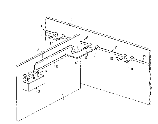
In the F gure, only one plug-in ~odule or component 1,
of the many plug-in component~ that are acc4mmodated next to
one another in a mag~zine ~not shown), i~ illustrated. Each
of the plug-in modules 1 is provided with a plurality of
electrical components 2 of which only one, e.g., an in-
tegrat~d circuit, i8 shown. The plug in modules 1, which as
shown basically comprise a printed circuit board with its
components, are further provided with multi-pole plug-in
connectors which extend along the edge of the resp~ctive
module or circuit board and which are generally configured as
vertically extending columns of contact or connector pin
strips. Only two contact elements, i.e. connector or contact
pins 3 and ~, of ~he connector of the illustrated plug-in
module 1 are shown. Also not ~hown are the insulated
component~ in which th~e connector pins, are embedded in a
conventional connector.
~3~3Zf~2
On or adjacent the rear wall of the magazine (not
~hown), there i~ provided a rear wall circuit board 5. This
aircuit board 5 ~ provided with mating connectors, i.e. in
the form of ~ocket connectors with socket contacts in the
illu~trated embodiment, to match the ~ulti-pole connector
for each respective plug-in module. Only two contact
ele~e~ts, i.e. contact sockets S and 7, 8 and 9, and 10 and
llt o~ each of three adjacent socket connectors on circuit
board 5 are ~hown. Additionally, not 6hown are the insulated
bodie~ in which these contact ~ockets 6-11 are embedded in a
conventional connector.
Rear wall circuit board 5, o~ which only a part i~
shown, i~ provided with bus bar sections ~n the ~or~ of
printed conductors. Bus bar sections 13 and 14 are ~hown in
their sntirety,~while bus bar sertions 12 and 15 are shown
only in part. Bus bar section 14 connects only the contact
element or ~ocket 9 of one ~ocket connector with the contact
element or socket 10 o~ the adjacent ~ocket connector for a
further plug-in modula 1. In a similar manner bus bar
section 13 connect6 only contact element 9 with the contact
element 7 of the other adjacent socket connector. Generally
~peaking, each bus bar ~ection connect~ together one contac~
element of each of two adjacent 60cket connector6. It is
under~tood that the rear wall circuit board 5 i~ provided
-- 6 --
,
/
~3~g3Zf~Z
with ~urther conductor~ ~not shown) which connect the non-
illustrated contact element6 of the respective socket
connectors with one anothex.
Connector pins 3 ~nd 4 of the illustrated plug-in module
1 are plugged into and engage contact socket6 8 and 9,
respectively. According to the invention, a first conductor
16 leads from contact pin 3 to a terminal pin 17 of the
int~grated circuit component 2, and a 6econd conductor 18
leads from thi~ terminal pin 17 to contact pin 4. The non-
illustrated plug-in modules whose pair~ of connector pins
corresponding to pinC 3 and 4 engage in sockets 6, 7 and 10,
11, respectively, and into further non-illustrated sockets
pair~ for the bus bar, are configured in the ~ame manner.
With the described arrangement, a complete bus bar is
created only if all plug-in modules 1 for a bus bar are
plugged into the circuit board 5. The bus bar is composed o~
bus bar sections (e.g., 12-15), aontact fiockets (e.g., 6-11),
contact pins (e.g., pins 3 and 4 and the corresponding pairs
of pins for the ~ocket pairs 6, 7 and 10, 11) and the ~irst
conductor 16 and the second conductor 17 on each respective
module 1. Due to the respective line pairs 16, 17, such a
bus bar has no stub lines whose length must be considered
with respect to the wavelength of a high~frequency signal to
be transmitted over the bus bar. Thus, there are al50 no
- 7 -
~3g;13~
27371-189
raflection points created by such stub lines and their
disadvantageous effects, ~uch as, for example, reflections.
Although terminal pin 17 snd its extension within the
integrated circuit 2 do form a stub line, its length is
negligibly short.
The present invention thus make~ it possible to arrange
electrical components at any desired locations on a plug-in
module and to supply them with a high-~requency signal via a
bus bar7
In the illustrated embodiment, only a single-pole bus
bar is described. However, it is to be understood that
multi-pole bus bars can be set up in the same manner.
Moreover, a plurality of such single or multiple pole bus
bars may be pro~ided in the same system.
The invention now being fully described, it will be
apparent to one of ordinary skill in the art that many
changes and modi~ication~ can be made thereto without
departing from the ~pirit or scope of the invention as set
fcrth herein.