Note: Descriptions are shown in the official language in which they were submitted.
~3~3~48
TITLh ~ TH~ 7~ ION
SEMICONDUCTOR HEAT DISSIPATLNt~ APpARATus
BA(~KGROU~ID. ~ TH~ N~ION
Fteld o~ the Inventi.o~.
The pre~ent inven.t.ion relates to a.memher for a
.semiconductor ap~aratus, and more particularly, it rela~es
to a mem~er for a semicon~uctor ap.~aratus such as a
circuit suDstrate~ which mus.t be of hl.gh therml
conductivity to be mounted with a semicon~llctor device o F
high calorific power such as.a high.-power transistor or-a
laser diode..
De~cr1ption of the Priox Art
A member or a semiconductor ap~aratus to be msunted
with a semiconductor ~e.vice is generall.y formed h~ an
insulating mem~er and a radiating membe~ joine~ to the
insulating member For exam~e~ such-a memhe~ ~or a
semiconductor apparatus is forme~ by.a~ ins-~lati.ng
substrate to be provided thereon w_th a semicon~uctor
device^and a radiating substrate joine~ to the ba¢k
surface of the insulatin~.su~str.ate b~ soldering th~.o-lgn
silver solder or the like. In this case, generally
reguired for the insulating s~bstrate are high electri.c
insulaDility for insulation Erom the semicon uctor device.,
high m~chanical.strength and high thermal Col~UCtiVity for
dissipating heat generate~ from the semico~duct~r de~tc~.
-t` ~
~i~
13'J33~B
~he radiating.subs~rate mu.st have high thexma.l.
conductivity similarly to the insulating su~s~ra~e, whLle
its.thermal expansipn.coef~icient must be approximate~to
those.of materials.form.ing.a.semiconduc.tor:substrate; the
insulating substrate and the like.
In general, alumina tA12O3) is selected as a material
satisying the af~rementioned properties ~or forming the
insulating subs~rate employed in such:a mer~ber for-a
semico~ducto:r appa~atus. However, although alumina.is
excellent in elec~ric insula~i.lity and. mechanlcal
strength, its heat dissi~ation pro~erty is inferior-due to
small thermal.conductivity of 17 Wm 1K 1. Thus, it is
improper to carry a field-e~fect trans~stor ~FET) o~hig~
calorific power, for exa~ple, on an alumina subs.~rate.. In
order to car.~ a semiconduc~or-device of hi~ calorific
; pow~, another type o~ ins.ulating substrate is preparecl by
bexyllialtBeO) having..high therma~l conduc.tivity of 260
Wm lK 1, whe~eas ber~llia.is toxic and hence it is
troublesome. to take.saf.et~ measure~ in emp.lo~m~n-t of.such
an insulating substrate.
The radiating substrate is generall.y pxepa3.e~ ~ a
material satisfying..the aforeme~tione~ propertie~ which
material is selected from metal.mat.erials-s~ch as various
types of copper:alloys, copper-tungsten a~lc~ys.and
copper-mol~bdenum alloys. For examyle, Japarlese~Paten~
-- 2 --
13~3Zf~
Laying-Open.Gaze~te No 21032/198~-discloses-a.-subst~a'ce
o high therma.]. conduc:tivity for.carrying~.a-.semicond.uc.tor
device-, the material of which is pre~ared by rnixing~2 ~o
30 percent by weight of copper into tungs.ten or
molybden~.. Th~s substrate is employed.as.a~.radiatiny
substrate which-is suita~ly joined to an al~ina-s~bs~rate
having inferior heat dissipation- property, and di~ere~
in thermal expansion.coefficient.be.twee~ the. 5 ame.and
alumina is relativel~-small. Thus, this prior:art exam~l~
is.insufficie~t in heat..dissipation property, which is
required.entirely over. a substr~te.For:car~yin.g..a
semiconductor- device.
In recent years, nolltoxic aluminum.ni.tride (AlNi) has
ge.nerated g~ea.t interest.as a ma~terial.for such an
.insulating sub~trate or carrying~a sem.~co~uctor device
of high.cal~rific.power because of its high the~mal
conductivity o:E about 200 Wm lK 1, which value is
substantial.ly e~ual. to that of be~ryllia, as well as its
electric.insulabi.lity and me.ehan~.cal streng~h:which are
e~uivalent to those of alumina.
Howeverj when an alumi~um nitride su~stra.e provide~
~with. a me.tallized.layer..is..soldered by a.solderin~.me~al
such as gold.solder or.silver solder, for-examp.le~ to a
generally.em~loyed radiating subs-~ra:te of a
copper-tungs~en.alloy or cop~er.--mol~bd.enum..allo.
13~33Z~3
containi~g 10 to 25 pexcent by weight~of cop,-~er, the
aluminum nitride substratc.may be~crack~d or.the rad,iating
substrate o the copper-tungsten alloy or the
copper-molybdenum alloy may be warped.
5 Such a p~enomeno~:resul.ts.. ~rom.therm~.stress.. cause~
-. by difference in thermal expansion coe~icient between the
copper~tungsten allc>y or the copp~r.~mo.lybdeIIum all.oy~and
aluminum nitrid~ during a cooling step upon soldeIing,,
which is performed at a temperature of 500 to 950C. This
thermal stress. may~co~cei.vably be.left.in th.e.alumin~m
nitride substrate as tensile residual stress; to crack the
aluminum nitride substrate and/or warp the radiating
substr~te of the copper-tungst~n alloy.or the
copper-molybdenum alloy.
When an aluminum nitride suhs.t~.ate is joined to a
radiating..substrate of a copper.-tungsten~alloy.or a
copper-m~lybdenw~ allo~ by cold.solder~n~ or~soldering,
the alumin~ nitride substrate~or an interace~between;the
same and a meta.lliæed:,layer.is cxacked..b~ a~the.rm~ c~cle
20 test (-55C.to +150C, lOOO cyc~es~ or.a the~mal.shoc~
test to cause a.significant.p~oblem.-in prae~.ice:; even if
no warp nor crack is recogni.zed upon joining.
In.a sam~le o~ an aluminum nitride~substrate joined
to a radiating..substrate of a ~opper~tungs~en~alloy or a
copper-molybdenm alloy by silver soldering, thermal
~3~3Z~
fat.igue or thexma.l stress was cause~ in a.thermolcyc~e
test or~a thermal shock test due~t~ difference~in thermal
expansion coef~ic.ient~between~the radiat~ng subs.trate of
the copper-tungstPn.alloy or.the coppe~ molybdenum. al.loy
and the aluminum nitride sub~.trate, similarly to the
above. Such a problem of. thermal. stress or thermal
fatigue.is aggravated with increase. in junc.tion:area.
Thermal.expansi.on~coefficients of the coppe~r-tungsten
alloy or the copper-molybdenum alloy hav.lng the
aforementioned composition and aluminum nitride.are 6 . 5 to
10 X 10 6tK~ and 4 to 5 x 10 6/K respectively, w.ithin. a
range of the room temperature to about ~50C. Further,
these materials, having high Young`s~modulus of 27000 to
35000 IC~mm2 ancl 35000 to 37000 Kg~l~n~^ res~ecti.vel~, ar.e
hardly~plastically de~ormed.. Thus,. when the
copper-tllngsten. all~y or the copper-molybdenum alloy of
the.aforementioned.compositio~ and aluminum nitride!are
joined with each other b~ soldering-j large therma~ stress
is conceivabl~ caused in.a cooling step.
SUMMAR~.OF THE.INVENTION
; An object of the~present inventio~-is to prQv de-a
member for.a semiconductox. apparatus by employ~ng an
insulatiNg member o~ aluminum.nitride having.excellent
heat dissipation property to be-mounted with a
semiconductor device of high cal.ori~ic power, so that a
31 3~:)3~
radiat.ing member main~ ~ormed of a rneLal. ma.terial. havil~y
hlgh hea-t. radiation property can be~joined to the
insula~ing member with no.crac~ nor-warp.
The~inventors have-made-deep stud~ to solve-the
aforemelltione~ problemj to find a metal materia~ ha.ving ~
therm~l..expansion.coef~icient sub~.tantiall~y.equal.to that
of aluminum ni.tride and high.heat radiation property,
which material is suitably applied to a.radiating~ memb.er
to be joined.to.an insulating member.:o~.aluminum.nitride
for preventing cracking or~warping caused by the~mal
stress in a cooling step upon-solde~ring~.
A member for.a.semiconduc.tor. appa~atus in acco~dar-ce
with the present inventiorl, being adapt:ed to car:ry~or hold
a semiconductor devlce, comprises an insulat.ing~mem~er o~
aluminum ni.tride..having.a major surf~ce..to ~ace~.the
semiconductor devic~ and a radiatirlg mem~er, to be~joined
to the insul.atin-J me~ber., mainly formed of a meta:l
material hav.ing thermal.con~uctivity of at l~ast 120 Wt~K
and a. thermal expansion.coefficient within;.a..range;of.4.to
6.0 x 10 6~K. The thermal. eY.pansion coe~ficient o~ the
metal material formin.g.the~radiating member:joined.to.the
insulating member is so selected to be within..the above
range that.the same is.. substantially~e~ual to that.of
. aluminu~ nitride, whereby the radiatin~ membe~is not
deEormed and no crack is caused in the~insul.ating mem~er
~ 6 --
.. ....... : ,. - ,
~L3~3Zf~3
o~ aluminum nitride in junction through sol~lering-. In
view of heat radiation property, t`nermal cond~uctivit~ of
aluminum nitride.joined to.the.radiating..member:is,within
a range of 120 to 280 Wm lK 1, and henc~ the entire memb_r
in accordance with the present.invention can be~ retained
in high heat radi~tion property.
Preferably the metal material forminy the radiating
member.includes, tungst~n. The. the~:ma.1. expa.nsi.oII
coeficient of.tungsten~is 4.~ x 10 61Kj which value is
substantially e~ual.to~that o~ aluminum.nitride.. Thus.,
even if an alumin~n nitride substrate.i.s joine~ to a
tungsten me.tal.plate by sold~ring.at.800 to 950C, the
tungsten metal plate is not deform~d!and~.no crackAis
' caused in~the aluminum nitride,~bstrate.
The me.tal material.. forming.the.radiatin~.. member.. ma~
include a tungst~n alloy, which contains at least nickel,
copperj iron or cobalt. ~he thexm~l e~.p~ns~.on coef~icie~t.
of such A tungsten alloy is increased.as theicontent of.
the above metal componentls) is increase~, to extremely
dif~ex ~rom.that of~ aluminum nitride. Thus, the content
of each metal comp.onent is limited to be not more. than 10
: percent by weight so that the therma~ expansion
: coeficient of the~tungsten alloy is substan.tially e~ual
to.that of aluminum.nitri.~e.. If the. totalicontent~of on.e
2S or more such metal components is less than O.Ol perce~t by
~3~3;~
weight, a proh~.em is caucecl in machinabi.lity o~ a t~ng~ten
alloy plate.
Further, consideration mus.t be made-on thermal
conductivityr which is one of properties requirea for.the
radiating membe~ mainl~ formed of the tunysten alloy. The
content of~each metal component is limi.ted~ to be not more
than lO percent by weight, so.tha.t therma~l..conducti.vity~o~
the tungsten alloy is;at least 120 W~m ~: In view of
thermal expansion.coe~ficient, machina~ili.ty and thermal
.conducti.vity, the~ content of. each.metal.com~o.r~ent. lS
preferably within a range of ~.01 to 10 percent by weight.
In paîticular, the most pre:Eerable tungsten alloy contains
1 to 7 pexcent by we.ight o~.nickel.; O.l to 4..percent.by
weight of copper and 0.1 to 2 percent by wei.ght of ironr
It ha~ been recognized tha.t the thermal exparls.i.on
coefficient is extremely.irlcreased.in a.tungs.ten alloy
obtained by adding at least 10 percent. by we~ight~o~ coppe~r
to tungsten.
The thermal expan~i.on.coefficient of a
. 20 copper-tungsten alloy containing only copper-is incre~sed
with increase in the content of copper. to extre~e~y
differ from that of.aluminum.nitride.. In.order to att.ain
a thermal.expansion co~ficient substantially~equal to
that of alumin~u~ nitride,-it is optimum to em~lo~ a
radiating member mainly formed of a copper.-tungsten.alloy
-- 8 --
13~3Z~I~
containing 0.1 to 5 percen~ by weiyht of~cop~er; I~ t~e
copper content i5 not mo~e than 0.1 percent by we!.ig~t,
- cutting work~of a copper-tungsten alloy pla.te~is dif~icult
while thermal conductivityj which is an excellent property
of the-copper--tungsten alloy plate, is reduced. If the
copper conten:t exceeds 5 percent-by weiyht, the thermal
expansion coe~ficient o~ the cop~er-tungsten-alloy excee~s
that of a~uminum nitride,.as.hereinabove descri~edO
The metal material.forming the radiatirlg member:ma~
include molybdenum. The thermal. expansion coefficient of
molybdenum is 5.5 x 10 6/K, which value is su~stantially
equal to that oE aluminum nitride. Thus, even if an
aluminum nitride substrate is.joined to a molybdenum me.tal
plate by soldexing at 800 to 950CI the molybdenum metal
plate is not deEoxmed and no crack .is caused in the
aluminum nitride substra.te.
The insulating member o aluminum ni.trid.e is
preferably employed:as a.substrate.havin~ a major. surace
to be provided thereo~ with a semiconduct~r de.~ice.
Alterna.tively, the insul.ating mem~er ma~ be applied to a
co~ering.member.provide~ ab~ve.a.semicondu~.~-or.de~ice to
protect the same., which covexin~ member ~orms a-cap for
airtightly seal.ing a.semiconductor device provi~ed on an
insulating.subs.trat~, for example.. When:the insulating
member is employed as a substrate for carr~ingia
~L3~3Z48
semiconductor de~ice or a covexing memher for.:prote~ing a
semiconductor devic~, the inventive me~er for a
sem:iconductor apparatus is-adapted to conduct heat
genexated from the semiconductor.dev.ice to the insul.atin~
member and a radiating member; thereby~to dissi~ate the
same~to the exterior. The insu~ating membel of alum.~n~n
nitride preferably includes a sintered bod~-.
The insulatin~ member of aluminum nitride is
preferably provided on its junction:surface wit~l a
metallized layer, which contains at least tungste~ or
molybden~, at least one aluminum compound:within aluminum
nitridej aluminum.oxide and alum.inum oxynitride, and
calcium ox1de or.yttrium oxide, to attain pre~era~le
~unction strength and~t~hermal..conductivity~
The inventive mem~er for a semi.concluctor appa~atus
further. comprises a solderlng..member.fo~.~o.ining.the,
me~allized layer.to the radiating m~l~erj and a plating
layer is provided~in a junction sur.face o the metallized
layer with a.soldering..member to.uni~ormly perform
stabili2ed-solder.ing. Namely, wettability between the
soldering member and the-metal.lized layer can be improved
by provision of the plating:layer.. Another plating:,lay,er
provided in a-junction surface~of-the radiating member
with the soldering.mem~er functi,ons;similar.ly to..the
above. Such plating.,layers.are preferably formed.by
-- 10 -- .
~3~f~
nickel plat~ng. Such nicXel plating is pr~fera~ly
performed particularly when processinglsuch.as.gold
plating is performed in a later. step, in order to imyrove
adhesion and precipi.ta.tion prop:e~.ties of gold plating for
forming a uniform go~d..plating..layer.
According to the-inventive member ~or a semiconductor
apparatus, a.metal material having prescri~ed thermal
conductivity and.thermal. expansion: coe~fici.ent- is.emplo~ed
as-a main material or forming a radiatin~.~mem~er.j ~hereby
to prevent cracking of the ins~lating.member. and warping
of the radiating member upo~ joining.of: the. insulating
member of aluminum nitride and~ the~radiatin~ mem~er.
Thus., a reliable memb:e~ Eor a sem.i.conductor: ap~aratus can
be easily.obtained..to.be app.lied to a.~subs;tra..te.for
carrying a semiconduc.tor device~, a coveriny men~e~r;for
sealing a semiconducto~ device or the like~
These.and other objects, features, aspe.cts..a~d
advantages o the present invention will become more
apparent from; the following detail.ed descri.ptiorl of the
. 20 present invention when taken in conjunc.~ion with. the
accompanying drawings.
BRIEF DESCRIPTION OF THE DRAWINGS
Figs. lA and lB are process drawings..schem~.tically
showing two exemplary methods of manufacturing a m~m~er
~3~`03~f~
for a scmlconduc~or apparatus.in a~cordance- w.ith the
present inven-ti.on;
Figs. 2Aj 2B and 2C are a plan view and sectional
views showing.an example~o juncti.on structure in a member
for a semiconductor apparatus in accordance~with t~e
present invention, such as junction:structure be~wee~- a
lead..~rame~, an aluminum nitride substrate ancl a radiating
substrate;
Fig; 3 .is a sectional view show~ng an~embodim~nt of a
member;for a.semiconductor. apparatus in accordan~e..with
the pxesent invention, which.is applied to a-hea.t sink
member ~or a semiconductor~ device such as a light emitting
diode (LED).or.a.laser. d.iode. (LD);
Fig. 4 is a s~ctional view s}lowing anoth~r embodimen~
of the inventi.ve member.~$or a sernicollductor appar.a.tus,
which is applied..to. a.paxt o~ a cap..fox..airtightly.sealing
a semiconductvr de.vice to serve as a covering memb.~r; and
Fig. 5 is a side elevational view showing a portion
subjected to measuremen~.of a warp caused in.a.radiating
member joined to an aluminum nitride substrate.
DESCRIPTION OF THE~PREFERR~D EMBODIMENTS
As:hereinabove describedj the present invention is
adapted to improve~the technique of formin~ a mem~er fo~ a
semiconductor apparatus by emp~loying an inslllatiny memh~r
of aluminum nitride. Alum~inw~ nitride.employed in the
- 12 -
. ~ . . . r . . ~
~3~3;~
form o a sintered body in the present invention is
obtained~by the following method, for example:
The;insulating mem~er formed by an.aluminum nitride
sintered body emplGyed in the~present invention,
preferably being.mainly composed o aluminum nitride,
contains 0.01 to 1.0 percent by weight of~an element
belonging to the group lIIa of the periodic table and
0.001 to 0.~ percent by weight of ox~gen, and its thermal
conductivity is at least 180 Wm lK 1 First, at least one
compound.containing a rare earth elemcnt is.mixed with
powder of aluminum nltride so that its con:tent is 0.01 to
l.O percent by weight~in rare ear~h element~conve~sion. A
form.ing addi.tive is prep~ared by paraphine, PVD o~ PEG
substance; such as phenol resinj being decomposed to leave
carbon, carbon powder, graphite powder: or the~like may be
added.to..control res.idual carbon:in the.sinte~e~ bod~.
The rare~earth~compound is prepared by stearic acid,
palmitic.acid, alkaxide nitrate, carbonate, hydroxide or
, the liXe. Pre~erabl~ employed is. a.high.molecul.e compound
such as stearic acid. Such.a compound is conceivably
adapted to reduce the content of the~rare:earth element to
enable.good mixing..with aluminum nitride-pow~r. In
particular, steari.c acid.is most preferable:in view o~
mixability with alumin~n nitride powder, the amc~unt of
residual carbon etc in addition:.to its func.tion.as a
- 13 -
~32~
forming additive. The aluminum nitride powde~ must beformed by fine uniform parti.cles. Preferably its average
particle size is not-more than 1 ~mj and the oxygen
contenk is not more than 2.0 percent by we~ight. Such
aluminum nitride powder. is obtained;by a reduc.tion
nitriding method (method by reduction nitriding.of
aluminum oxide), since it is difficul.t to obtain the same
by.a direct nitriding me.thod:(method;by.nitriding.o~..met:al
aluminum). In order to ob.~ain the po~der by the dire~t
nitriding method, sufficient considexati.on:mus.t~e made-on
reaction control, classification of the..par:ticle.size and
the like.
Then the rnixed pow~er is shaped into a prescribed
configuration and. sintered.in a non-oxidizing..atmosphere
containing nitrogen~ In order to attain high:thermal
conductivity, it is preferable to sinter the substance at
a temperature o:E 1000 to 2100C for at least five~hours-r
so that its average particle size is a.t least 5 ~m. Af~el-
such sinteriny., it is~preferabl~.to quickl.y c~rry out.a
20 cooling step. If the su~stance is slowly cooled, a
sintering additive is precipitated and the sintered face
is extremely.deteriorated. Therefore, the sintered.bod~
is pxefera~ly cooled to a temperature of 1500C at-~ ra~e
of at-least 200C/h.
- 14 -
~3~3;~
The steps of form.ing a met.a~lized layel- on the
surface of a su~strate formed by the alumi.num nitride
sintered body o~tained in the.a~oremention~ed manner are
performed.as foll~ws:
First, a subs*rate of the-alumin~ nitride-sinte~ed
body is~prepared by the aforementione~ method. A ma~erial
Eor the metallized.layer. is.pr.epar.ed..by kneading.powdcr.o~
a calcium compound, that o~ an aluminum comp.oulId:and metal
powder of.tungs.ten or.molybdenum with addition of an.
organic binder such. as vehicle,.to provide metal.paste.
The contents of the respective~components-may be~within
the ranges of 40 to 98 percent by weight oE the me~al
powder:, 1 to 25 percent by weight of the aluminum.compound
and 1 to 35 percent by weiyh:t o~ calcium oxide. In order
to per~orm a late~ s.intering ste~ at a~low~-tem~erature,
coppe~.or nickel ma~be~ added~as. a catalyst~or reducing
the sintering tempera~ure. The metal paste thus~prov'ded
is applied to the sur.face o~ the substrate ~ormed by the
aluminum ni.tride sinter.ed body. The.substrate;formed by
the aluminum nitride sinte~ed body-is fired in an inert
atmosphe.re o~ nitrogen- or the like at a tempe~ature o~
1500 to 1800C, to be provided with a meitallizea layer.on
its sur~ace. A metallized layer prepared by me~al pow~r
. - o~ tungs.ten and containing 1 to 10 p~rce~t by weight o
aluminum oxide, employed as th.e aluminum compound, and 1
- .
~3~
to ~.0 percent by weight of calcium oxide, or that pre~red
by metal powder of~molybdenum and containing-1 to 10
percent by weight of aluminum oxide, emplGye~ as-the
aluminum.compound, and 1 to 35 percent by weight o~
calcium o~ide is preferable in view of adhesion between
the substrate formed by the aluminum nitride sintered body
and the metallized layer and thermal. conductivity.
The steps o forming a metallized layer on the
surface of a substrate formed by the aluminum nitride
sintered.bod~ may be performed.as.fol~ows:, by;sin.tering..an
aluminum nitride formed~body coated~with the metal paste
at one time.
~irst, a substrat~. o~the. alumi~um nitride-formed
body is pr~pared by shaping theiaf.orementione~ mixed
lS powder into a prescxibed con~iguration SUC~ as! a green
sheet. A matexial ~or the metallize.d.layer.is;.prepa~ed:by
kneading powder of tungste~and at least one add~iti~e
selected ~rom a group o:~ al~nin~m oxide; aluminu~ nitri~e-,
calcium oxide, yttrium oxide and stearic.aGid.yttr.ium and
the like, to provide metal paste, similarly to the above~O
The metal paste thus provided is-applied~ to-the surface-o~
the substrate formed~by the aluminum ni.tride.formed:.body,
by printing or coating. The substrate formed by the
aluminum nitride.formed body is sintered with-the-metal
paste similarly to the above conditions, to be provided
~ 16 -
~3V3;2 ~
with a metallize~ layer on the surface of a substrate
formed.by the.aluminum.nitride sintered.body, Thus, the
aluminwn nitride sintered body with the metallized having
high thermal conductivity can be obtained.
Description is now made.on a typical method. o~
forming the:member for a semiconductor apparatus in
accordance.with the present invention. Figs. lA and lB
are process.drawings..showing..two methods. of:manu~.acturing
the member for a semiconductor-apparatus-in. accordance
with the present-invention. Referring to Fig. lA, an
aluminum nitride,sin.tered substrate.is fir.st pr.epa~red.
Then, the metal paste obtained through-the;-aforementioned
method is applied to the surface.of the~ alumim ~ nitride
slntered.substrate. Therea~ter..the,.me~a~ pas.te,thus
applied is dried, Then the alumin.um nitride sintered
substrate.is ~ired in an iner.t gas. atm0sph~.e which is
heated.to a prescxibed.temperature.
Theiabove steps may be performed as follows.
Referring.to Fig..lB., an aluminum nitride formed substxa~e
is ~irst prepared. Then, the metal paste obtained throu~
the aforementioned me~hod is applied~ to the~ surface~ o~ the
aluminum nitride formed substrate. Therea~.ter the metal
. paste.thus.applied.is.dried... Then the-aluminum nitride
formed substrate is sintered with the~metal. paste in an
25 inert gas.a.tmosphere which is heate~ to a prescribed
- 17 -
3L3~!i3;~
temperature. Thus, an aluminum nitride sinter.ed substrate
w.ith a metallized layer is foxmed.
After a metalli~ed layer:is formed on the alumlnum
nitride sintered substrate, nickel plating is performed on
the surface-of the metallized layer; Heat treatment-is
performed at a temperature of about 800C to sinter~the
nickel platin~, thereby tolimpl-ove strength and
airtightness of the~same. On: the other. hand, nicke.
plating is also~performed on:-the~surface of~a hea.t sink
member, serving as a radiating.member:, which is joined to
the aluminum nitrid.e.sintered substrate, sim~larly to the
above. Then~soldering is performed on the nickel plating
surface in order to join the aluminum nitride sintered.
substrate to the.heat sin~ mem~Qx. Fuxther, gold plating
is performed on such junction. Thus, the member~for a
semiconductor appara:tus in accordance!with the presen.t
invention can be manuactured.
Description is now made on an embodiment of a member
for a semiconductor apparatus in a.ccordance with. an aspect
of the present inventionj which is manufactured along.t~le
aforementioned~stepsi, such as a memb.er compr1sing an
aluminum nitride~substrate joined to a lead fxame-on its
: surface and to a.heat sink member on. its.back.surface.,
with reEerence to the drawing~:.
- 18 -
~3~)3~
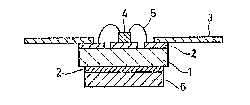
Fig. 2~ is a plan view~showing..an en~odi.ment whi.ch is
applied to a substrate for carrying a semiconductor
dev.ice, Fig. 2B.is a sectional view~of the substrate-and
Fig. 2C is a sectional view~showing..a~junction between,~
heat sink member 6 and an aluminu~ nitride substrate 1 in
' detail. Re~erring to these ~igures., the aluminum-nitride
substrate 1, impleme~ting.the inventive membeir: for:a
semiconductor apparatus, is partial.ly formed on- its
surface~with a metal.l.ized layer 2 in accordance with the
aforementioned.stepsj and a lead frame. 3 is.joined.to the
metallized layer 2 through soldering by a.soldering metal
or the like. Another metal.lized layex 2 is forme~ on a
part.oE the.bacX.surface,o~ the, aluminum nitride.subs;trate
1 in acco.rdance with the a~orementione.d.steps, while the
heat sink member 6 .~s joined to the metallized layer 2
through solder.ing.by a solderin~:metal or.the~like~. A
semiconductor device 4 such. as an FET of hi.gh;calori~ic
powex is carried on a prescrlb.ed posi.ti.on of th~ al.umin~
nitride..substrate 1, to be connected w.ith. the..me,talliz~d
la~er 2 or the lead rame~3 by a bonding wire~5. As sho~r
in.Fig. 2C, a thin plating.layer 8 is foxmecl on the
. metallized.layer 2 in the.junction between.the alumimlm
' nitride substrate 1 and.the heat si.nk-member 6, while a
platin~ layer 7 is formed at need on the sur~ace- o~ the
- 19 -
~3 t332~1~
heat sink member o, in order to stabilize wettability of a
soldering metal 9.
Descrlption.is now~.made.on another embodim~nt o~ a
mernber for a ,semiconductor appara-tus in accordance-with
another aspect o.~ the present:invention, whi.ch is appli.ed
to.a radiating..substrate.for car.rying...a semiconductor
device~such as a;diode having~high calorific power., for
e~arnple, with re~er.ence to Fig. 3. Referring. to~Fig. 3,
an.aluminwn nitride.substrate l.is.mounted.on,a heat~sink
memberl6, serving as a radia.ting:member mainl~ forme~ of
the metal material.in accordance with the~present
inven.tion,.through a me~tallized; ~ayer..2..similarly to.,the
abovej while a sem~condu.ctor de.vice 4 such as a 1ig~t
emitting diode (LED) or a laser.:diode~(LD) is~joined on
the aluminum.nitride subs~rate.1. The semicond.tlc.tor
device 4 is joined on another me~alllzed la~er 2 which is
~ormed on the surface of.the alu~inum nitride~subs~trate 1.
In this.case.j the.al~ninum..nitride.subs~rate.1 serves.as a
heat sink member. The~aluminwn nitride~substra~e 1 and
the heat sink member 6 are joi.ned with each other in a
similar manner...to.the.above.desc.ription with refere~ce:.to
, the junctîon structure between the al.uminw~ nitride
substrate provided.with the lead frame and the heat .sink
mem-~er..
- 20 -
13~3;~
Descr.iption is~now made on the structure oE a cap~to
which a member for a.semiconductor.apparatus.in accordance
. with the-present invention is applied, with reference-to
: Fig. 4. A metal.lized layer 2.is prov:ided on the surface
o a peripheral. edgeiportion of a covering..membe~
~ormed by an aluminum sinter.e~ body. A frame mem~er:13
formed by a layer of a metal.such as an iron~nicke~ alloy
i5 joined to the.metallized.layer 2 by a soldering.metal
or the like. The lower end of the frame member~13 is
joined to a ceramic substrate 101 through-another
metallized layer. 2~ A semiconductor device:4 is carried
on the ceramic substrate 101. A heat sink mem~er-6 is
mounted on the upper suxface of the covering member 11, so
that heat generated.~rom the semicondu¢.tor~de~ice.4~is
dissipated by the~heat~sink mem~er~6 through~the~ coverin~
member. 11, to.improve~a cooling effect. The covering
membe~ ll.oE the.aluminum.nitride~sintered.body.an~..the
heat sink member 6~are joined with each other in a similar
manr~er to the above des.cription with reference to the
junction.structure.between the-al.uminum.ni.tride substrate
. provided with the lead ~rame and the hea.t sink mem~erO
The soldering metal employed for such~junction is
preferably prepared by silver. solder, while another
. soldering material-is also avai.lablR so far as a thi.n
metal coating layer-having good wettabi.lity to the
: l3~1)32~
soldering material.can be formed on the junction sur~ace
oE the heat sink memher 6 o.r the metall.ized layer 2 to
strongly join..the covering memb:er 11 and. the.hea.t sink
member 6 with each other.. The function~of such a thin
metal coating layer, such as a plating layer, is as
hereinabove described.with.reference.to the example.of
junction structure bet.ween the aluminum nitride substrate
provided with.the lead frame~and the heat sink membe~.-.
Description.is now.made on Examples~..1 to 12j which
were carried out by employing samp~les prepare~ by
substrates o the aluminum nitride sinter.ed body ob.tained
by the aEorementioned.me.thod.
Example 1
~luminum nitride sintered substrates of 103 ~n-in
lS thickness were prepare~ by the. afor.emen-tioned me.tho.d~ to
be subjected to me~alliza:ti.o~l. The~metal.liza.ti.on.
processing was performed by applying metal.paste~of
prescribed.composition.to.the. suraces.of;respecti.~e
sarnples o~ the~aluminum nitride. sintered.s~bskra.tes,
per~orming debindering. and then~firing the same in a
nitrogen atmosphere at a temperature of 1600C for-60
minutes. Thus, metalli~ed layers were forme~ on
prescribed portions.of the~aluminum ni.tride-sintere.
substrates. - ~he metal. paste was prep~re~ by adding
calcium oxide~powde1-.and alu~ina.powder.to tungsten powder
- 22 -
~3q~3~
and kneading the same wit~l an organic binder.such-as
vehicle. The content o calcium oxide was 14 percent by
weight and.tha-t of alumina was 4 percent.by.weightO The
shapes of the employed aluminum nitride-sintered
substrates were 5 mm square, 20 mm sguare and 50 mm square
respectively.
Further, nickel plating layers of 2.~m in. thickness
were formed on the surfaces of the metallized la~er^s. On
the.other.hand, tungsten metal plate~s and.copper~tu~gst~n
alloy plates o~ 1.5 mm in thickness~wexe-prepared! as
radiating memb.ers to be jo.ined to the respective al]lm~num
nitride sintexed substrates. Nickel plating.of..2~m in
thickness wa~ performed on the~ s~lr~aces of the~Q me~al
platesj which.were then soldered to the~respec~ti.ve
aluminum nitride..sintered subs.trate~s by silver solder.at a
temperature~o~ ~30 to 9~0C.
Exam~nation..was made as to whether or not the
aluminum nitride. sintere~ subs.trates were cra~ked and
whe-the~ or not the tungsten metal plates~-and the
copper-tungsten alloy plates were.warped.in the.xesrpe~.tive
samples thus obtai.ned. As shown in Fig. 5j an aluminum
nitride sintered substra.te 1 and a heat sink member 6 of
each sample.were ~oined.wi.th each other.,.to.evaluate.the
deg~ee of warping..as the am~unt;a by a-surface roughness
tester (product-of Tokyo seimitsu: E-SP-S~lA). Cxacks
- 23 -
~3~3;~
caused in the respective aluminum nitrideisintered
substrates were observe~ by a scanning type eleetron
microscope~o~ 5000 magnifications.or a steromicx.osco~.e of
40 magnifications. Table l shows-the results. As to
S evaluation of wa~ps, those of-not more~than 2 ~m with
respec.t to.effective length of.l mm were xega~ded aC."no
warp", while sam~les causing warps exceeding 2. ~m with
respect to e~fective length o~:l mm were rega~ded as
"warped?'.
"lOCu W1' and "20Cu-W" in Table l repr~s~t reference
example.s, which were prepare~ by copper.-tungs.ten all.oys
containing lO.percent by weight an~.20.percent by weight
of copper respectively. The therma~.expansi.on coef.ficie~t
of the tungsten metal plates was 4~ x 10 6/~ and the
thermal conductivity thereof was 168 WlmK. The thermail
expansion coef~icients o~ the copper.-tungstenla.ll.oys
lOCu-W and 20Cu-W were 6.5 to 7.5 x 10 6/K and 8.5 tol9.5
x 10 6/K in the range of the room-tempera.ture to 950C,
xespectively. The.values o~ thermal.con.duc~ivit~.of-the
copper-tungsten alloys lOCu-W and 20Cu-W wexe-210 W/m~-and
246 W~mK respect-ively.
According to Table l~ the reerence.examp1.es prepar~ed
by joining the copper-tungste~ alloy plates respecti~ely
containing.10 percen.t by welght and 20.percent.by weight
of copper to aluminum nitride sintered substrates were
- 24 -
~3~3Zf~i3
warped and..crack~d.. On thc other hand, no.crack no.r warp
was caused~-in the samples in accordance with the prese~t
inv~nt.ion, which were pre~ared by joining.tung~ten metal
plates..to th~ aluminum.nitride sin.tered.substrate..
Table l
: Sample ShaEe W lOCu-W _ 20Cu~W~
O 5 mm no warp warped warped
(no crack) Ino crack)(crack~
. l
20 mm do. warped do.
(cracked.)
_
50 mm do. do. do.
Example 2
Gold.plating Oe 3.~ in.thicXness.was performed on
the surfaces of samples!prepared in similar shapes. to
Exampl~ 1. The metallization processing of samples!was
performed.by applying..tungs.ten.paste.o~.prescribed
composition to the sur~aces of respective samples of the
aluminum formed.-substra.tes.shaped in a configura.~ion such
as.a green.sheet by the.aorementioned me.thod with screen
printing of prescribed patterns, drying, performir.g
debindering and then sintering the same in a.nitrogen
atmosphere at a temperature of 1850C for 5 hoursO Thus,
- 2~ -
.. ., ... .. , . ~........... .. .
3 3~3Z~
metallized:layers were formed..on prescribed portio~s^of
aluminum nitride sintered~ subs.trates, Be~ore the~ abo~e
gold plating, nicXel plating layers of 2 ~m in.thic~ness
were ~ormed on the metal.lized.layers, and.si~tered,.in a
hydrogen atmosphere at a te~perature-of 750C for 2~
minutes.. Then:aluminum.nitride.sintere~.substrates were
soldered to tungsten metal. plates or copper-tungsten alloy
plates..by gold.solder.at a temperature of 450.to 550C.
Examination was. made as to cracks of the~aluminum
nitride sintered substrates and, warps~oE the tungsten
metal plates and.the the.copper-tungs.ten-.al.lo~ plates
similarly to Example 1. Tab].e 2 shows the~resul.ts.
According to Table 2, no warp nor.crack was~ caused in
the samples.ob.tained by,joining..the.tungs~te~ me.tal plates
to the aluminum nitride sintere~ substra.tes~in accorddn~e
with the p~esent invention.
Ta~le. 2
S le Sha e W lOCu-W. 20Cu-W-
np P ~ _ _ __
: a 5 mmno warp warped warped
: (no crack) (no crack~ (no crack)
0 20 mm do. do. warped
tcracXed~
. ~ 50 mm do do. do.
- 26 -
~13~3~,f~
A thexmo cycle test. ( 55C to -tl~0C, 100n cy~les)
was performed on the samples causing no warp nor~crack in
Examples 1 and ~, while no problem was.recognized~
Example 3
On samples subiected to gold plating similarly to
Example-2j soldering was performe~.by lead-indium solder
at a temperature of 250 to 300C, and therea~ter a thermo
cycle test (-5~C to ~150C, 1~00 cycles~ was.pexformed.
Structures in the interiors of aluminum nitride:sintered
substrates and metallized layer interfaces were obsexve~l
in the respective samples to evaluate~.the.degr.ees.of
crackiny and the states~of warps in tun~sten metal plates
and copper-tungsten alloy pla.tesi Table 3 shows~the
results. The method.s Oe. evaluatiny cracks.and.war~s.a~e
as described with .re~erence to Example l.
Accord.ing to Table 3, no wa~p nor craGk was
recognized in the.samples whi.ch were prepar.ed.b~.joini.ng
the tungsten metal plates to the~al~inum nitride sintered
substrates in acco.rdance with the present inven~ionO
,
- 27 -
... .~... . . . . .... ;. , .
:~3~32~3
Table 3
Sam le Sha e W~ lOCu-W~ 20cu-w~
P P
5 mm no.warp no warp . no warp
. Ino crack-)(cracke~ (cracXed)
20 mm do. do. do.
p 50 mm do. warped warped
. ~cracked-) (cracked)
Example 4
.Samples obtained.by.perform.ing...nickel.pla.ti~.g....of 2 llm
in thickness on aluminum nitrid~ sintered subs:t~ates o
1.3 mm in thickrless.prov~ided~ with me~alliæed layers
similaxl~ to.Example 1 we~re. soldered.to.tungs.te~ allo~
plates o 1.5 ~n in thickness having compos~tions as shown
in Table~4, the suraces.o.E which were~nickel~plated, by
silver solder at a temperature of 830 to 950C~
Examination was performed on the~respective.samp.les-.thus
obtained, as to.cracks!of the.aluminum.nitride.sintered
substxates and warps o the tun~sten allo~ plat-es. Ta~le
4 shows the results In the column-of.~th~ tungsten-allQy
plates.as shown in Tabl.e 4, or exam~le, `'~N~-lCu~W!'
xepresents a-tungsten~alloy containing 5 percent~by weiyht
of nickel and 1 percent by w~ight o~ copper~ Such
indication o~.tungste~.all.oy plates.also.appli.es.to Tables
- 28 -
:13~ Z~i~
5 and 6 concerning Examples 5 and 6 as here.ina~ter
describ.edO Symbol * indicates reference examples~ ~able
4 also shows the values of thermal. conductivity-~and
thermal expansion coeffici.ents of the tungsten all.oy
plates.
According to Table 4, no warp nor crack was
recognized.in the samples~which~were ob.tai~ed by joining
the tungs.ten..alloy plates to.the.aluminum..ni.tride
substrates in accordance-with the present~invention.
:
- 29 -
3~
Table 4
Thermal Thermal \ Sample shape C]5 mm U 20 mm ~50 mm
Condue~ Expansion Type \
tivit~ Co- I o~ \
(W/mK) effic~n~ w-Alloy
(xlO K ) Plate
5.5 5Ni-lCu-W* no warp no warp no warp
tno crack) ~no crack) (no eraek)
.
5.4 5Ni-lFe-W* do. do. do.
_
89 5.2 lNi-lFe-W* do. do. do.
. _
84 6.4 12Ni-12Fe-W* warped warped warped
~craeked) (erackad) (eracked)
120 5.2 2Ni-lCo-Wno warp no warp no warp
(no erack) (no erack) (no craek)
98 5.7 7Ni-3Cu-lFe-W* do. do. do.
_
151 S.l 2Ni-lCu-0.5Fe-W do. do. do.
~ __ _
108 8.4 lONi-12C~l-SFe-W* warped warped warped
(cracked) (craeked) (cracked)
_ _ _~_
142 5.0 1.8Ni-0.8Cu-0.9F'e-W no warp no warp no warp
~no crack) (no crack) (no crack)
_ __~
131 $.4 3.0Ni-1.6C~t-0.4Fe-W do. do. do.
_ _
96 5.6 7.1Ni-2.5Cu-0.4Fe-W* do. do. do.
_ _
- 30 -
13~32fJ~P~
Example 5
Gold pla-tin~ was perormed on the s~rLaces~of samp~.2s
simi.lar to those employed in Example 4, and then alum~num
nit.ri.de sintered su~strates were soldered to various,types
of tungsten alloy plates by gold solder at a temperature
of 450.to 550C. Examination was.made on the.resp~tive
- samples thus obtained, as to cracks-of the alumirlum
. nitride sinte~ed subs.trates and warps of the~vt'ungsten
: alloy plates. Table.S show~the results.
According to Table~5, no warp nor cra~ktwas
recognized in the~samples obtained by joining!the turlgsten
alloy plates,.to.the alum.imLm n:Ltride sintered~su~st:ra~es
in accordance with~the presen.t~invention.
A thermo cyale.tes.t.(-55C to ~150C, lOOO.cycle~.)
was made on the~samplesica.usirLg no.warp nor~crack in
Examples 4 and.5, whlle no problem~was recognized.
; - 31 -
~3V3Zf~
Table 5
~ _ . .
Ther~,al The~nal \ Sample s}lape ~ 5 ~n ~ 20 r~n C~50 n~
Conduc- Expan~ion Typ~ \
tivity Co- o~ \ .
~W~mK) efFic~en~ w-Alloy \
. ~xlO K ) Plate
5.5 5Ni-lu-W* no warp no wa~p no- W~L~P
(no crack) ~no crack) ~cr~ck~
: . 90 5.4 5Ni-lFe-W* do. do. do.
_ _
89 5.2 lNi-lFe-W* do. do. do.
84 6.~ 12Ni-12Fe-W* warpe3. wa~pe~. wa~p~d
. (no crack) ( no c:rack? ~cracked)
~ _
120 5.2 2Ni-lCo-W no warp no warp no warp
~no crack) (no crack). (no crack)
___ . _ I
98 5.7 7Ni-3Cu-lFe-W* do. do. do.
151 5.1 2Ni-lCu-0.5Fe-W do. do. do.
_ __ _ _
108 a.4 lONi-12Cu-SF~-W* warped.. warpe~ warped
(no crack) Ino crack) (crack~d)
_ _ __
142 5.01.3N:I-O:~Cu-0.9Fe-W~no warp no w~r.p no wa:cp
(no c.r~ck~ (no crac.k) (no.cr~e~k)
~ _ _ _
131 5.~ 3.ONi-1.6Cu-0.4Fe-W do. do. do.
~ .
96 5.6 7.1Ni-2.5C~I-O.~Fe-W* do. do. do.
_
- ~2 -
.
~3el3~
ExamPle 6
In the samples~whose~surface~ were s~l~jected~ to ~old
plating-in!Example~.5, aluminum~n~tride-s,intcred-subs,tra~es
were soldere~-with various-types~of tung~terr allo~ plates
5 by lead-indium solde~ at a temperatur~ of~250 to.. 300C, to
pe~^form.a thermo cycle~test t-~5C to +150C, 1000
cycles). Struc~ures in the.interiors.o~ithei-aluminum
nitride sintere~ substrates-and me~all.i2ed laye:r
interfaces were observe~ in the~ respecti~e-s~mple~r to
1o evaluate pxesence~absen~e of:cracks in the~al.uminum
nitride sintere~ substra.tes:and: the:states:.o~ warps;caused
in the tungs~en alloy plates. Table 6 show~q~the res~1.ts.
According.to Table 6, no warp nor cra.ckiwas
recogni.æed in the sampl.es o~t~ained~by joinin~the~tun~s~er
alloy plates~to the aluminum.n~tri.de,sin.ter0d substrate.s
in accorda~ce.:.wàth the~present;in~entio~.
:
- 33 -
~3~3;~
T~lble 6
Thermal Thermal. \ Salnple shape. ~ 5 l~n Q 20 m~. O SO mlm
Conduc- Expansion Type \
tivi ty Co- oE
(W/mK) e~fic~en~ w-~lloy \
(xlo K ) Pla~e \ _ _
9S 5 . 5 SNi- lCu-'W* no wa:~p. no w~rp S no w~rp
(no er~ck) ( no erack) ( no erack)
5.4 5N.i-lFe-W* do. do. do.
89 5.2 lNi - lFe -W* do. do. do~
84 6.4 12Ni-12Fe-~* no wa~-p no waLp warped
. .. ( cra~ kecl) ( cracke~) ( CrE~Ck~?t-})
120 5.2 2Ni-lCo-'.~ no war.p. no warp, no w~rp
~ no Cl'aC~C ) ( no craOEk) (no crae~)
_ . I _ _ ~ _
98 5.7 7Nl-3Cu-l:Fe-'~ do. do. do.
_____ _ I
151 S.1 2Ni-lCu-O.SFe~ do. do. ¦ do.
108 8.4 lONi-12Cu-51Fe-W~ no W~'Lp no warp war~ed
(eraehed3 (craeked) (erclck~a)
~__ ___ _ . __
1~2 5 .o l~Ni-a.8cu-o.9F~-w rlo.warp. no wa.rp. no warp
_ (no erack) (rlo eraek~ (no crack)
131 $.4 3.ONi 1.6Cu-0.4Fe-W~ do. do. do.
l - _
S.6 7.1Ni-2.. $Cu-O.~Fe-~'* do. do, d~.
- 34 ~
13V3%~1~
Example 7
Samples.obtained by per~ormlng. nickel platingi.of 2 ~m
in thickness on a~um.inum-nitride sintered substra~es-of
1.3 mm in thickness, which we~e;formed-with metalli.zed
layers.similarly.to Example.l,.were soldered.to
copper-tungsten alloy plates of 1.5 mm in thi.c~ne:ss; the
surfaces of-which were suhjected to n~cke-l plating of-2 ~m
in thickness, by silver.solder.~t a tem~erature.of 830 to
950C. Examination was~made~on the~respe¢ti~e samp~es
thus ob.tained., as.to c~ac~.o~.theialuminum ni.tride
sintered substrates and warps~of the-coppe!r-tungsten alloy
plates~by the measuring methods.as describe~ with
re~erence to Example.1.
Table 7 shows the!results. The types of the tu~gsten
~5 alloy plates and.evaluation of warps are indica.te~ in. a
similar manner to Table 1. "6Cu-W!', "lOCu-W" and "20Cu-W~`
represent~reference examples.
According to Table.7, no wa.rp nor crack~was
recognized.in.the.s~mpl2~..0b.tained-by joiningi.the
~o copper.-tungsten alloy plates to the alum num~nitride
sintered suhstrates in accordanc.e with the present
invention.
Furt.her, metallized layers of the aforemen.tioned
compositions were formed on;prescri~e~.surfaces~of:the
samples of the aluminum nitride.sintered subs.trates.,. and
~32~
nicXel plating layers of 2 to 3 ~m in thickness and.gold
plating.layers of 2.to.3 ~m..in thickness.w~re sequentially
formed on the-same. Thereater~ield.-e~ect high-power
transistors were solder.ed/carried- on-the s~rfa~es-~of the
S plating..layers.by go:ld-silicon:.so.lde~ing:.ma.terials.. In
.each sam~le, change.~VBE in forward e~fect v~ltage VBE
across:the~emitter.and the. base.~oE the transis.tor:caus~d
by power application was mea~ured by ~VBE me~hod, to
evalua.te thermal.resistance.of:the. entire prod.uc.t
integrally forme~ by the transi~tor; the alu~inum nitride
sintered subs.trateiand the copper:-tungs.ten alloy plateO
The..thermal resista~ce,vallle thus..measuLed in each sample
was not more than about 1.9C/W. Thus., it is understood
tha~ a.subs.trate;for..car.rying..a.semicond~c.~r:de~ice~is
suitably prepared~by an aluminum ni.tride s~bstra.~e, with
employment of.a co~p~r-tun~s;ten alloy.pl.ate as a radiating
subs:trate.thereEor, in view of..thermal.cond.uc.tivity.
. ~-- ~
- 36 -
~3~;~2`~
Tc~ r~ 7
_ ~ -
Th~3~m~l Thenna:l \S~nlpls ~hap~3 a s mm, . U 20 .rnn. . P S~ r
Conduc - Expansiorl Type\
tivity Co- of
(W/mK) e:EEi.c~ n~. w-~lloy \ .
(xlO K ) Plal:e
.
170 4.$ O.lCu-W 11~ warp. no w~rp, no warp
(no craek) 'no craek) (no erack)
172 4 d lCu-W ~ do. ¦ do. d-3.
_ _
174 S.l 2CIl-W do. . do. do.
_
180 6. 5 5Cu-W do. do. do.
_ _ _~
185 6: 6 6CIt-W no w~rp w*.rpe3 w~,t-~d
(no cr~ck~ (n~ cra-~l;) (cr~,k~d)
. _
210 7.0 lOC~-W w~.rped warp~d warped
. (no erack) (era-~k~.d3 ~erack~
_
246 9.~ 20CI~ W w~r~ed. do~ d~.
. _ (craeked)
Example 8
Gold.plating;o~ 3.~n.,in thick~ess,..was~...per~orme~...on
the surfaces o:E respective~sampl.es similar to th~se of
Exampl.e~7, and alumin.um nitride sintex.e~ suhstxa~es and
copper-tungsten alloy plates~.were.joined wi.th.each..other
by gold solder at a temperature o~ 45~ to 550C.
Examination was made.on:the respective~sam~le~..thus
obtained as to cracks of the aluminum nitrid~ sinte~ed
substrates and warps.o~ the copper-tungs~en alloy~pla.tesO
Table 8.shows.the results.
- 37 -
3L3~332~3
Accordlng to Table 8, no warp.nor crack.was
recognizediin t~e-samples obtained..by joining..the
copper-tungsten alloy plates to the.~alumin~ nitride
sin~ered substrates.in accorda-nce with the-present
inventi.on.
A-.thermo cycle test (-S5C to ~lSOC, lOOO cycles)
was performed.on.the nondefective samples o~ Examp~.es~7
and 8 causing no warp nor crack, while ~o prob~lem was
recognized-.
-
- 3a -
32~
'[~c,ble ~
_
Ther~n~l Th~rmal \ Samp?..e sh~e ~ 5 ~u~ 0 20 mm P 50 mn
Collduc- Expansion. Typ~ \
tivi~y C~- of \
(W/mK) efEic~en~ w-~lloy
(x10 K ~ Plat.e \ _
170 ~.S 0.1~u-W no w~rp~ no ~alp n~ ~ E'
~no erack) (~o ~raek) (no ~r~ck)
172 ~.8 1Cu-W do. do. do.
.
174 5.1 2Cu-W do. do. do.
180 6.S ~,u-W do. do. do.
1~5 6.6 6Cu-W do. do. do.
210 7.0 10Cu-W no warp no warpw~r~ed
~ ._ (no.e?rack) ~no cr~ek~ (no eracX)
2~6 9.0 20~u-Wwarped warp~d warp~d
(no ~r~.~ck) ~eraeke~3 (erack~)
Examp.le.9
.
Soldexin~ was!perEoxme~ on~respective sam~les
subjected to gold plat~.ng similarly to E~am~le 8 by
lead-indium solder at a temperature of 250 to 300C, to
thereafter perform~a.thermo.cy~e~test.(-55C.to.~150C,
lOOO cycles). Structures in th.e~interiors of the~al.uminum
nitride sint.ered substrates and metal.lized-layer
interfaces.wer.e.exami.ned in the respec.tive sampl.es..thus
obtained~, to evaluate cracks o the aluminw~ sintered
1o substrates?and waxps-of the~copper~tung~te~ allo~ platesO
Table~9 shows:.the.results.
. - 39 -
'~~
.
~3~3~
According to Tabl2 9, no warp nor crac.k.^was
recogni.zed:in.the samples~oh~ained.by joining.the
copper-tungsten allo~ plates to~the~aluminum-ni.tride
sintered.substrates in ac~cordarlce~lwi~h th~ present
invention.
T~hl~ 9
Thermal I'hermal \ Samp:le shape D 5 mm ~120 mm a 50
Condue- Expansion Type \
tivity Co- of \
(W/mK3 effie~en~. w-Alloy
(~10 K ) Plate \
170 4.5 O.lCu-W nc ~arp no ~ p . n~-wa~
. ~r,o.e~aek) (no e~acl;~ (no -rac.k)
172 ' ~.8 . 1Cu-W do. do. do.
. ___ _ _
174 5.1 2Cu-W do. do. do.
.___ ~_ .
180 h: S 5C~l-W do. do. do.
l __
1~5 6.6 6C~-W do, do. do.
210 7.0 lOCu-W no Wclrl~ no w~xp warped
_ (eraek~d) (craak~d3 (erae~
246 ~. a 20Cu-W no wc~xp do. do.
(eraeked) _
Example 10
Respective~s~mples obtained by-performing nicke~
plating of 2 ~m in thickness~on the surfac~e~ of alw~in~
nitride sintered subs~ra.tes of 1.3 mm i.n thick~ess formed
with me~allized layers~similarly to Example~-1 were: joined
- 40 -
.
~3~)3;2~3
to molybdenum.metal plates.or. copFIer tungs.tcn alloy.plates
of 1.5 mm in thickness, being subjec.ted to nickel plating
of 2 ~m in thickness, by silve~:soldering at a temper.ature
of 830 to 950C. Exantination wa~ made-on the respective
samples thus ob.tained, as to cracks of the aluminum
: nitride:sin.tered!subs.trates.and:warps.of.the~mol~bdPnum
: metal plates and the copper~tungcten alloy plates. Ta~le
lO shows the results. Evaluation o~. warps and indi.cation
of the. t~pes.ofithe.copp.er.-tungsten.allo~s;are sim~la~ to
those in Table 1~
According:to Table;10, no.warp~nor crach was
recognized:..in the~sampl~s.:o~tained.by,joining:the
. molybdenum me.tal plates to the al.uminum ni.tride s~nter.~d
subs.trates in. accordanc~ with the presen.t in~en.~i.on-.
Table.10
,
Sample Shape Mo lOCu-W 20Cu-W~
5 mmno warp warped warped
. _(no crack)(no crack.) (cracXed~
: a 20 mm do. warped do.
. ~cracXe~)
50~mm do. do. doO
- 41 -
'13V3~f~,~
Example 11
Gold plating:o~ 3 llm in thickness.was performs~.on
the surfaces oE-respective~samples similar to those~-of
Example 10,.and thereafter alumin~l~ nitride sinte~ed
substrates were joined to molyhdenum metal plates~-or
copper-tungsten~ alloy~plates b~gold soldering^at a
temperature of 450 to 550C. Examina.tion.was~.made:o~-the
respective: sam~les thus~obtained as to cracks o~ the
aluminum nttr.idei sintere~ s~bs.tra.tesiand warps of~the
molybdenwm meta~ p~a.tes..and..theicoppe~.-tungs.tell:.all.o~
plates. Table!ll shows.the results.
According to Table 11, no waxp~ nor.icra~k~was
recognized.in.the~sampl.es.obtaine~iby..joining.the
molybdenum metal pla.tes to the alu~inum nitride sint:ered
substrates in accordance~wi.th.the present invention~O
A thexmo cycle test. (-55C to -~150C, 1030 cycles)
was pe~foxmed on nonde~ective samples~caus~ng~n~ warp nor
crack. in~Example~ 10 an~ 11., whi.le no.pro~lem~.was
recogni.zed.
-. /~
- 42 -
.... .... . , ... . . .... . . ; ~: . .: , "
~L3a~32~3
Tahle 11
Sam le Sha e Mo lOCu-W 20Cu-W~
P P_
a 5 mm no warp war~)ed warpe~l
(no crack) (no crack) (nocrack.)
_ _
20 mm do. do. warped
~cracked:)
. _
a 50 mm do. do,. do
Example 12
Soldering was.~perfo~med on~respective samples
subjected to.gold..plating.similarly.to.Exampl.e ll by
lead-indium solder at a temperature o~ 2~0 to 300C, to
thereafter perform a thermo cycle test (-55C to +150C,
lOOO,cycles). Structuxes.~:in the interiors o~the~al.um~m.
ni.tride. sinter,ed.subs~ra,tes.,.and:.me.tallized..la~er
interface~s~were examine~ in the respec.tive sampl.es thus
obtained, to eval.uate cra.cksio~ the.~.alumin~n~ni.tride
sintered.subs.trates.:.and~..th.e~.state.s.,o~,warps..of.mol~b~e~m
me~al plàtes an~ copper tun~s.ten alloy plate~. .Table 12
shows the- results.
According.to Table 12, no.warp~nor::crac~.was
recognized in the samples obtained!by~joining the
:
- 43 -
13L)32~i~
molybdenum metal plates.to alum~nlLm.nitride..sin.tered
substra.tes in accordance with the pres~n-t invention.
Table 12
I i
le Shape _ Mo. lOCu-W. 20Cu-W-
5 mm no-warp no warpno warp
(no crack) (cracke~) (cracked)
20 mm . do. do. do.
50 mm do. warped warped
_ _ _ . (c.racked) tcrac~e~)
Althou~h thelpreseint inven.ti.on.has.been:described and
illustrated in detail; it .is clearly un~erstoo~ that the
same-is ~y~wa~ o lllustrati.on~and examplei onLy and is not
to be taken;by wa~ o~.limita.ti.on:r ~he:spirit..an~.scope o~
the~present~invention being limited onl~r by the term~of
the appende~ claims.
. .
.
: . - 44 -