Note: Descriptions are shown in the official language in which they were submitted.
~303256
Background of the Invention
Field of the Invention
This invention relates general1y to positron emission
tomography, a sub-field of the class of medical imaging techniques
using ionizing radiation and image reconstruction techniques; and
more particularly to devices which use an array of scintillation
detectors to detect the annihilation radiation from positron
disintegration and use this information to reconstruct an image of
the distribution of positron emitting isotope within a body
section.
Description of the prior art
Positroll emiss~on tomography is a technique for measuring the
concentration of a positron emitting lsotope through sectional
planes or within a defined volume of the body (for medical
~ research and diagnostic purposes). Normally the isotope is used to
label a substance which circulates in the blood and accumulates in
certain tissues. The regional concentration of the isotope may be
measured iF the device is suitably calibrated. The ability to
.
quantitate the regional concentration depends on the spatial
resolution of the system. The ultimate limit of the spatial
resolution depends on the positron decay process and subsequent -~
production of two annihilation gamma ray photons.
~ ' :
~L3~325~i
Some isotopes whose nuclei hav~ more protons than neutrons
decay by transforming a proton into a positive electron (positron)
and a neutrino. The positron is ejected with variable kinetic
energy which is lost in many collisions with eleotrons in the body
tissue. The distance travelled depends on the initial energy and
the electron density and is typically O.S to 2 mm for common
isotopes in medical use. The positron finally interacts with an
electron, and because they are each other's anti-particles, they
annihilate each other normally creating two gamma rays with 511
keV energy which travel in opposite directions. Because the
electron and positron are moving at the time of annihilation, the
pair of ga~ma rays, although collinear in the moving frame of
reference appear to be slightly angulated by about 1/2 of a degree
when imaged by detecting crystals.
The positron range and apparent non-collinearity of the
annihilation gamma rays determine the ultimate limits of the
spatial resol~ltion. This limit cannot be obtained ~n practice due
to penetration by the gamma rays into the detectors. The 511 keV
intrinsic energy of these gamma rays gives them a mean free path
of several millimetres even in the densest of materials like lead.
Modern imaging systems attempt to minim~ze the blurring of the
detectors by l) using very dense scintillation crystals such as
bismuth germanate, 2)making the crystals very narrow or, 3) using
imaging means to determine the location of ~he interaction of the
. A~
.^ A~
131~3256
gamma ray in larger crystals. The detection of an event useful in
image formation requires the simultaneous recording of each of the
pair of annihilation photons. The nuc1eus which emitted the
positron is assumed to have been on the line joining the points of
interaction of the two gamma rays.
When this line is close to a diameter of the circle on which
the crystals are disposed, and the crystals are made narrow, the
depth of interaction is not important since the crystal could be
made deep enough to ensure the gamma rays wlll almost always be
absorbed. When the line is far from being a diameter both of the
gamma rays may pass through one or several crystals before being
absorbed. This causes a broadening of the coincidence aperture
function towards the edges of the field of view.
. . .
In modern imaging systems with crystals 3-4 mm wide the
spatlal resolution is about twice as bad at the edge of the field
of view as at the centre. If the crystals are made narrower than 3
mm the blurring due to the positron range and non-collinearity
dominate the resolution loss for diametrically opposed crystals,
so the resolution improvement gained by using even narrower
crystals is not significant. If the crystals are made deeper the
resolution loss at the edge is more severe, so there is compromise
between deeper crystals which improve total system sensitivity ard
resolution loss at the edges.
~L3032S6
Objects and Summary of the Inven~ion
Accordingly it is the main objec~ of this invention to
provide detection elements for a positron imaging system which
minimize the resolution blurring at the edge of the field of view
while maintaining excellent sensitivity.
Another object of this invention is to provide a simple
technique to determine with only the minimum accuracy re4uired a
measure of the depth of interaction of gamma rays in the crystal.
Another object of this invention is to allow the depth of
interaction to be recorded simultaneous by the same light sensing
means, for all the plurality of crystals which are grouped onto a
lesser number of primary light sensing means via encoding schemes
which are already known to those skilled in the art.
In accordance with one aspect of this invention the detecting
elements will be discrete, dense transparent scintillation
crystals made of a material such as bismuth germinate. These
crystals will be generally in the form of right rectangular
prisms.
In accordance with another aspect of this invention the
.~
treatment of all surfaces not in optical contact with the light
sensing means shall be the same, either polished, or smoothed, and
~3032S6
covered with a highly reflectlve white substance except as
specified below.
In accordance with another aspect of this invention a narrow
band of reduced light reflectively is imposed on the surfaces of
the crystal near the point of equi-probable depth of interactior.
The width of this band is approximately equal to the smallest
crystal dimension,
In accordance with another aspect of this invention an
auxiliary light sensing means is provided to record light from
that region oF the crystal in front of the band of reduced
reflectivity.
In accordance with another aspect of this invention, the same
l~ght sensing means may be used to record gamma rays which
interact in the front region of any of a group oF crystals
comprising a detector module,
~.~
In accordance with another aspect of this invention the
scintillation crystals may be disposed on a circular array such
that a line diagonally through the opposite corners of the crystal
prism would be aligned with a radius of the circle, in order to
provide sufficient samples to reconstruct an image of the body
s~ction under study without moving the detector array. In
,-~
,
;
.
1~1t)3ZSE;
accordance with the foregoing aspects of the invention there is
provided:
A scintillation detector for use in the detection of
annihilation radiat~on from the positron decay process, said
detector comprising one or a plurality of generally right
rectangular crystal prisms, one end of said prlsm(s) in optical
contact with a primary light sensing means9 the opposite end
face(s) exposed to said radiat~on, the other sur~aces of said
prism(s) having been rendered highly reflective except for a
narrow light absorbing band surrounding the prism at the point of
equi-probable interaction of said radiation, and providing
auxiliary light sensing means for independent readout of light
arising interaction of said radiatlon when said ~nteraction occurs
in front of the said light absorbing band.
Brief Description of the Drawings
The preferred embodiment of the ~nvention will now be
described wlth reference to the accompanying drawings on which
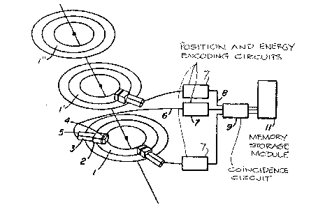
Fig. 1 ~s an overall block diagram of the apparatus.
Fig. 2 ~s an isometric ~iew of one crystal showing the light
absorbing band and orient~t~on ~n the array.
Fig. 3a is ~ diagrammatic, perspective view
illustrating a scintillation crystal optically coupled to
primary and secondary light sensing detectors.
Fig. 3b is a diagrammatic, perspective view of an
alternative embodiment o~ a scintillation crystal optically
coupled to primary and secondary light ~ensing de~ectors.
7 : ~
1~ [)3256
Fig. 4a, 4b and 4c are end, plan and side elevational
views, respectively, illustrating a crystal array coupled
to a multi-cathode photomuliplier as the primary light
sensing means and the top and bottom of the front sections
of the crystals coupled via light guides to secondary light
sensing detectors.
7a
,
~30~32~
Fig. 5 shows the advantage of the invention in reducing the
width of the coincidence aperture functions.
Fig. 6 shows a response function with and without the band
around the crystal.
Descriiption of the Preferred Embodîment
Referring now to Fig. 1 there is shown a series of rings 1,
1', 1" etc. each ring mutually disposed about a common axis. Each
ring is comprised of a plurality of discrete detector modules
containing one or more crystal detectors 2, a primary light
sensing means 3, means of coupling the light from the front of
each crystal 4, to the auxiliary light sensing means 5,
Electrical signals from the primary and secondary light sensing
means are coupled via cables 6, to amplifiers and position and
energy encoding circuits 7. When an event has been encoded, and
its energy determined to correspond with an un-scattered
annihilation photon a coded signal is sent over further cables 8,
to a coincidence circuit 9. If the coincidence circuit receives
signals from exactly two, non adjacent, detector modules within a
short time (a few nanoseconds), the addresses of each end of each
crystal are used to determine and address to increment in a memory
storage module 11. lhe contents of the storage memory are read out
from time to time and are processed by conventional image
reconstruction techniques. The essential distinction between this
and conventional imaging systems is that depth of interaction in
each crystal is provided as part of the coded address of each
event.
~L3~32~;6
Referring now to Fig. 2 which shows one of the discrete
crystals 2, which is generally in the form of a right rectangular
prism. The radiation enters through the front face 20, of the
crystal which is disposed near the surface of a hollow cylinder
which surrounds the patient section being scanned. The rear face
of the crystal 21, is optically coupled to the primary light
sensing means. The surfaces not in contact with light sensors ane
either highly polished or etched and covered with a highly
reflecting white substance. The light absorbing band 22, is
located near the equi-probable point of interaction 23, from the
front face. It can either be etched on the surface of a polished
crystal (to eliminate total internal reflection which normally
takes place at the crystal-air interface), or rendered black to
absorb l~ght which would have escaped via refractlon from the
crystal~ and would normally be reflected back from the white
material or paint on the crystal faces~ Note because of the
exponential attenuation of radiation within the crystal the
distance 23, is always less than half the length of the length of
the crystal. The face 24 is coupled to the secondary light sens;ng
means. The crystals are disposed in the rings such that the line
25, joining opposite corners of the crystal is directed towards
the~centre of the cylinder in order to provide spatially distinct
samples from front and rear sections of the crystal. The front
face may be cut slightly skewed to the other faces in order to
,;
,
~ ' .
~ao32s6
prevent the light from reflecting endlessly from the highly
polished faces of the crystal due to total internal reflection.
Referring now to Fig. 3 which shows the disposition of the
light detecting means. Fig. 3a shows one of severai crystals 2,
coupled through an optional light guide 31, to a multiple cathode
photomultiplier as the primary light sensing means 3. In one
embodimert a high gain, low noise, semiconducting photo diode 32,
coupled to crystal face 24, is used as the secondary light sensing
means. In an alternative embodiment, shown in Fig. 3b a light pipe
33 couples the light from crystal face 24, to a common single
element photomultiplier 34, to which the front ends of all
crystals in the module would also be coupled. Depending on the
position encoding scheme employed, the crystals may be coupled to
the primary light sensing means through an optional light guide 31
whose purpose ls to diffuse the light and assist in the crystal
identification. In both of these embodiments the primary light
sensing photomultiplier provldes timing, energy and crystal
identification (using coding schemes already known to those
skilled in the art), the secondary light sensing means provides a
binary (front, back) decision to identify the region of each
,,
crystal, and may also be used to alter parameters used in the
coding scheme of the primary photo multiplier.
.,
Minor modifications of this such as the use of a plurality of ~
; ,
primary photomultipliers rather than one multi anode one as drawn
. . .
10 ^.,
.
~;~"~
13032~i6
here could be employed with a reduction of overall compactness,
and greater extent of dead zones due the adjacent glass enve10pes
in the inner walls of the photomultipliers.
Referring now to fig. 4 in which another possible embodiment
is shown in frontal elevation Fig. 4a, p1an elevation fig. 4b, and
side elevation fig. 4c. Here the crystals 2 are subdivided by a
horizontal lengthwise cut into two vertically disposed units 40,
41 coup1ed to the same primary photomult~plier 3. Light guides
41,42... 47 couple each crystal in the upper row to a secondary
photomultipl~er 5 while further light guides 41', 42'..43'..47'
couple each crystal in the lower row to a secondary
photomultiplier 5'.
Referring now to fig. 5 which shows the coincidence aperture
funckions wh~ch can be measured by a moving a point source of
positron emitting isotope in the plane o~ the detectors and
observing the number of coincident events recorded by all pairs of
crystals. Crystals 501 and 502 are diametrically opposed. Their
response 503 is not effected by penetration of the gamma rays.
Crystals 504 and 505 respond to events near the edge of the field
of view. The response 506, is blurred since many gamma rays
recorded by them have~passed through neighboring crystals without
being absorbed. Cry~;tals 520 and 521 are divided in~o
regions 507, 508 and 509, 510, respectively, along the
plane of equi-probable interaction. There are four
aperture ~unctions with equal area:~;, S11 from coincidences
between region~ 507 and
11
.~J"~
~L30~2~;6
509, 512 from coincidences between regions 507 and 510, 513
from coincidenceq between regions 508 and 509, and 514 from
coincidences between region~ 508 and 510. The sum of the
integrals of 511, 512, 513, and 514 is equal to 506, ~o the
efficiency is the ~ame, but the width~ of the former are
much narrower, improving ~patial resolution at the edg~ of
~he f 7 ~ld of view.
The following advantages are made with regard to this invention:
I0 The single discrete crystals of a dense material like bismuth
germanate can be made relatively deep to improve sensitivity while
preventing image blurring at the edge of the field of view.
A simple inexpensive means is employed to identify whether
the gamma ray interacts with the front or rear section of the
crystal using a light absorbing bahd and secondary light sensing
means.
The light absorbing band divides the crystal into two regions
such that a gamma ray is equally likely to interact with the
crystal in front of or behind the band. It follows that coincident
events involving a pair of these crystals wi11 divide into four
equi-probable groups. Previous schemes which propose detectors
made out different scinti11ators glued together and electronic
pulse shape discrimination do not give this event distribution.
Since the noise ~n the final image is due to ~he regions where the.
12
- ~- --, ....
~303~56 ~
counting statistics are poorest, separation into equi-probable
interaction regions will reduce image noise. Since all other
scintillators currently known are less dense than bismuth
germinates it follows that using a multi-element crystal will
result in reduced efficiency if the overall crystal depth is
constant, or increased resolution blurring if the crystals are
made deeper to retain efficiency.
.
Other embodiments falling within the lines of the appended
claims will occur to those skilled,in the art.
1 2 a
.
.
.