Note: Descriptions are shown in the official language in which they were submitted.
~3~3~
LIGHT RECEIVING ME~ER FOR USE
IN ELECTROPHOTOGRAPHY
FIELD OF THE INVENTION
This invention relates to an improved light receiving
member for use in electrophotography which is sensitive
to electromagn~tic waves such as light ~which herein means
in a broader sense.those lights such as ultra-violet rays,
visible rays, infrared rays, X-rays and y-rays).
. BACKGROUND OF THE INVENTION
For the photoconductive material to constitute a light
receiving layer in a.light receiving member for use in
electrop~oto~raphy, it is required to be highly senaitive,
to have a high SN ratio Ephotocurrent (Ip~/dark current (Id)],
to have absorpt~bn spectrum characteristi.cs suited:for the
spectrum characterlstics of an electromagnetic wave to be
irradlated, to be quiakly responsive and to have a desired
dark resistanceO It i~s also required to be not har~ful to
livin~ things as well as man upon the use.
Especially, in the case where it is the light receiving
member to be applied ln an.electrophotographic machine for
use in ofice, causing no pollution is indeed important~
~3'~:~3~8
From these standpoints, the public attention has been
focused on light receiving members comprising amorphous
materials containing silicon atoms (hereinafter referred
to as "a-Si"), for example, as disclosed in Offenlegungsschriftes
Nos. 2746967 and 2855718 which disclose use oE the light
receiving member as an image-forming member in electro-
photography.
For the conventional light receiving members comprising
a-Si materials, there have been made improvements in their
optical, electric and photoconductive characteristics such
as dark resistance, photosensitivity, and photoresponsiveness,
use-environmental characteristics, economic stability and
durability.
However, there are still left subjects to make further
improvements in their characteristics in the synthesis
situation in order to make such light receiving member
practically usable.
For example, in the case where such conventional light
receiving member is employed in the light receiving member
for use in electrophotography with aiming at heightening the
photosensitivity and dark resistance, there are often observed
a residual voltage on the conventional light receiving
member upon the use, and when it is repeatedly used for a
long period of time, fatigues due to the repeated use will
be accumulated to cause the so-called ghost phenomena
~1 ~'f1'-)~If~'~
inviting residual images.
~ urther, in the preparation oE the light receiving
layer of the conventional light receiving member for use
in electrophotography using an a-Si material, hydrogen atoms,
halogen atoms such as fluorine atoms or chlorine atoms,
elements for controlling the electrical conduction type such
as boron atoms or phosphorus atoms, or other kinds of atoms
for improving the characteristics are selectively incorporated
in the light receiving layer.
~ owever, the resulting light receiving layer sometimes
becomes accompanied with defects on the electrical character-
istics, photoconductive characteristics and/or breakdown
voltage according to the way of the incorporation of said
constituents to be employed.
That is, in the case of using the light receiving member
having such light receiving layer, the life of a photocarrier
generated in the layer with the irradiation of light is not
sufficient, the inhibition of a charge injection from the
side of the substrate in a dark layer region is not sufficiently
carried out, and image defects likely due to a local break- -
down phenomenon which is so-called "white oval marks on
half-tone copies" or other image defects likely due to
abrasion upon using a blade for the cleaning which is
so-called "white line" are apt to appear on the transferred
images on a paper sheet.
~3~
Further, in the case where the above light receiving
member is used in a much moist at~osphere, or in the case
where after being placed in that atmosphere it is used,
the so-called "image flow" sometimes appears on the
transferred images on a paper sheet.
In consequence, it is necessitated not only to make
a further improvement in an a-Si material itself but also to
establish such a light receiving member not to invite any of
the foregoing problems.
,
SU~ARY OF THE I~VENTION
The object of this invention is to provide a light
receiving member for use in electrophotography which has
a light receiving layer mainly composed of a-Si, free from
the foregoing problens and capable of satisfying various
kind of requirements in electrophotography.
That is, the main object of this invention is to
provide a light receiving member for use in electrophotography
which has a light receiving layer ormed of a-Si, that
electrical, optical and photoconductive properties are always
substantially stable scarcely depending on the wor~ing
circumstances, and that is excellent against optical fatigue,
causes no degradation upon repeating use, excellent in
durability`and moisture-proofness and exhibits no or scarce
~3~3~
residual voltaye.
~ nother object of this invention is to provide a light
receiving member for use in electrophotography which has
light receiving layer formed of a-Si which is excellent in
the close bondability with a substrate on which the layer
is disposed or between each of the laminated layers, dense
and stable in view of the structural arrangement and is of
high quality.
A further object of this invention is to provide a
light receiving member for use in electrophotography which
has a light receiving layer formed of a-Si which exhibits
a sufficient charge-maintaining function in the electrifi-
.
cation process of forming electrostatic latent images andexcellent electrophotographic characteristics when it is
used in electrophotographic method.
A still further object of this :invention is to provide
a light receiving member ~or use in electrophotography which
has a light receiving layer formed of a-Si which invites
neither an image defect nor an image flow on the resulting
visible images on a paper sheet upon repeated use in a long
period of time and which gives highly resolved visible images
with clearer half-tone which are highly dense and quality.
Other object of this invention is to provide a light
receiving member for use in electrophotography which has a
light receiving layer formed of a-Si which has a high
~3~ 6~3
photosensitivity, high S/N ratio and high electrical voltage
withstanding property.
The present inventors have made earnest studies for
overcoming the foregoing problems on the conventional light
receiving members for use in electrophotography and attain-
ing the objects as described above and, as a result, has
accomplished this invention based on the finding as described
below.
That is, in order to overcome the foregoing problems
on the conventional]ight receiving member for use in electro-
photography and attaining the above-mentioned objects, the
present in~entors have made varlous studies while forcusing
on its surface layer. As a result, the present inventors
have found that when the surface layer is formed of an
amorphous material containing silicon atoms, carbon atoms
and hydrogen atoms and the content of the hydrogen atoms is
controlled to be ranging in the range between 41 and 70
atomic %, those problems on the conventional light receiving
member ~or use in electrophotography can be satisfactorily
eliminated and the above-mentioned objects can be effectively
attained.
Accordingly, this invention is to provide a light
receiving member for use in electrophotography basically
comprising a su~strate usable for electrophotography, a light
receiving layer comprising a charge in~ection inhibition
~3~
layer being formed of an amorphous material containing
silicon atoms as the main constituent atoms and an element
for controlling the conductivity, a photoconductive laye.r
being formed of an amorphous material containing silicon
atoms as the main constitllent atoms and at least one kind
selected from hydrogen atoms and halogen atoms [hereinafter
referred to as "A-Si(H/X)"], and a surface layer having a
free surface being formed of an amorphous material containing
silicon atoms, carbon atoms and hydrogen atoms (hereinafter
referred to as l'A-Si:C:H"~ in which the amount of the
hydrogen atoms to be contained is ranging from ~1 to 70
atomic %.
. ,It is possible for the light receiving member according
to this invention to.have.an absorption layer for li~ht of
long wavelength (hereinafter re~erred to as "IR layer")
being formed of an amor~hous material containing silicon
atoms an~ germanium atoms, and if necessary, at least either
hydrogen atoms or halogen atoms lhereinafter referred to as
"~-SiGe (H,X)"] between the substrate and the ~harge injection
inhibition layer.
It is also possible for the light receiving member
according to this invention to have a contact layer formed
of an amorphous material containing silicon atoms and at
least one kind selected from nitrogen atoms, oxygen atoms
and carbon atoms,-and if necessary, at least either hydrogen
~3~3~
atoms or halogen atoms [hereinafter referred to as "A-Si
(N,O,C)(H,~)"] between the substrate and the IR layer or
between the substrate and the charge injection inhibition
layer.
~ nd, the above-mentioned photoconductive layer may
contain oxygen atoms or/and nitrogen atoms. The above-
mentioned charge injection inhibition layer is 50
structured that it contains the element for controlling the
conductivity as the layer constituent either in the state
of being distributed uniformly in the thicknesswise direction
or in the state of being disiributed largely in the local
layer region near the substrate. Further, the charge injection
inhibition layer may contain at least one kind selec~ed:
from nitrogen atoms, oxygen atoms and carbon atoms as the
constituent atoms either in the state of being distributed
uniformly in the thicknesswise direction or in the state
of being distributed largely-in the local layer region near
the substrate.
The above~mentioned IR layer may contain at least one
kind.selected from nitrogen atoms, oxygen atoms, carbon
atoms, and an element for controlling the conductivity
as the layer constituent.
The light receiving.member having the above-me~tioned
light receivins layer for use in electrophotography according
to this invention is free from the foregoing problems on the
~3~ 3~
conventional light receiving members for use in electro-
photography, has a wealth of practically applicable
excellent electric, optical and phtoconductive character-
istics and is accompanied with an excellent durability and
satisfactory use environmental characteristics.
Particularly~ the light receiving member for use in
electrophotography according to this invention has substan-
tially stable electric characteristics without depending
on the working circumstances, mai.ntains a high photosensi-
tivity and a high S/~ ratio and does not invite any
undesirable influence due to residual voltage even when it
is repeatedly used for along period of time. In addition,
it has sufficient mo~u;re registant and optical fat.igue
resistance, and ca~ neither degradation upon repeating
use nor any defect on breakdown voltage.
Because of this, according to the light receiving
member for use in electrophotography of this invention,
:even upon repeated use for a long period of time, highly
resolved visible images with clearer half tone which are
highly dense and quality are stably obtained,
BRIEF DESCRIPTION OF THE DRA~INGS
Figure, l(A) through Figure l(D) are schematic views
il.lustrating the typical layer constitution of a representative
13~3~
light receivin~ member for use in electrophotography
according to this invention ;
Figure 2 through Figure 7 are views illustrating the
thicknesswise distribution of germaniurn atoms in the IR
layer ;
Figure. 8 through Figure 12 are views illustrating the
thicknesswise distribution of the group III atoms or the
group V atoms in the charge injection inhibition layer;
Figure: 13 through Figure 19 are views illustrating the
thicknesswise distribution of at least one kind selected from
nitrogen atoms, oxygen atoms, and carbon atoms in the charge
injection inhibition layer.;
Figure:~ 20(A) through Figure 20(C) are schematic views
for examples of the shape at the surface of the substrate in
the light receiving member for use in electrophotography
according to this invention ;
Figure 21 is a schematic view for a preferred example
of the light receiving member for use in electrophotography
according to this invention which has a light receiving layer
as shown in Figure l(C) formed on the substrate having a
preferred surface ;
Figures 22 through 23 are schematic explanatory views
of a preferred method for preparing the substrate having the
preferred surface used in the light receiving member shown
in Figure 21 ;
~3U391~3
Figure 24 is a schematic explanatory view of a fabrica-
tion apparatus ~or preparing the light receiving member for
use in electrophotography according to this invention;
Figure 25 and Figure 26 are schematic views respectively
illustrating the shape of the surface of the substrate in
the light receiving member in Examples 7, 17 and 28, and
Examples 8, 18 and 29;
Figure 27 is a view illustrating the thicknesswise
distribution of boron atoms and oxygen atoms in the charge
injection inhibition layer in Example 2; and
Figure 28 is a view illustrating the thicknessw1se
distribution of boron atoms and oxygen atoms in the charge
injection inhibition layer and germanium atoms in IR layer
in Example 10 and 20.
DETAILED DESCRIPTION OF THE INVENTION
Representative embodiments of the light receiving
member for use in electrophotography according to this
invention will now be explained more specifically refer-
ring to the drawings. The description is not intended to
limit the scope of this invention.
Representative light receiving members foruse in
el~ctrophotography according to this invention are as shown
in Figure l(A) through Figure l(D), in which are shown
3~3~3~
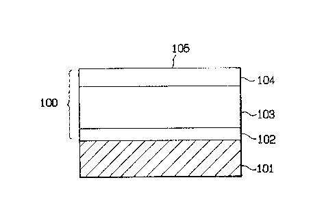
light receiving layer 100, substrate 101, charge injection
inhibition layer 102, photoconductive layer 103, surface
layer 104, free surface 105, IR layer 106, and contact
layer 107.
Figure l(A) is a schematic view illustrating a typical
representative layer constituion of this invention, in
which is shown the light receiving member comprising the
substrate 101 and the light receiving layer 100 constituted
by the charge injection inhibition layer 102, the photo-
conductive layer 103 and the surface layer 104.
Figure l(B) is a schematic view illustrating another
representative layer constitution of this invention, in
which is sho~n the light receiving member comprising the
substrate 101 and the light receiving layer 100 constituted
~y the IR layer 106, the charge .injection inhibition layer
102, the photoconductive layer 103 and the surface layer 104
Figure l(C) is a schematic view illustrating another
represntative layer constitu~i~n of this invention, in which
is shown the light receiving member comprising the substrate
101 and the light receiving layer 100 constituted by the
contact layer 107, the IR layer 106, the charge injection
inhibition layPr 102, the photoconductive layer 103 and
the surface layer 104.
Figure l(D) is a schematic view illustrating another
representative layer constitution of this invention, in
~3~13~
which is shown the light receiving member comprising the
substrate lOl and the light receiving layer constituted by
the contact layer 107, the charge injection inhibition layer
102, the photoconductive layer 103 and the surface layer 104
Now, explanation will be made for the substrate and
each constituent layer in the light receiving mem~er of
this invention.
Substrate 101
The substrate 101 for use in this invention may either
beelectn~conductive or insulative. The electroconductive
sùpport can include, for example, metals such as NiCr,
stainless steels, Al, Cr, Mo, Au, Nb, Ta, V, Ti, Pt and Pb
or the alloys thereof.
The electrically insulative support can include, for
example, films or sheets of synthetic resins such as
polyester, polyethylene, polycarbonate, cellulose acetate,
polypropylene, polyvinyl chloride, polyvinyli~ene chloride,
polystyrene, and polyamide, glass, ceramic and paper. It
is preferred that the electrically insulative substrate is
applied with electroconductive treatment to at least one o
the surfaces thereof and disposed with a light receiving
layer on the thus treated surface.
In the case of glass, for instance, electroconductivity
is applied by disposing, at the surface thereof, a thin
~lL3~3~
film made of NiCr, Al, Cr, r~o, Au, Ir, Nb, Ta, V, Ti, Pt,
Pd, In203, SnO2, ITO (In203 + SnO2), etc. In the case of
the synthetic resin film such as a polyester film, the
electroconductivity is provided to the surface by disposing
a thin film of metal such as NiCr, Al, Ag, Pv, Zn, Ni, Au~
Cr, Mo, Ir, Nb, Ta, V, Tl and Pt by means of vacuum
deposition, electron beam vapor deposition, sputtering,
etc., or applying lamination with the metal to the surface.
The substrate may be of any configuration such as cylindrical,
belt-like or plate-like shape, which can be properly determined
depending on the application uses. For instance, in the
case of using the light receiving member sho~m in Figure 1
in continuous high speed reproduction, it is desirably
configurated into an endless belt or cylindrical form.
The thickness of the support me~er is properly
determined so that the light receiv~g member as desired can
be formed.
In the case where flexibility is required for the light
receiving member, it can be made as thin as possible ~ithin
a range capable of sufficiently providing the func-tion as
the substrate. However, the thickness is usually greater
than 10 ~m in view of the fabrication and handling or mechanical
strength of the substrate.
And, it is possible for the surface of the substrate
to be uneven in order to eliminate occurrence of defective
14
.
3L3~3~8
images caused by a so-called interference fringe pattern
being apt to appear in the formed images in the case where
the image formation is carried out using coherent mono-
chromatic light such as laser beams.
In that case, the uneven surface shape of the substrate
can be formed by the grinding wor~ with means of an
appropriate cuttin~ tool, for example, havin~ a V-form bite.
That is, said cutting tool-is firstly fixed to the
predetermined position of milling machine or lathe, then,
for example, a cylindrical substrate i5 moved regularly in
the predetermined direction while being rotated in accordance
with the predetermined program to thereby obtain a surface-
treated cylindrical substrate of a surface having irregular-
ities in reverse V-form with a desirably pitch and depth.
The irreyularities thus formed at the surface of the
cylindrical substrate form a helical structure along the
-center axis of the cylindrical substratea The helical structure
making the reverse V-~orm irregularities or the surface of
the cylindrical substrate may be double or treble. Or
otherwise, it may be of a cross-helical structure.
Further, the irregularities at the surface of the
cylindrical substrate may be composed of said helical
structure and a delay line formed along the center axis of
the cylindrical substrate. The cross-sectional form of the
convex of the irregularity formed at the substrate surface
~L3~3~
is in a reverse V-form in order to attain controlled uneven-
ne~s of the layer thickness in the minute column for each
layer to be formed and secure desired close bondability
and electric contact between the substrate and the layer
formed directly ~hereon.
And it is desirable for the reverse V-form to be an
equilateral triangle; right-angled triangle or inequilateral
triangle~ Among these triangle forms, equilateral triangle
form and riht-angled triangle form are most preferred.
Each dimension of the irregularities to be formed
at the substrate surface under the controlled condltions is
properly determined having a due regard on the following
points.
That is, firstly, a layer composed of a-Si(H,X) to
constitute a light receiving layer is structurally sensitive
to the surface state of the layer to be formed and the layer
quality is apt to largely change in accordance wit the
surface state.
Therefore, it is necessary for the dimention of the
irregularity to be formed at the substrate surface to be
determined not to invite any decrease in the layer quality
of the layer composed of a Si(~I,X).
Secondly, should there exist extreme irregularities
on the free surface of the light receiving layer, cleaning
in the cleaning process after the formation of visible images
~3~
becomes difficult to sufflciently carry out. In addition,
in the case of carrying out the cleaning with a blade,
the blade will be soon damaged.
From the viewpoints of avoiding the problems
in the layer formation and the electrophotographic processes,
and from the conditions to prevent occurrence of the problems
due to interference fringe patterns, the pitch of the
irregularity to be formed at the substrate surface is
preferably 0.3 to 500 ~m, more preferably 1.0 to 200~mj and,
most preferably, 5.0 to 50 ~m.
As for the maximum depth of the irregularity, it is
preferably 0.1 to 5.0 ~m, more preferably 0.3 to 3.0 ~m,
and, most preferably, 0.6 to 2.0 ~m.
And when the pitch and the depth of the irregularity
lie respectively in the above-mentioned range, the inclina-
tion of the slope of the dent (or the linear convex) of the
irregularity is preferably 1 to 20, more preferably 3 to
15, and, most preferably, 4 to 10.
Further, as for the maximum figure of a thickness
difference based on the ununiformity in the layer thickness
of each layer to be formed on such substrate surface, in
the meaning within~the same pitch, it is preferably 0.1 to
2.0 ~m, more preferably 0.1 to 1.5 ~m, and, most preferably,
0.2 ~m to 1.0 ~m.
In alternative, the irregularity at the substrate
~3~
surface may be composed of a plurality of fine spherical
dimples which are more effective in eliminating the occur~
rence of defective images caused by the interference
fringe patterns especially in the case of using coherent
monochromatic light such as laser beams.
In that case, the scale of each of the irregu:Larities
composed of a plurality of fine spherical dimples is smaller
than the resolving power required for the light receiving
member for use in electrophotography.
A typical method of forming the irregularities composed
of a plurality of fine spherical dimples at the substrate
surface will be hereunder explained referrlng to Figures
22 and 23.
Figure 22 is a schematic view for a typical example
of the shape at the surface of the substrate in the light
receiving member for use in electrophotography according
to this invention, in which a portion of the uneven shape
is enlarged. In Figure 22, are shown a support 2201, a
support surface 2202, a rigid true sphere 2203, and a
spherical dimple 220~.
Figure 22 also shows an example of the preferred methods
of preparing the surface shape as mentioned above. That
is, the rigid true sphere 2203 is caused to fall gravitationally
from a position at a predetermined height above the substrate
surface 2202 and collide against the substrate surface 2202
18
~3~J3~
to thereby form the spherical d~mple 2204. A plurality of
fine spherical dimples 2204 each substantially of an identical
radius of curvature R and of an identical width D can be
formed to the substrate surface 2202 by causing a plurality
of rigid true spheres 2203 substantially of an identical
diameter R' to fall from identical height h simultaneously
or sequentially.
Figure 23 shows a typical embodiment of a substrate
formed with the uneven shape composed of a plurality of
spherical dimples at the surface as described above.
In the embodiment shown in Figure 23, a plurality of
dimples pits 2304, 2304 ... substantially of an identical
radius of curvature and substantially of an identical width
are formed while being closely overlapped with each other
thereby forming an uneven shape regularly by causing to fall
a plurality of spheres 2303, 2303, ... regularly and
substantially from an identical height.to different positions
at the surface 2302 of the support 2301. In this case, it
is naturally required for forming the dimples 2304, 2304 ...
overlapped with each other that the spheres 2303, 2303 ...
are graviationally dropped such that the times of collision
of the respective spheres 2303 to the support 2302 and
displaced from each other.
By the way, the radius of curvature R and the width D
of the uneven shape formed by the spherical dimples at the
19
~3~34C~3
substrate surface of the light receiving member fur use in
electrophotography according to this invention constitute
an important factor for effectively attaining the advantageous
effect of preventing occurrence o~ the interference fringe
in the light receiving member for use in electrophotography
according to this invention. The present inventors carried
out various experiments and, as a result, found the following
facts.
That is, if the radius of curvature R and the width D
satisfy the following equation:
D ~ 0 035
0.5 or more Newton rings due to the sharing interference are
present in each of the dimples. Further, if they satisfy
the following equation:
R - 0 055
one or more Newton rings due to the sharing interference
are present in each o~ the dimples.
From the foregoing, it is preferred that the ratio D/R
is greater than 0.035 and, preferably, greatar than 0.055
for dispersing the interference fringas resulted throughout
the light receiving member in each of the dimples thereby
preventing occurrence of the interference fringe in the
light receiving member.
Further, it is desired that the width D of the unevenness
~3~1`3~
formed by the scraped dimle is about 500 ~m at the maximum,
preferably, less than 200 ~m and, more preferably less than
100 ~m.
Figure 21 is a schematic view illustrating a represen-
tative embodiment of the li~ht receving member in which
i.s shown the light receiving member comprising the above-
mentioned substrate and the llght receiving layer 100
constituted by contact layer 2107, IR layer 2106, charge
injection inhibition layer 2102, photoconductive layer 2103,
and surface layer 2104 having free surface 2105.
Contact Layer 107 (or 2107)
.-The contact layer 107 (or 2107) of this invention is
formed of an amorphous material containing silicon atoms,
at least one kind selected nitro~en atoms, oxygen atoms and
carbon atoms, and i~ necessary, hydro~en atoms or/and
halogen ato~s.
Further, the contact layer ~ay contain an element for
controlling conductivity.
The main object of disposing the contact layer in the
light receiving member of this invention is to enchance the
bondability between the substrate and the charge injection
inhibition layer or between the substrate and the IR layer.
And, when the element for controlling the conductivity is
incorporated in the contact layer, the transportation of
13~
a charge between the substrate and the charge injection
inhibition layer is ef~ectively improved.
For incorporating various atoms in the contact layer t
that is, at least one kind selected from nitrogen atoms,
axygen atoms and carbon atoms; elements for controlling the
conductivity in case where necessary; they may be deistributed
either uniformly in the entire layer region or unevenly
in the direction toward its layer thickness.
In the light receiving member of this invention, the
amount of nitrogen atoms, oxygen atoms, or carbon atoms to be
incorpoxated in the contact layer is properly determined
according to use purposes.
It is preferably 5 x 10 to 7 xlO atomic %, more
preferably 1 x 10 to 5 x 10 atomic %, and, most preferably,
2 x 10 3 to 3 x 10 atomic %.
For the thickness of the contact layer, it is properly
determined having a due regard to its bondability, charge
transporting af~iciency, and also to its producibility.
It is pre~erably 1 x 10 2 to i x 10 ~m, and, most
preferably, 2 x 10 2 to 5 ~m.
As for the hydrogen atoms and halogen atoms to be
optionally incorporated in the contact layer, the amount
of hydrogen atoms or halogen atoms, or the sum of the
amount of hydrogen atoms and the amount of halogen atoms
in the contact layer is preferably 1 x 10 to 7 x 10 atomic %,
~3~3~
more preferably 5 x 10 l to 5 x 10 atomic ~, and, most
preferably, l to 3 x lO atomic ~.
IR Layer 106 (or 2106)
In the light receiving member for use in eleckrophoto-
graphy of this invention, -the I~ layer is formed of A-SiGe
(H,X), and it is disposed directly on the above-mentioned
substrate or on the above-mentioned contact layer.
~ s for the germanium atoms to be contained in the IR
layer, they may be distributed uniformly in its entire
layer region or unevenly in the direction toward the layer
thickness of its entire layer region.
But in any case, it is necessary for the germanium atoms
to be distributed uniformly in the direction parallel to
the surface of the substrate in order to provide the
uni~ormness of the characteristics to be brought out.
(Herein or hereinafter, the uniform distribution means
that the distribution of germanium atoms in the layer is
unlform both in the dlrection parallel to the surface of the
substrate and in the khickness direction. The uneven distribu-
tion means that the distribution of germanium atoms in the
~layer is uniform in the direction parallel to the surface of
the substrate but is uneven in the thickness direction.)
That is, in the case in where the germanium atoms
contained unevenly in the direction toward the layer thickness
~3~34~8
of its entire layer region, the germanium atoms are
incorporated so as to be in the state that these atoms are
more largely distributed in the layer region near the
substrate than in the layer apart from the substrate (namely
in the layer region near the free surface of the light
receiving layer) or in the state opposite to the abo~e state.
In preferred embodiments, the germanium atoms are
contained unevenly in the direction toward the layer thickness
of the entire layer region of the IR layer.
In one of the preferred embodiments, the germanium atoms
are contained in such state that the distributing concentra-
tion of these atoms is changed in the way of being decreased
from the layer regîon near the substrate toward the layer
region near the charge injection inhibition layer. In this
case, the affinity between the IR layer and the charge
injection inhibition becomes excellent. And, as later
detailed, when the idstributing concentration of the germanium
atoms is made significantly large in the layer region adjacent
to the substrate, the IR layer becomes to substantially and
completely absorb the light of long wavelength that can
be hardly absorbed by the photoconductive layer in the case
of using a semiconductor laser as the light source. As a
result, the occurrence of the interference caused by the
light reflection from the surface of the substrate can be
effectively prevented.
~4
~3~3~
Explanation will be made to the typical embodiments
of the distribution of ge.rmanium atoms to be contained
unevenly in the direction toward the layer thickness of
the IR layer while referring to Figures 2 through 7 showing
the distribution of germanium atoms. However, this invention
is no way limited only to these embodiments.
In Figures 2 through 7, the abscissa represent the
distribution concentration C of germanium atoms and the
ordinate represents the thickness of the IR layer; and tB
represents the extreme position of the IR layer containing
germanium atoms is formed from the tB side toward the tT side.
Figure 2 shows the first typical example of the thickness-
wise distribution of the germanium atoms in the IR layer.
In this example, germanium atoms are distributed such that
the concentration C remains constant at a value Cl in the
range ~rom position tB ~at which the IR layer comes into
contact with the substrate) tG position tl, and the concen-
tration C gradually and continyously decreases from C2 in the
range from position tl to position tT~ where the concentration
of the germanium atoms is C3.
In the example shown in Figure 3, the distribution
concentration C of the germanium atoms contained in the IR
layer is such .that concentration C4 at position tB continuously
decreases to concentration C5 at position tT~
In the example shown in Figure 4, the distribution
~L3~ Q8
concentration C of the germanium atoms is such that the
concentration C6 remains constant in the range from
position tB and position t2 and it gradually and continyously
decreases in the range from position t2 and position tT.
The concentration at position tT is substantially zero.
("Substantially zero" means that the concentration is lower
than the detectable limit.)
In the example shown in Figure 5, the distribution
concentration C of the germanium atoms is such that concen-
tration C8 gradually and continuously decreases in the range
~rom position tB and position tT~ at which it is substantially
zero.
In the example shown in Figure 6, the distribution
concentratlon C of the germanium atoms is such that concen-
tration Cg remains constant in the range from position tB
to position t3, and concentration C9 linearly decreases to
concentration C10 in the range from position t3 to position t
In the example shown in Figure 7, the distribution
concentration C of the germanium atoms is such that concen-
tration Cll linearly decreases in the range from position tB
to position tT~ at which the concentration is substantially
zero.
Several examples of the thicknesswise distribution of
germanium atoms in the IR layer are illustrated in Figures
2 through 7 r In the light receiving member of this invention,
2~
~IL3~3~
the concentration (C) of germanium atoms in the IR layer
is preferred to be high at the position adjacent to the
substrate and considerably low at the position adjacent to
the interface tT.
The thickn~sswise distribution of germanium atoms
contained in the IR layer is such that the maximum concen-
tration Cmax of germanium atoms is preferably greater than
1 x 10³ atomic ppm, more preferably greater than 5 x 10³
. atomic ppm, and most preferably, greater than 1 x 10⁴ atomic
ppm based on the total a~ount of silicon atoms and germanium
atoms~
For the amount of germanium atoms to be contained in
the IR layer, it is properly determined according to desired
requirements. However, it is preferably 1 to 1 x 10⁶ atomic
ppm, more.preferably 102 to 9.5 x 10⁵ atomic ppm, and, most
preferably, 5 x 10² to 8 x 10⁵ atomic ppm based on the total
amount of silicon atoms and germanium atoms.
Further, the IR layer may contain at least one kind
selected from the element for controlling the conducti~ity,
nitrogen atoms, oxygen atoms and carbon atoms.
In that case, its amount is preferably 1 x 10² to
4 x 10 atomic %, more preferably 5 x 10 to 3 x 10 atomic %,
and most preferably 1 x 10 1 to 25 atomic %.
As for the element for controlling the conductivity,
so-called impurities in the field of the semi.conductor can
~3~
be men~ion-d and those usable herein can include atoms
belonging to the group III of the periodic table that
provide p-type conductivity (hereinafter simply referred
to as "group III atoms") or atoms belonging to the group V
of the periodic table that provide n-type conductivity
(hereinafter simply referred to as "group V atoms").
Specifically, the group III atoms can include B (boron),
Al (aluminum), Ga (gallium), In (indium) and Tl (thallium),
B and Ga being particularly preferred. The group ~ atoms
can include P (phosphorus), As (arsenic), Sb (antimony),
and Bi (bismuth), P and Sb being particularly preferred.
For the amount of the element for controlling the
conductivity, it is preferably 1 x 10 to 5 x 10⁵ atomic
ppm, more preferably 5 x 10 1 to 1 x 10⁴ atomic ppm, and,
most preferably, 1 to 5 x 10³ atomic ppm.
~nd as for the thickness of the IR layer, it is preferably
O O
30 A to 50 ~m, more preferably 40 A to 40 ~m, and, most
preferably, 50 A to 30 ~m.
Charge Injection Inhibition Layer 102
In the light receiving member for use in electrophotography
of this invention, the charge injection inhibition layer 102
is formèd of A-Si(H,X) containing the element for controlling
the conductivity uniformly in the entire layer region or
largely in the side of the substrate.
~3~3~(~1!3
And said layer may contain at least one kind selected
nitrogen atoms, oxygen atoms and carbon atoms in the state
of being distributed uniformly in the entire layer region
or partial layer region but largely in the side of the
substrate.
And the charge injection inhibition layer 102 is
disposed on the substrate 101, the IR layer 106, or the
contact layer 107.
The halogen atom (X) to be contained in the charge
injection inhibition layer include preferably F ~fluorine),
Cl (chlorine), Br (bromine), and I (iodine), F and Cl being
particularly preferred.
The amount of hydrogen atoms (H), the amount of the
hydrogen atoms (X) or the sum of the amounts for the hydrogen
atoms and the halogen atoms (~l+X) contained in the layer 102
is preferably 1 to 40 atomic ~, and, most preferably, 5 to 30
atomic ~.
As for the element for controlling the conductivity
to be contained in the layer 102, the group III or group V
atoms can be used likewise in the case of the above-mentioned
IR layr.
~ Explanation will be made to ~he typical embodiments
for distributing the group III atoms or group V atoms in
the direction toward the layer thickness in the charge
injection inhibition layer while referring to Figures 8
29
~L3~34(~3
through 12.
In Figures 8 through 12, the abscissa represents the
distribution concentration C o~ the group III atoms or
group V atoms and -the ordinate represents the thickness of
the charge injection ihibition layer; and tB represents
the extreme position of the layer adjacent to the substrate
and tT represents the other extreme position of the layer
which is away from the substrate.
The charge injection inhibit-on layer is formed from
the tB side toward the tT side.
Figure 2 shows the first typical example of the thickness-
wise distribution of the group III atoms or group V atoms
in the charge injection ihibition layer. In this example,
the group III atoms or group V atoms are distributed such
that the concentration C remains constant at a value Cl2
in the range from position tB to position t4, and the
concentration C qradually and continuously decreases from
C13 in the range from position t4 to position tT~ where the
concentration of the group III atoms or group V atoms is Cl4.
In the example shown in Figure 9, the distribution
concentration C of the group III atoms or group V atoms
contained in the light receiving layer is such that concen-
tration C15 at position tB continyously decreases to concen-
tration Cl6 at position tT.
In the example shown in Figure lO, the distribution
~3~34~3
concentration C of the group III atoms or group V atoms is
such that concentration C17 rema.ins constant in the range
from position tB to position t3, and concentration C17
linearly decreases to concentration C18 in the range from
position t5 to position tT~
In the example shown in Figure 11, the distribution
concentration C of the group III atoms or group V atoms is
such that concentration Clg remains constant in the range from
position tB and position t6 and it linearly decreases from
C20 to C21 in the range from position t6 to position tT~
In the example shown in Figure 12, the distribution
concentration C of the group III atoms or group V atoms is
such that concentration C22 remains constant in the range
from position tb and position tT~
In the case where the group III atoms or group V atoms
are contained in the charge injection inhibition layer in such
way that the distribution concentration of the atoms in the
direction of the layer thickness is higher in the layer
region near the substrate, the thicknesswi.se distribution
of the group III atoms or group V atoms is preferred to be
made inthe way that the maximum concentration of the group
III atoms or group V atoms is controlled to be preferably
greater than 50 atomic ppm, more preferably greater than 80
atomic ppm, and, most preferably, greater than 10 atomic ppm.
For the amount of the group III atoms or group V atoms
~3~34~
to be contained in the charge injection inhibition layer,
it is properly determined according to desired requirements.
However, it is preEerably 3 x 10 to 5 x 10⁵ atomic ppm, ~ore
preferably 5 x 10 to 1 x 10~ atomic ppm~ and, most preferably,
1 x 10² to 5 x 10³ atomic ppm.
When at least one kind selected from nitrogen atoms,
oxygen atoms and carbon atoms is incorporated in the
charge injection inhibition layer, the bondability between
the IR layer and the charge injection inhibition layer and
the bondability between the charge injection inhibition layer
and the photoconductive layer is effectively improved.
Explanation will be made to the typical embodiments
~or distributing at least one kind selected from nitorgen
atom, oxygen atoms and carbon atoms in the direction toward
the layer thickness in the charye injection inhibition layer,
with reference to Figures 13 through 19.
In Figures 13 through 19, the abscissa represents the
distribution concentration C of at least one kind selected
from nitrogen atoms, oxygen atoms and carbon atoms, and
the ordinate represents the thickness of the charge injection
inhibition layer; and tB represents the extreme position of
the layer ajacent to the substrate and tT represents the
other extreme position of the layer which is away from the
substrate. The charge injection inhibition layer is formed
from the tB side toward the tT side.
~3~3~8
Figure 13 shows the first typical example of the
thicknesswise distributi.on of at least one kind selected
from nitrogen atoms, oxygen atoms and carbon atoms in the
charge injec-tion inhi.bition layer. In this example, at
least one kind selected from nitrogen atoms~ oxygen atoms
and carbon atoms are distributed such that the concentration
C remains constant at a value C23 in the range from
position tB to position t7, and the concentration C gradually
and continyously decreases from C24 in the range from
position t7 to position tT/ where the concentration of
at least one kind selected from nitrogen atoms, oxygen atoms,
and carbon atoms is C25.
In the exa~ple shown in Figure 1.4, the distribution
concentration C of at least one kind selected from nitrogen
atoms, oxygen atoms, and carbon atoms contained in the
charge injection inhibition layer is such that concentra-
tion C26 at position tB continuously decreases to concen-
tration C27 at position tT~
In the example shown in Figure 15, the distribution
concentration C of at least one kind selected from nitrogen
atoms, oxygen atoms, and carbon atoms is such that concen-
tration C28 remains constant in the range from position tB
and position t8 and it.gradually and continyously decreases
from position t8 and becomes substantially zero between
t8 and tT.
~3~3~
In the example shown in Figure 16, the distribution
concentration C of at least one kind selected from nitrogen
atoms, oxygen atoms and carbon atoms is such that concen-
tration C30 gradually and continyously decreases from
position tB and becomes substantially zero between t~ and
tT .
In the example shown in Figure 17, khe distribution
concentration C of at least one kind selected from nitrogen
atims, oxygen atoms and carbon atoms is such that concen-
tration C31 remains constant in the range from position tB
to position tg/ and concentration Cg linearly decreases
to concentration C32 in the range from position tg to
position tT.
In the example shown in Figure 18~ the distribution
concentration C of at least one kind selected from nitrogen
atoms, oxygen atoms and carbon atoms is such that concen-
tration C33 remains constant in the range from position tB
and position tlo and it linearly decreases from C34 to
C3~ in the range from position tlo to position tT.
In the example shown in Figure 19, the distrlbution
concentration C o~ at least one kind salected from nitrogen
atoms, oxygen atoms and carbon atoms is such that concen-
tration C36 remains constant in the range from position tB
and posltion tT.
In the case where at least one kind selected from nitrogen
34
~L3~3~
atoms, oxygen atoms and carbon atoms is contained in the
charge injection inhibition layer such that the distri~ution
concentration of these atoms in the layer is higher in the
layer region near the substrate, the thicknesswise
distribution of at least one kind selected from nitrogen
atoms, oxygen atoms and carbon atoms is made in such way
that the maximum concentration of at least one kind selected
from nitrogen atoms, oxygen atoms and carbon atoms is
controlled to be preferably greater than 5 x 10 atomic ppm,
more preferably, greater than 8 x 10² atomic ppm, and, most
preferably, greater than 1 x 10³ atomic ppm.
As for the amount of at least one kind selected from
nitrogen atoms, oxygen atoms and carbon atoms is properly
determined according to desired requirements. However, it is
preferably 1 x 10 3 to 50 atomic %, more preferably, 2 x 10 3
atomic % to 40 atomic ~, and, most preferably, 3 x 10 3
to 30 atomic %.
For the thickness of the charge injection inhibition
layer, it is preferably 1 x 10 2 to 10 ~m, more preferably,
5 x 10 2 to 8 ~m, and, most preferably, 1 x 10 1 to 5 ~m
in the viewpoints of bringing about electrophotographic
characteristics and economical effects.
Photoconductive Layer 103 (or 2103)
The photoconductive layer 103 (or 2103) i5 disposed on
~L3~408
the substrate 101 (or 2102) as shown in Figure 1 (or
Figure 21).
The photoconductive layer is formed of an a~Si(H,X)
material or an a-Si(H,X)(O,N) material.
The photoconductive layer has the semiconductor
characteristics as under mentioned and shows a photo-
conductivity against irradiated light.
(i) p-type semiconductor characteristics : containing an
acceptor only or both the acceptor and a donor in
which the relative content of the acceptor is higher;
(ii) p-type semiconductor characteristics : the content of
the acceptor (Na) is lower or the relative content of
the acceptor i5 lower in the case (i);
(iii)n-type semiconductor characteristics : containing a
donor only or both the donor and an acceptor in which
the relative content of the donor is higher;
(iv) n-type semiconductor characteristics : the content of
donor (Nd) is lower or the relative content of the
acceptor is lower in the case (iii), and
(v) i-type semiconauctor characteristics :
Na~Nd ~0 or Na~ Nd.
- In order for the photoconductive layer to be a desirable
type selected from the above-mentioned types (i) to (v), it
can be carried out by doplng a p-type impurity, an n-type
impurity or both the impurity with the photoconductive
36
~L3~34~3
layer to be formed durin~ its forming process while control-
ling the amount of such impurity.
As the element to be such impurity to be contained
in the photoconductive layer, the so-called impurities in
the field of the semiconductor can be mentioned, and those
usable herein can include atoms belonging to the group III
or the periodical table that provide p-type conductivity
(hereinafter simply referred to as "group III atom") or
atoms belon~ing to the group V of the periodical table that
provide n-type conductivity (hereinafter simply referred
to as "group V atom"). Specifically, the group III atoms
ean include B (boron), Al (aluminum), Ga (gallium), In
(indium) and Tl (thallium). The group V atoms ean inelude,
for example, P (phosphor), As (arsenie), Sb (antimony) and
Bi (bismuth~. Among these elements, B, Ga, P and As are
partieuarly preEerred.
The amount of the group III atoms or the group V atoms
to be contained in-the photoeonduetive layer is preferably-
1 x 10³ to 3 x 10 atomie ppm, more preferably, 5 x 10³ to
1 x 10² atomie ppm, and, most preferably, 1 x 10² to 50
atomic ppm.
In the photoconductive layer, oxygen atoms or/and
nitrogen atoms ean be incorporated in the range as long as
the characteristics required for that layer is not hindered.
In the case of incorporating oxygen atoms or/and
37
~3~3~C~8
nitrogen atoms in the entire layer region of the photo-
conductive layer, its dark resistance and close bondability
with the substrate are improved.
The amount of oxygen atoms or/and nitrogen atoms to
be incorporated in the photoconductive layer is desired to
be relatively small not to deteriorate its photoconductivity.
In the case of incorporating nitrogen atoms in the
photoconductive layer, its photosensitivity in addition to
the above advantages may be impro~7Qd when nitrogen atoms
are contained together with boron atoms therein.
The amount of one kind selected from nitrogen atoms (N),
and oxygen atoms (O) or the sum of the amounts for two kinds
of these atoms to be contained in the photoconductive layer
is preferably 5 x 10 4 to 30 atomic %, more preferably,
1 x 10 2 to 20 atomic %, and, most preferably, 2 x 10 to
15 atomic %.
The amount of the hydrogen atoms (H), the amount of
the halogen atoms ~H) or the sum of the amounts for the
hydrogen atoms and the halogen atoms (H+X) to be incorporated
in the photoconductive layer is preferably 1 to 40 atomic %,
more preferably, 5 to 30 atomic ~.
The halogen atom (X) includes, specifically, fluorine,
chlorine, bromine and iodine. And among these halogen atoms,
fluorine and chlorine and particularly preferred.
The thickness of the photoconductive layer is an important
38
~L3f~
factor in order for the photocarriers generated by the
irradiation of liyht having desired spectrum characteristics
to be effectively transported, and it is appropriately
determined depending upon the desired purpose.
It is, however, also necessary that the layer thickness
be determined in view of relative and organic relationships
in accordance with the amounts of the halogen atoms and
hydrogen atoms contained in the layer or the characteristics
required in the relationship with the thickness of other
layer. Further, it should be determined also in economical
point ov view such as productivity or mass productivity.
In view of the above, the thickness of the photoconductive
layer is preferably 1 to 100 ~m, more preferably, 1 to 80 ~m,
and, most preferably, 2 to 50 ~m.
Surface Layer 104 (or 2104)
-
The surface layer 104 (or 2104) having the free surface
105 (or 2105~ is disposed on the photoconductive layer 103
(or 2103) to attain the objects chiefly of moisture resistance,
deterioration resistance upon repeating use, electrical
voltage withstanding property, use environmental character-
istrics and durability for the light receiving member for
use in electrophotography according to this invention.
The surface layer is formed of the amorphous material
containing silicon atoms as the constituent element which
39
~l3~34~1~
are also contained inthe layer constituent amorphous material
for the photoconductive layer, so that the chemical stability
at the interface between the two layers is sufficiently
secured.
Typicall, the surface layer is formed of an amorphous
material containing silicon atoms, carbon atoms, and hydrogen
atoms (hereinafter referred to as ''A-(SiXCl X)yHl y",
x>O and y<l).
It is necessary for the surface layer for the light
receiving member for use in electrophotography according
to this invention to be carefully formed in order for that
layer to bring about the characteristics as required.
That is, a material containing silicon atoms (Si),
carbon atoms (C) and hydrogen atoms (H) as the constituent
elements is structually extended from a crystalline state
to an amorphous state which exhibit electrophysically
.properties from conductiveness to semiconductiveness and
insulativeness, and other properties from photoconductive-
ness to in photoconductiveness according to the kind of
a material.
Therefore, in the formation of the surface layer,
aypropriate layer forming conditions are re~uired to be
strictly chosen under which a desired surface layer composed
of ~-SixCl x havi.ng the characteristics as required may be
effectively formed.
~3~3~
For instance, in the case of disposing the suxface
layer with aiming chiefly at improvements in its
electrieal voltage withstanding property, the surface layer
composed f A-(SixCl y)y : H1 y is so formed that it
exhibits a significant electrical insulative behavlor in
use environment.
In the case of disposing the surface layer with aiming
at improvements in repeating use characteristics and use
environmental characteristics, the surface layer composed
of A-SiXCl x is so formed that it has certain sensitivity
to irradiated light although the electrical insulative
property should be somewhat decreased.
The amount of carbon atoms and the amount of hydrogen
atoms respectively to be contained in the surface layer of
the -ight reeeiving member for use is electrophotography
according to this invention are important factors as well
as the surface layer forming conditions in order to make the
surface layer aeeompanied with desir~d eharaeteristics to
attain the objeets of this invention.
The amount of the earbon atoms (C) to be ineorporated
in the surface layer is preferably 1 x 10 3 to 90 atomic %,
and, most preferably~ 10 to 80 atomic % respectively to the
sum of the amount of the silicon atoms and the amount of
the carbon atoms.
The amount of the hydrogen atoms to be incorporated
41
13~3~
in the surface layer is preferably 41 to 70 atomic %, more
preferably 41 to 65 atomic ~, and, most preferably, 45 to
60 atomic % respectively to the sum of the amount of all
the constituent atoms to ~e incorporated in the surface
layer.
~ s long as the amount of the hydrogen atoms to be
incorporated in the surface layer lies in the above-mentioned
range, any of the resulting light receiving members for use
in electrophotography becomes wealthy in significantly
practically applicable characteristics and to excel the
conventional light receiving members for use in electro-
photography in every viewpoint.
. That is, for the conventional llght receiving member
fo~ use in electrophotography, that is known that when
there exist certain defects within the surface layer composed
of A-(SiXCl x)y Hl y (due to mainly dangling bonds of
silicon atoms and those of carbon atoms) they gi~e undesiable
influences to the electrophotographic characteristics.
For instance, becasue os such defects there are often
invited deterioration~in the electrification characteristics
-due to charge injection from the side of the free surface,
changes in the electrification characteristics due to altera
tions in the surface structure under certain use environment,
for example, high moisture atmosphere, and appearance of
residual images upon repeating use due to that an electric
42
:1 3~3~8
charge is injected into the surface layer from the photo-
conductive layer at the time of corona discharge or at
the time of light i~rradiation to thereby make the electric
charge trapped for the defects within the surface layer.
However, the above defects being present in the
surface layer of the conventional lïght receiving member
for use in electrophotography which invite various problems
as mentioned above can be largely eliminated by controlling
the amount of the hydrogen atoms to be incorporated in the
surface layer to be more than 41 atomic ~, and as a result,
the foregoing problems can be almost resolved. In addition,
the resulting light receiving member for use in electro-
photography becomes t- have extremely improved advantages
especially in the electric characteristics and the repeating
usability at high speed in comparison with the conventional
light receiving member for use in electrophotography.
And, the maximum amount of the hydrogen atoms to be
incorporated in the su-face layer is necessary to be 70 atomic
%. That is, when the amount of the hydrogen atoms exceeds
70 atomic`%, the hardness of the surface layer is undesirably
decreased so tha tht eresulting light receiving member
~ecomes such that can not be repeatedly used for along
period of time.
In this connection, it is an essential factor for the
light receiving member for use in electrophotography of
43
~3~3~
this invention that the surface layer contains the amount
of the hydrogen atoms ranging in the above-mentione range.
For the incorporation of the hydrogen atoms in said
particular amount in the surface layer, it can be carried
out by appropriately controlling the rela-ted conditions
such as the flow rate of a starting gaseous substance, the
temperature of a substrate, discharging power and the gas
pressure.
Specifically, in the case where the surface layer is
rmed of A (Sixcl_x)y Hl_y, the "x" is preferably 0 1
to 0.99999, more preferably 0.1 to 0.99, and, most
preferably, 0.15 to 0.9. And the "y" is preferably 0.3 to
0.59, more preferably 0.35 to 0~59, and, most preferably,
0.4 to 0.55.
The thickness of the surface layer in the light receiving
member according to this invention is appropriately
determined depending upon the desirecL purpose.
It is, however, also necessary that the layer thickness
be determined in view of relative a~d organic relationships
in accordance with the amounts of the halongen atoms,
hydrogen atoms and other kind atoms contained in the layer
or the characteristics required in the relationship with
the thickness of other layer. Further, it should be determined
also in economical point of view such as productivity or mass
productivity. In view of the above factors, the thickness
4~
~3~3~
of the surface layer is preferably 0.003 to 30 ~m, more
preferably, 0.00~ to 20 ~m, and, most preferably, 0.005
to 10 ~m.
~ y the way, the thickness of the light receiving layer
100 constituted by the photoconductive layer 103 (or 2103
in Figure 21) and the surface layer 10~ (or 2194 in Figure
21) in the light receiving member for use in electro-
photography according to this invention is appropriately
determined depending upon the desired purpose.
In any case, said thickness is appropriately determined
in view of relative and organic relationships between the
thickness of the photoconductive layer and that of the
surface layer so that the various desired characteristics
for each of the photoconductive layer and the surface layex
in the light receiving member for use in electrophotography
can be sufficiently brought about upon the use to effectively
attain the foregoing objects of this invention.
And, it is preferred that the thicknesses of the photo~
conductive layer and the surface layer be determined so that
the ratio of the former versus the latter lies in the
range of some hundred times to some thousand times.
Specifically, the thickness of the light receiving layer
100 is preferably 3 to 100 ~m, more preferably 5 to 70 ~m,
and, most preferably, 5 to 50 ~m.
~5
~3~
Preparation o~ Layers
The method of forming the light receiving layer 100
of the light receiving member will be now explained.
Each of the layers to be constitue the light receiving
layer of the light receiving member of this invention is
properly prepared by vacuum deposi-tion method utilizing
the discharge phenomena such as glow discharging, sputtering
and ion plating methods wherein relevant gaseous starting
materials are selectively used.
These production methods are properly used selectively
depending on the ~actors such as the manufacturing conditions,
the installation cost required, production scale and properties
required for the light receiving members to be prepared.
The glow discharging method or sputtering method is suitable
since the control for the condition upon preparing the light
receiving members having desired properties are relatively
easy, and hydrogen atoms, halogen atoms and other atoms can
be introduced easily together with silicon atoms. The glow
discharging method and the sputtering method may be used
together in one ir~entical system.
Preparation of Photoconductive Layer, Charge In]ection
Inhibition Layer, and Contact Layer
.
Basically, when a layer constituted with A-Si(H,X) is
formed, for ecample, by the glow discharging method, gaseous
~6
~3~3~
starting material capable o~ supplying silicon atoms (Si)
are introduced together with gaseous starting material for
introducing hydrogen atoms (H) and/or halogen atoms (X) into
a dep~sition chamber the inside pressure o~ which can be
reduced, glow discharge is generated in the deposition
chamber, and a layer composed of ~-Si(H,X) is formed on the
surface of a suhstrate placed in the deposition chamber.
The gaseous starting material for supplying Si can
include gaseous or gasifiable silicon hydrides (silanes)
4~ Si2H6~ Si3H8, Si4Hlo, etc., SiH4 and Si H
being particularly preferred in view of the easy layer forming
work and the good efficiency for the supply of Si.
Further, various halogen compounds can be mentioned as
the gaseous starting material for introducing the halogen
atoms, and gaseous or gasifiable halogen compounds, for example,
gaseous halogen, halides, inter-halogen compounds and halogen-
substituted silane derivatives are preferred. Specifically,
they can include halogen gas such as of fluorine, chlorine,
bromine, and iodine; inter-halogen compounds such as BrF,
ClF, ClF3, BrF2, BrF3, IF7, ICl, IBr, etc.; anA silicon
halides such as SiF~, Si2F6, SiC14, and SiBr4. The use of
the gaseous or ~asifiable silicon halide as described above
is particularly advantageous since the layer constituted with
halogen atom-containing ~-Si:H can be formed with no addition~l
use of ~he gaseous starting silicon hydride material for
47
~3q~
supplying Si.
In the case of forming a layer constituted with an
amorphous material containing halogen atoms, typically, a
mixture of a gaseous silicon ahlide substance as the
starting material for supplying Si and a gas such as Ar,
H2 and He is introduced into the deposition chamber having
a substrate in a predetermined mixing ratio and at a pre-
determined gas flow rate, and the thus introduced gases are
exposed to the action of glow discharge to thereby cause
a gas plasma resulting in forming said layer on the substrate.
And, for incorporating hydrogen atoms in said layer, an
appropriate gaseous starting material ~or supplying hydrogen
atoms can be additionally used.
Now, the gaseous starting material usable for supplyins
hydrogen atoms can include those gaseous or gasifiable
materials, for example, hydrogen gas (H2), halides such as HF,
HCl, HBr, and HI, silicon hydrides such as SiH4, Si2H6,
Si3H8, and Si4Hlo, or halogen-substituted silicon hydrides
such as SiH2F2, SiH2 2~ SiH2C 2~ HC 3~ 2 2' 3
The use of these gaseous starting material is advantageous
since the content of the hydrogen atoms (H), which are
extremely effective in view of the control for the electrical
or photoelectronic properties, can be controlled with ease.
Then, the use of the hydrogen halide or the halogen-substituted
silicon hydride as described above is particularly advantageous
48
~3~3~L~J ~
since the hydro~en atoms (H) are also introduced together
with the introduction of the halogen atoms.
The amount of the hydrogen atoms (H) and/or the amount
of the halogen atoms (X) to be contained in a layer are
adjusted properly by controlling related conditions, for
example, the temperature of a substrate, the amount o~ a
gaseous starting material copable of supplying the hydrogen
atoms or the halogen atoms into the deposition chamber and
the electric discharging power.
In the case of forming a layer composed of A-Si(H,X)
by the reactive sputtering process, the layer is formed on
the substrate by using an Si target and sputtering the Si
target in a plasma atmosphere.
To form said layer by the ion-plating process, the vapor
of silicon is allowed to pass through a desired.gas plasma
atmosphere. The silicon vapor is produced by heating
polycrystal silicon or single crystal silicon held in a boat.
The heating is accomplished by resistance heating or electron
beam method (E.B. method).
In either case where the sputtering process:or the ion~
plating process is employed, the layer may be incorporated
with halogen atoms by introducing one of the above-mentioned
gaseous halides or halogen-containing silicon compounds into
The deposition chamber in which a plasma atmosphere o~ the
gas is produced. In the case where the layer is incorporated-
~L9
~34a~
with hydrogen atoms in accordance with the sputtering process,a feed gas to liberate hydrogen is introduced into the
deposition chamber in which a plasma atmosphere of the gas
is produced. The feed gas to liberate halogen atoms includes
the above-mentioned halogen-containing silicon compounds.
For example, in the case of the reactive sputtering
process, the layer composed of A-Si(H,X) is formed on the
substrate by using an Si target and by introducing a halogen-
atom introducing gas and H2 gas, if necessary, together with
an inert gas such as He or Ar into the deposition chamber to
thereby form a plasma atmosphere and then sputtering the Si
target.
In order to form a layer constituted with an amorphous
material composed of a-Si(H,X) further incorporated with
the group III atoms or the group V atoms using a glow
discharging/ sputtering or ion plating process, the starting
material for introducing the group III or group V atoms is
used together with the starting material for forming a-Si(H,X~
upon forming the a-Si(H,X) layer wh~ile controlling the amount
of them in the layer to be formed.
For instance, in the case of forming a layer composed
of A-Si(EI,X) containing the group III or group V atoms, namely
A-SiM(H,X) in which M stands for the group III or group V
atoms, by using the glow idscharging, the starting gases
material for forming the a-Si~(EI,X) are introduced into
~3t~
a deposition chamber in which a substrate being placed,
optionally being mixed with an inert gas such as Ar or He
in a predetermined mixing ratio, and the thus introduced gases
are exposed to the action of glow discharge to thereby cause
a gas plasma resulting in forming a layer composed of
a-SiM(H,X) on the substrate.
Referring specifically to the boron atom introducing
materials as the starting material for introducing the
group III atoms, they can include boron hydrides such as
B2H6, B4Hlo, B5Hg, B5Hll~ B6IIlo, B6Hl~ and s6Hl4 and boron
halides such as BF3, BC13 and BBr3. In addition, AlC13,
CaC13, Ga(CH3)2, InC13, TlC13 and the like can also be
mentioned.
Referring to the starting material for introducing
the group V atoms and, specifically to, the phosphor atom
introducing materials, they can include, for example,
phosphor hydrides such as ~3 and P2~I6 and phosphor halide
4 ~ 3, PF5, PC13, PC15, PBr3, PBr5 and PI
In addition, AsH3, AsF5, AsC13, AsBr3, AsF3, SbH3, SbF3,
SbF5, SbC13, SbC15, BiH3, SiC13 and BiBr3 can also:be
mentioned to as the effective starting material for introduc-
ing the group V atoms.
In order to form a layer containing nitrogen atoms
using the glow discharging process, the starting material for
introducing nitrogen atoms is added to the material selected
~L3~34~8
as required from the starting materials for forming said
layer as described above. As the starting material for
introducing nitrogen atoms, most of gaseous or gasifiable
materials which contain at least nitrogen atoms as the
constituent atoms can be used.
For instance, it is possible to use a mixture of a
gaseous starting material containing silicon atoms (Si) as
the constituent atoms, a gaseous starting material containing
nitrogen atoms (N) as the constituent atoms and, optionally,
a gaseous starting material containing hydrogen atoms (H)
and/or halogen atoms (X) as the constituent atoms in a
desired mixing ratio, or a mixture of a starting gaseous
material containing silicon atoms (Si) as the constituent
atoms and a gaseous starting material containing nitrogen
atoms (N) and hydrogen atoms (H) as the constituent atoms
also in a desired mixing ratio.
Alternatively, it is also possible to use a mixture
of a gaseous starting material containing nitrogen atoms (N)
as the constituent atoms and a gaseous starting material
containing silicon atoms (Si) and hydrogen atoms (H) as the
constituent atoms.
The starting material that can be used effectively as
the gaseous starting material for introducing the nitrogen
atoms (N) used upon forming the layer containing nitrogen
atoms can include gaseous or gasifiable nitrogen, nitrides
~3~134~13
and nitrogen compounds such as azide compounds comprising N
as the constituent atoms or N and E1 as the constituent atoms,
for example, nitrogen (N2), ammonia (N~13), hydrazine (H2NNH2),
hydrogen azied (HN3) and ammonium aæide (~IH~N3). In addition,
nitrogen halide compounds such as nitrogen trifluoride (F3N)
and nitrogen tetra~luoride (F4N2) can also be mentioned in
that they can also introduce halogen atoms (X) in addition to
the introduction of nitrogen atoms (N).
The layer containing nitrogen atoms may he formed through
the sputtering process by using a single crystal or poly-
crystalline Si wafer of Si3N4 wafer or a wafer containing
Si and Si3N4 in admixture as a target and sputtering them
in various gas atmospheres.
In the case of using an Si wafer as a target, for
instance, a gaseous starting material for introducing
nitrogen atoms and, as required, hydrogen atoms and/or
halogen atoms is diluted optionally with a dilution gas,
and introduced into a sputtering deposition cham~er to form
gas plasmas with these gases and the Si wafer is sputtered.
Alternatively, Si and Si3H4 may be used as individual
targets or as a single target comprising Si and Si3N4 in
admixture and then sputtered in the atmosphere of a dilution
gas or in a gaseous atmosphere containing at least hydrogen
atoms (H) and/or halogen atoms (X) as the constituent atoms
as for the sputtering gas. As the gaseous starting material
~3~3~
for introdueing nitrogen atoms, those yaseous starting
materials for introducing the nitrogen atoms deseribed
previously shown in the example of the glow discharging
can be used as the effective gas also in the case of the
sputtering.
In order to form a layer containing earbon atoms using
the glow diseharging proeess, the gaseous starting material
for introduring earbon atoms is added to the material
seleeted as required from the starting materials for forming
said layer as described above. As the starti.ng material for
introducing carbon.atoms, gaseous or gasifiable materials
eontaining carbon atoms as the constituent atoms can be used.
And it is possible to use a mixture of gaseous starting
material eontaining silicon atoms (Si.) as the constituent
atoms, gaseous starting material cont:aining carbo.n atoms (C)
as the eonstituent atoms and, optionally, gaseous starting
material eontaining hydrogen atoms (H) and/or halogen
atoms (X) as the eonstituent atoms in a desired mixing
ratio, a mixture of gaseous starting material eontaining
silieon atoms (Si) as the eonstituent atoms and gaseous
starting material eontaining carbon atoms (C) and hydrogen
atoms (H) as the constituent atoms also in a desixed mixing
ra-tio, or a mixture of gaseous starting material eontaining
silicon atoms (Si) .as the eonstituent atoms and gaseous
starting material eomprising silieon atoms (Si) in the glow
~3$34L~3
discharging process as described above.
Those gaseous starting materials that are effectively
usable herein can include gaseous silicon hydrides containing
carbon atoms (C) and hydrogen atoms (H) as the constituen-t
atoms, such as silanes, for example, SiH4, Si2H6, Si3H8
and Si4Hlo, as well as those containing carbon atoms (C)
and hydrogen atoms (H) as the constituent atoms, for example,
saturated hydrocarbons of 1 to 4 carbon atoms, ethylenic
hydrocarbons of 2 to 4 carbon atoms and acetylenic hydro
carbons of 2 to 3 carbon atoms.
Specifically, the saturated hydrocarbons can include
methane (CH4), ethane (C2II6), propane (C3H8), n-butane
(n-C4H10) and pentane (C5H12), the ethylenic hydrocarbons
can include ethylene (C2E~4), propylene (C3H~), butene-l
(C4H8), butene-2 (C4H~), isobutylene (C4H8) and pentene
(C5Hlo) and the acetylenic hydrocarbons can include
acetylene (C2H2), methylacetylene (C3H4) and butine (C4H6). .
The gaseous starting material containing silicon atoms
(Si), carbon atoms (C) and hydro~en atoms (H) as the
constituent atoms can include silicided alkyls, for
example, Si(CH3)4 and Si(C2H5)4. In addition to these
~aseous starting materials, ~2 can of course be used as
the gaseous starting material for introducing hydrogen
atoms (H).
in the case of forming a layer containing carbon atoms
~ 3~/3~
(C) by way of the sputtering process, it is carried out by
using a single crystal or polycrystalline Si wafer, a C
(graphite) wafer or a wafer containing a mixture of Si
and C as a target and sputtering them in a desired gas
atmosphere.
In the case of using, for example, an Si wafer as a
target, a gaseous starting material for introducing carbon
atoms (C) is introduced while being optionally diluted with
a silution gas such as Ar and He into a sputtering deposition
chamber thereby forming gas plasmas with these.gases and
sputtering the Si wafer.
Alternatively, in the case of using Si and C as
individual targets or as a single ta:rget comprising Si and
C in admixture, gaseous starting material for introducing
hydrogen atoms as the sputtering gas is optionally diluted
with a dilution gas, introduced into a sputtering deposition
chamber thereb~ forming gas plasmas and sputtering is carried
out. As the gaseous starting material ~or introducing each
of the atoms used in the sputtering process, those gaseous
starting materials used in the glow discharging process as
described above may be used as they are.
In order to ~orm a layer containing oxygen atoms using
the glow discharging.process, the gaseous starting material
for introducing the oxygen atoms is added to the material
selected as required from the starting materials for forming
56
~3~3~
said layer as described above.
As the starting material for introducing oxygen atoms,
most of those gaseous or gasifiable materials which contain
at least oxygen atoms as the constituent atoms.
For instance, i.t is possible to use a mixture of a
gaseous starting material containing silicon atoms (Si) as
the constituent atoms, a gaseous starting material containing
oxygen atoms (O) as the constituent atoms and, as required,
a gaseous starting material containing hydrogen atoms (H)
and/or halogen atoms (X) as the constituent atoms in a
desired mixing ratio, a mixture of gaseous starting material
containing si.licon atoms (Si) as the constituent atoms and a
gaseous starting material containing oxygen atoms (O) and
hydrogen atoms (H) as the constituent atoms in a desired
mixing ratio, or a mixture of gaseous starting material
containing silicon atoms (Si) as the constituent atoms and
a gaseous starting material containing silicon atoms (Si)
oxygen atoms (o) and hydrogen atoms (H) as the constituent
atoms.
Further, it is also possible to use a mixture of a
gaseous starting material containing silicon atoms (Si)
and hydrogen atoms (H) as the constituent atoms and a gaseous
starting material containing oxygen atoms (O) as the constituent
atoms.
Specifically, there can be mentioned, for example,
~3~34~! 51
oxygen (2~' ozone tO3), nitrogen monoxide (NO), nitrogen
dioxide (N02), dinitrogen oxide (N20), dinitrogen trioxide
(~23)' dinitrogen tetraoxide (N204), dinitrogen pentoxide
(N205), nitrogen trioxide (N03), lower siloxanes comprising
silicon atoms (Si), oxygen atoms ~o) and hydrogen atoms (H)
as the constituent atoms, for example, disiloxane (H3SioSiH3)
and trisiloxane (H3SioSiH20SiH3)~ etc.
In the case of forming a layer containing oxygen atoms
by way of the sputtering process, it may be carried out by
sputtering a single crystal or polycrystalline Si wafer or
SiO2 wafer, or a wafer containing Si and SiO2 in admixture
is used as a target and sputtered them in various gas
atmospheres.
For instance, in the case of using the Si wafer as
the target, a gaseous starting material for introducing
oxygen atoms and, optionally, hydrogen atoms and/or halogen
atoms is diluted as required with a dilution gas, introduced
into a sputtering deposition chamber; gas plasmas wlth these
gases are formed and the Si wafer is sputtered.
Alternatively, sputtering may be carried out in the
atmosphere of a dilution gas or in a gas atmosphere contain-
ing at least hydrogen atoms (Il) and/or halogen atoms (X) as
constituent atoms as a sputtering gas by using individually
Si and SiO2 targets or a single Si and SiO2 mixed target.
As the gaseous starting material for introducing the oxygen
58
~3~ 3~
atoms, the gaseous starting material for introducing the
oxygen atoms shown in the examples for the glow discharging
process as described above can be used as the effective
gas also in the sputtering.
For the formation of a photoconductive layer a charge
injection inhibition layer, cr a contact layer of the
light receiving member of this invention by means of the
glow discharging process, sputtering process or ion plating
process, the content of the oxygen atoms, carbon atoms,
nitrogen taoms or the group III or V atoms to be introduced
into a-Si~H,X) is controlled by controlling the gas flow
rate and the ratio of the gas flow rate of the startin~
materials entered in the deposition chamber.
The conditlon upon forming these layers,for example,
the temperature of the substrate, the gas pressure in
the deposition cahmber and the electric discharging power
are important factors-for obtaining a desirable light
recelving member havlng desired properties and they are
properly selected while considering the functions of the
layer to be formed. Further, since these layer forming
conditions may be varied depending on the kind and the amount
of each of the atoms contained in these layers, the conditions
have to be determined also taking the kind or the amount
of the atoms to be contained into consideration.
Specificall~, the temperature of the support is preferably
59
~3~3~
from 50 to 350C and, most preferably, from 100 to 250C.
The gas pressure in the deposition chamber is preferably
from 0.01 to 1 Torr and, most preferably, from 0.1 to 0.5
Torr. Further, the electrical discharging power is preferably
from 0.005 to 50 W/cm2, more preferably, from 0.01 to 30
W/cm and, most preferably, from 0.01 to 20 ~/cm2.
However, the actual conditions for forming these layers
such as the temperature of substrate, discharging power and
the gas pressure in the deposition chamber can not usually
be determined with ease independent of each other.
Accordingly, the conditions optimal for the layer formation
are desirably determined based on relative and organic
relationships for forming these amorphous mater1al layers
having desired properties.
P~-eparation of IR Layer
sasically, when an IR layer constituted with A-SiGe
(~,X~ is~formed,~for example, by the glow discharge method,
~aseous starting materi~l capable of supplying silicon atoms
(Si) is introduced together with gaseous starting material
capable of supplying germanium atoms (Ge), and if ncessary
gaseous starting material for introducing hydrogen atoms ~
(H) and/or halogen atoms (X~ into a deposition chamber the
insdie pressure of which can be reduced, glow discharge is
generated in the deposition chamber, and a layer composed
~3~J 34~3
of A-SiGe(H,X) is formed on the surface of the substrate
placed in the deposition chamber. In the case of forming
the IR layer composed of A-Si(EI,XI containing germanium
atoms at uneven distribution concentration in the direction
of the layer thickness, the layer composed of A-SiGe(H,X)
is formed by controlling the distributing concentration of
germanium atoms along with a properly variation coefficient
curve.
To form the layer of A-SiGe(H,X) by the sputtering
process, a single target composed of silicon, or two targets
(the said target and a target composed of germanium), further
a single target composed of silicon and germanium is suhjected
-to sputtering in atmosphere of an inert gas such as He or
Ar, and if necessary gaseous starting material capable of
supplying germanium atoms diluted with an inert gas such
as He or Ar and/or gaseous starting material for introducing
hydrogen atoms (H) and/or halogen atoms (H) are introduced
into the sputtering deposition chamber thereby formillg a
plasma atmosphere with the gas. In the case of forming
the IR layer formed o~ ~-Si(H,X) containing ermanium atoms
at uneven distribution concentration, the target lS
subjected to sputtering by controlling the gas flow rate
of gaseous starting material capable of supplying germanium
atoms along with a properly variation coefficient curve.
To form the layer of A-SiGe(H,X) by the ion-plating
61
~3~
process, the layer can be formed in the same method excpet
that polycrystal silicon, or single crystal silicon and
polycrystal germanium or single crystal silicon are held
as a vapor source on a boat, and the vapor source is
evaporated by heating. The heating is accomplished by
resistance heating method or electron beam method (E.B.
method).
In either case, the gaseous starting material for
supplying Si can include gaseous or gasifiable silicon
hydrides (silanes) such as 5iH4, Si2H6, Si3H8, Si~Hlo, etc.,
SiH4 and SiH6 being particularly preferred in view of
the easy layer forming work and the good efficiency for
the supply of Si.
The gaseous starting material for supplying Ge can
include gaseous or gasifiable germanium hydrides such as
4 2 6' 3 8~ Ge4H10, Ge5H12, Ge6H14~ Ge7H16' Ge H
and GegH20, etc-, GeH4, Ge2H6, and Ge3H8 being particularly
preferred in view of the easy layer forming work and the
good efficiency for the supply of Ge.
Further, various halogen compounds can be mentioned as
the gaseous starting material for introducing the halogen
atoms and gaseous or gasifiable halogen compounds, for
example, gaseous halogen, halides, inter-halogen compounds
and halogen-substituted silane derivatives are preferred.
Specifically, they can include halogen gas such as of
62
~3`1~134~
fluorine, chlorine, bromine, and iocline; in-ter-halo~en
compounds such as BrF, ClF, ClF3, BrF2, BrF3, IF7, ICl, IBr,
etc.; and silicon halides such as SiF4, Si2H6, SiCl~, and
SiBr4. The use of the gaseous or gasifiable silicon
halide as described above is particularly advantageous
since the IR layer constituted with halogen atom-containing
a-SiGe can be formed with no additional use of the gaseous
starting material for supplying Si with the gaseous
starting material for supplying Ge.
Basically, in the case of forming an IR layer constituted
with an amorphous material containing halogen atoms by the
glow discharge method, for example, a mixture of a gaseous
silicon halide substance as the starting mz~terial for supplying
Si, a gaseous germanium hydride substance as the starting
material for supplying Ge, and a gas such as Ar, He and He
is introduced into the deposition chamber having a substrate
in a predetermined mixing ratio and at a predetermined gas
flow rate, and the thus introduced gases are exposed to
the action of glow discharge to thereby cause a gas plasma
resulting in forming said layer on the substrate. And, for
incorporating hydrogen atoms in said layer, an appropriate
gaseous starting material for supplying hydrogen atoms can
be addtionally used.
In the case of forming the layer containing halogen
atoms by either the sputtering process or the ion-plating
13~34~J l3
process, the above-mentioned gaseous halides or halogen-
containing silicon compounds is introduced into the
deposition chamber in which a plasma atmosphere oE the
gas is produced.
And, in the case of forming the layer containing
hydrogen atoms by the sputtering process, gaseous starting
material for introducing hydrogen atoms such as H2, said
silane or/and germanium hydride is introducted into the
deoposition chamber in which a plasma atmosphere of the
gas is produced.
The gaseous starting material includes the above-
mentioned halides or halogen-containing silicon compounds.
Other examples of the feed gas include hydrogen
halides such as HF, HCl, HBr, and HI; halogen-substituted
silanes such as SiH2F2, SiH2I2, SiH2C12, SiHC 3, 2 2
and SiHBr3; germanium hydride halide such as GeHF3, GeH2F2,
GeH3F, GeHC13, GeH2C12, GeH3Cl, GeHBr3, GeH2Br2, GeH3Br,
GeHI3, GeH2I2, and GeH3I; and germanium halides such as
GeF4, GeC14, GeBr4, GeI4, GeF2, GeC12, GeBr2, and GeI2.
They are in the gaseous form or gasifiable substances.
The use of the gaseous or gasifiable hydrogen~containing
halidesis particularly advantageous since, at the time of
formingthe IR layer, the hydrogen atoms, which
64
~3~33~
are extremely effecti.ve in view of controlling the electrical
or phtoelectrographic properties, can be introduced into
the IR layer together with halogen atoms.
The structural introduction of hydrogen atoms into
the IR layer can be carried out by introducing, ln addition
to these gaseous starting materials, H2 or sili.con hydrides
4' 6' Si3H6, Si4Hlo, etc. into the deposition
chamber together with a gaseous or gasifiable germanium
containing material for supplying Ge such as germanium
hydrides, for example, GeH4/ Ge2H6, Ge3H8, Ge4H10~ GesH12,
Ge6H14' Ge7H16' Ge8H18 ~ GegH20~ and producing a plamsa
atmosphere with these gases therein.
The amount of the hydrogen atoms (H) and/or the amount
of the halogen atoms (X) to be contained in the IR layer are
adjusted properly by controlling related conditions, for
example, the temperature of a substrate, the amount of a
gaseous starting material :capable of supplying the hydrogen
atoms or the halogen atoms into the deposition chamber and
the electric discharging power.
In order to form a layer constituted with an amorphous
material composed of A-SiGe(H,X) further incorporated with
the group III atoms or the group V atoms using a glow
discharging, sputtering or ion plating process, the starting
material for introducing the group III or group V atoms is
used together with the starting material for forming A-SiGe(H,X)
~ ~P34~
upon forming the A-SiGe(H,X) layer while controlling the
amount of them in the layer to be formed.
For instance, in the case of forming a layer composed
of A-SiGe(H,X) containing the group III or group V atoms,
namely A-SiGeM(H,X) in which ~ stands for the group III
or group V atoms, by using the glow discharging, the
starting gases material for forming the ~-SiGeM(H,X) are
inLroduced into a depositon chamber in which a substrate
being placed, optionally being mixed with an inert gas such
as Ar or He in a predetermined mixing ratio, and the thus
introduced gases are exposed to the action of glow di-charge
to thereby cause a gas plasma resulting in forming a layer
composed of A-SiGeM(H,X) on the substrate.
Ref~rring specifically to the boron atom introducing
materials as the starting material for introducing the
group IIIatoms, they can include boron hydrides such as
2 6' B4H10' B5H9~ ~5Hll~ B6Hlo~ BsH12 and B5H14 and boron
halides such as BF3, BC13 and BBr3. In addition r AlC1
CaC13, Ga(CH3)2, InC13, TlC13 and the like can also be
mentioned.
The IR layer constituted by SiCe(H,X) may be formed
from an amorphous material which further contains the
group III atoms or group V atoms, nitrogen atoms, oxygen
atoms, or carbon atoms may be formed by the glow-discharge
process, sputtering process, or ion-plating process. In
6G
~3~3~
this case, the above-mentioned startiny material for A-SiGe
(H,X) is used in combination wi-th the starting materials
to introduce the group III atoms or group V atoms, or
at least one kind selected ~rom nitrogen atoms, oxygen
atoms and carbon atoms, (hereinafter referred to as
"atoms (N,O,C)"). The supply of the starting materials
should be properly controlled so that the layer contains
a desired amount of the necessary atoms.
If, for example, the layer is to be formed by the glow-
discharge process from ~-SiGe(H,X) containing atoms (N,O,C),
the starting material to form the layer of A-SiGe(H,X)
should be combined with the starting material used to
introduce atoms (N,O,C). The supply of these starting
materials should be properly control:Led so that the layer
contains a desired amount o~ the necessary atoms.
The staxting material to introduce the atoms (N,O,C)
may be many gaseous substance or gas:ifiable substance composed
of any of oxygen, carbon, and nitrogen. Examples o~ the
starting materials used to introduce oxygen atoms (O) include
oxygen (2)~ ozone -(03), nitrogen dioxide (N02), nitrous oxide
(N20), dinitrogen trioxide (N203), dinitrogen tetraoxide
(N204), dinitrogen pentoxide (N205), and nitrogen trioxide
(N03). Additional examples include lower siloxanes such as
disiloxane (H3SioSiH3) and trisiloxane (H3SioSi~2oSi~3)
which are composed of silicon atoms (Si), oxygen atoms (O),
67
~L3~P~
and hydrogen atoms (H). Examples of the starting materials
used to introduce carbon atoms include saturated hydro-
carbons having 1 to 5 carbon atoms such as methane (CH4),
ethane (C2H6), propane (C3H8), n-tutane (n-C4H10), and
pentane (C5Hl~); ethylenic hydrocarbons having 2 to 5
carbon atoms such as ethylene (C2H4), propylene (C3~16),
butene-l (C4H8), butene-2 (C4H8), isobutylene (C4H8), and
pentene (C5Hlo); and acetylenic hydrocarbons having 2 to 4
carbon atoms such as acetylene ~C2H2), methyl acetylene
(C3~I~), and butine (C4H6). Examples of the starting materials
used to introduce nitrogen atoms include nitrogen (N2),
ammonia (NH3), hydrazine (I12NNH2), hydrogen azide (HN3),
ammonium azide (~H4N3), nitrogen trifluoride (F3N), and -
nitrogen tetrafluoride (F4N).
For instance; in the case of forming an IR layer
constituted with A-SiGe(H,X) containing the group III
atoms or group V atoms by using the glow discharging,
sputteringj or ion-plating process, the starting material
for introducing the group III or group V atoms are used
together with the starting material or forming A-SiGe(H,X)
upon forming the layer constituted with A-SiGe(H,X) as
described above and they are incorporated while controlling
the amount of them into the layer to be formed.
Referring specifically to the boron atom introducing
materials as the starting material for introducing the group
68
3L3~39~
III atoms, they can include boron hydrides such as B2~16,
4 10 5 9 5 11' B6Hl~ B6H12~ and BGH14 and boron
halides such as BF3, BC13, and BBr3. In addition, AlC13,
CaC13, Ga(CH3)2, InC13, TiC13, and the like can also be
mentioned.
~ eferring to the starting material for introducing the
group V atoms and, specifically, to the phosphorus atoms
introducing materials, they can include, for example/
phosphorus hydrides such as PH3 and P2H6 and phosphorus
halides such as PH4I, PF3, PF5, PC13, PC15, PBr3, PBr5,
and PI3. In addition, As~3, AsF5, AsC13, AsBr3, ASF3,
Sb~I3, SbF3, SbF5, SbC13, SbC15, BiH3, BiC13, and BiBr3
can also be mentioned to as the effective starting material
for introducing the group V atoms.
As mentioned above, the light receiving layer of the
light receiving member of this invention is produced by
the glow discharge process or sputtering process. The
amount of germanium atoms ; the group III atoms or group V
atoms; oxygen atoms, carbon atoms, or nitrogen atoms; and
hydrogen atoms and/or halogen atoms in the IR layer is
controlled by regulating the flow rate of the starting
materials entering the deposition chamber.
The conditions upon forming the IR layer of the light
receiving member of the invention, fo rexample, the
temperature of the support, the gas pressure in the
69
~L3~34~
deposition chamber, and the electric discharging power are
important factors for obtaining the light receiving member
having desired properties and they are properly selected
while considering the function of the layer to be made.
Further, since these layer forming conditions may be varied
depending on the kind and the amount of each of the atoms
contained in the I~ layer, the conditions have to be determined
also taking the kind or the amount of the atoms to be
contained into consideration.
In the case where the layer of A-SiGe(H,X3 is to be
formed or the layer of A-~iGe(H,X) containing oxygen atoms,
carbon atoms, nitrogen atoms, and the group I~I atoms or
group V atoms, is to be formed, the temperature of the
support is usually from 50 to 350C, preferably, from
50 to 300C, most suitably 100 to 300C; the gas pressure
in the deposition chamber is usually from 0.01 to 5 Toxr,
preferably, from 0.001 to 3 Torx, most suitably from 0.1 to
1 Torr; and the electrical discharging power is usually from
0.005 to 50 W/cm , preferably, from 0.01 to 30 ~/cm2,
most preferably, from 0.01 to 20 W/cm .
However, the actual conditions for forming the layer
such as temperature of the support, dischargin~ power and
the gas pressure in the deposition chamber cannot usually
be determined with ease independent of each other.
Accordingly, the conditions optimal to the layer formation
are desirably determined based on relative and organic
3~3~3~
relationships for forming the amorphous material layer having
desired properties.
By the way, it is necessary that the foregoing various
conditions are kept constant upon formi.ng the IR layer for
unifying the distribution state of germaniusm atoms, oxygen
atoms, carbon atoms, nitrogen atoms, the group III atoms or
group V atoms, or hydrogen atoms and/or halogen atoms to be
contained in the light receiving layer according to this
invention.
Further, in the case of forming the IR layer comprising
germanium atoms, oxygen atoms, carbon atoms, nitrogen atoms,
or the group III atoms or group V atoms at a desired
distribution state in the direction of the layer thickness
by varying their distribution concentration in the direction
of the layer thickess upon forming the IR layer in this
in~enttion, the layer is formed, for example, in the case
of the glow discharging process, by properly varying the
gas flow rate of gaseous starting material for introducing
germanium atoms, oxygen atoms, carbon atoms, nitrogen atoms,
or the group III atoms or group V atoms upon introducing
into the depostion chamber in accordance with a desired
variation coefficient while maintaining other conditions
constant. Then, the gas flow rate may be varied, specifically,
by radually changing the opening degree of a predetermined
needle valve disposed to the midwav of the gas flow system,
~31~r~
for example, manually or any of other means usually employed
such as in ex-ternally driving motor. In this case, the
variation of the flow rate may not necessarily be linear
but a desired content curve may be obtained, for example,
by controlling the flow rate along with a previously designed
variation coefficient curve by using a microcomputer or the
like.
Further, in the case of forming the IR layer by means
of the sputtering process, a desired distributed state of
the germanium atoms, oxygen atoms, carbon atoms, nitrogen -
atoms, or the group III atoms or group V atoms in the
direction of the layer thickness may be formed with the
distribution density being varied in the direction of the
layer thickness by using gaseous sta:rting material for
introducing the germanium atoms, oxygen atoms, carbon atoms,
nitrogen atoms, or the group III atoms or group V atoms
and varying the gas flow rate upon introducing these gases
into the deposition chamber in accordance with a desired
variation coefficient in the same amnner as the case of
using the glow dischargin gprocess.
Preparation of Surface Layer
The surface layer 104 in the light receiving member
for use in electrophotography according to this invention
is constituted with an amorphous material composed of
72
~3~ 3~
A-(SiXCl x)y ~ y [x~O, y<l] which contains 41 to 70
atomic ~ of hydrogen atoms and is disposed on the above-
mentioned phtoconductive layer.
The surEace layer can be properly prepared by vacuum
depositon method utilizing the discharge phenomena such as
flow discharging, sputtering or ion plating wherein relevant
gaseous tarting materials are selectively used as well as
in the ahove-mentioned cases for preparing the photo-
conductive layer.
However, the glow discharging method or sputtering method
is suitable since the control for the condition upon preparing
the surface layer having desired properties are relatively
easy, and hydrogen atoms and carbon atoms can be introduced
easily together with silicon atoms. The glow discharging
method and the sputtering method may be used together in
on identical system.
Basically, when a layer constituted with A-(SiXCl x)y
E~l y is formed, for example, by the glow discharging
method, gaseous starting material càpable of supplying
silicon atoms (Si~) are introduced together with~a gaseous
starting material for~introducing hydrogen atoms (El) and/or
halogen atoms (X) into a deposition chamber the insdie
pressure of which can be reduced, glow discharge is
generated in the deposition chamber, and a layer constituted
( xCl_x)y : EIl_y containing 41 to 70 atomic ~ of
73
~l 31~ 3 ~
hydrogen atoms is formed on the surface of a substrate
placed in the deposition chamber.
As for the gaseous starting materials for supplying
silicon atoms (Si) and/or hydrogen atoms (~I), the same
gaseous materials as ~entioned in the above cases for
preparing photoconductive layer can be used as long as
they do not contain any of halogen atoms, nitrogen atoms
and oxygen atoms.
That is, the gaseous starting material usable for
forming the surface layer can include almost any kind
of gaseous or gasifiable materials as far as it contains
one or more kinds selected from silicon atoms, hydrogen atoms
and carbon atoms as the constituent atoms.
Specifically, for the preparation of the surface layer,
it is possible to use a mixture of gaseous starting
material containing silicon atoms (Si) as the constituent
atoms, gaseous starting material containing carbon atoms (C~
as the constituent atoms and, optionally, gaseous starting
material containing hydrogen atoms ~H) as the constituent
atoms in a desired mixing ratio, a mixture of gaseous
starting material containing silicon atoms (Si) as the
constituent atoms and gaseous starting material containing
carbon atoms (C~ and hydrogen atoms ~H) as the constituent
atoms also in a desired mixing ratio, or a mixture of gaseous
starting material containing silicon atoms (Si) as the
7~
~3~3~
constituent atoms and gaseous starting material comprising
silicon atoms (Si) in the g]ow discharging process as
described above.
Those gaseous starting materials that are effectively
usable herein can include gaseous silicon hydrides containing
carbon atoms (C) and hydrogen atoms i~H) as the constituent
atoms, such as silanes, for example, SiH4, Si2H6, Si3H8
and Si4Hlo, as well as those containing carbon atoms (C)
and hydrogen atoms (H) as the constituent atoms, for example,
saturated hydrocarbons of 1 to 4 carbon atoms, ethylenic
hydrocarbons of 2 to 4 carbon atoms and acetylenic hydro-
carbons of 2 to 3 carbon atoms.
Speci~ically, the saturated hydrocarbons can include
methane (CH4), ethane (C2H6), propane (C3H8), n-butane
(n C4Hlo) and pentane (C5H12), the ethylenic hydrocarbons
can include ethylene (C2H4), propylene (C3H6), butene-l
(C4H8), butene-2 (C4H8), isobutylene (C4H8) and pentene
(C5Hlo) and the acetylenic hydrocarbons can include
acetylene (C~H2), methylacetylene (C3H4) and butine (C4H6).
The gaseous starting material containing silicon atoms
(Si), carbon atoms (C) and hydrogen atoms (H) as the
constituent atoms can include silicided alkyls, for
example, Si(CH3)4 and Si(C2H5)4. In addition to these
gaseous starting materials, H2 can of course be used as
the gaseous starting material for introducing hydro~en
~3~34a !3
atoms (H).
In the case of forming the surface layer by way of the
sputtering process, it is carried out by using a single
crystal or polycrystalline Si wafer, a C (graphite) wafer
or a wafer containing a mixture of Si and C as a target
and sputtering them in a desired gas atmosphere.
In the case of using, for exa~ple, an Si wafer as a
target, a gaseous starting material for introducing carbon
atoms (C) is introduced while being optionally diluted with
a dilution gas such as Ar and He into a sputtering deposition
chamber thereby forming gas plasmas with these gases and
sputtering the Si wafer.
Alternatively, in the case of using Si and C as
individual targets or as a single target comprising Si and
C in admixture, gaseous starting material for introducing
hydrogen atoms as the sputtering gas is optionally diluted
with a dilution gas, introduced into a sputtering depositon
chamber thereby forming gas plasmas and sputtering is carried
out. As the gaseous starting materlal ~or introducing each
of the atoms used in the sputtering process, those gaseous
starting materials used in the glow discharging process as
described above may be used as they are.
The conditions upon forming the surface layer constituted
wlth an amorphous material composed of A-(SiXCl x)y : Hl y
which contains 41 to 71 atomic ~ of hydrogen atoms, for
76
:~L3~34~
example, the temperature of the substrate, the gas pressure
in the deposition chamber and the electric discharging
power are important factors for obtainins a desirable
surface layer having desired properties and they are
properly selected while considering the functions of
the layer to be formed. Further, since these layer
forming conditions may be varied depending on the kind
and the amount of each of the atoms contained in the light
receiving layer, the conditions have to be determined also
taking the kind or the amount of the atoms to be contained
into consideration~
Specifically, the temperature o~ the substrate is
preferably from 50 to 350C and, most preferably, from 100
to 300C. The gas pressure in the deposition chamber is
preferably from 0.01 to 1 Torr and, most preferably, from
O.l to 0.5 Torr. Further, the electrical discharging power
is preferably from 10 to 1000 W/cm , and, most preferably,
from 20 to 500 ~/cm .
However, the actual conditions ~or forming the surface
layer such as the temperature of a substrate, discharging
power and the gas pressure in the deposition chamber can
not usually be determined with ease independent of each
other. Accordingly, the conditions optimal to the ~ormation
of the surface layer are desirably determined based on
relative and organic relationships for forming the surface
~L3~?3~
layer having desired properties.
DESCRIPTION OF THE PREFERRED E~ODIMENTS
The invention will be described more specifically
while referring to examples 1 through 30, but the invention
is no way limited only to these examples.
In each of the examples, the light receiving layer
composed of an amorphous material was formed by using
the glow discharging process. Figure 24 shows the apparatus
for preparing the light receiving member according to this
invention.
Gas reservoi~s 2402, 2403, 2404r 2405, and 2406
illustrated in the figure are charged with gaseous starting
materials for forming the respective layers in the light
receiving member for use in electrophotography according
to this invention, that is, for instance, Si}14 gas (99.999%
purity) in the reservoir 2402, B2H6 gas (99.999~ purityj
diluted with H2 (referred to as "B2~6/H2!') in the reservoir
2403, H2 gas (99.99999~ purity) in the~r~servoir 2404, NO
gas ~(99.999~ purity) in the reservoir 2505, and CH4 gas
(99.99% purity) in the reservoi~ 2406.
Prior to the entrance of these gases into a reaction
chamber 2401, it is confirmed that valves 2422 - 2426 for
the gas reservoirs 2402-2406 and a leak valve 2435 are
78
~3~3~
closed and that inlet valves 2412~2416, exi-t valves 2417-
2421, and sub-valves 2432 and 2433 are opened. Then, a
main valve 2434 is at first opened to evacuate the inside
of the reaction chamber 2401 and gas piping.
Then, upon observing that the reading on the vacuum
2436 became about 5 x 10 6 Torr, the sub-valves 2432 and
2433 and the exit valves 2417 through 2421 are closed.
Now, reference is made to the example shown in Figure
l(A) in the case of forming the photo receiving layer
on an Al cylinder as a substrate 3437.
At first, SiH4 gas from the gas reservoir 2402, B2H6/H2
gas from the gas reservoir 2403, H2 gas from the gas
reservoir 2404, and NO gas from the gas reservoir 2505
are caused to flow into mass flow controllers 2407, 2408,
2409, and 2410 respectively by opening the inlet valves
2412, 2413, 2414, and 2415, controlling the pressure of
exit pressure gauges 2427, 2428, 2429, and 2430 to l kg/cm .
Subsequently, the exit valves 2417, 2418, 2419, and 2420, and
the sub-valve 2432 are gradually opened to enter the gases
into the reaction chamber 2401. In this case, the exit
valves 2417, 2418, 2419, and 2420 are adjusted so as to
attain a desired value for the ratio among the SiH4 gas
flow rate, NO gas flor rate, CII4 gas flow rate, and B2H6/H2
gas flow rate, and the opening of th~ main valve 2434 is
adjusted while observing the reading on the vacuum gauge
79
~3~34~
2436 so as to obtain a desired value for the pressure
inside the reaction chamber 2401. Then, after confirming
that the temperature of the 2437 has been set by a heater
2448 within a range from 50 to 350C, a power source 2440
is set to a predetermined electrical power to cause glow
discharging in the reaction chamber 2401 while controlling
the flow rates of No gas and/or B2H6/H2 gas in accordance
with a previously designed variation coefficient curve by
using amicroco~puter ~not shown), thereby forming, at first, a
charge injection inhibition layer 102 containing oxygen atoms
and boron atoms on the substrate cylinder 2437. I~hen the
layer 102 has reached a desired thickness, the exit valves
2418 and 2420 are completely closed to stop B2H6/H2 gas
and NO gas into the deposition chamber 2401. At the same
time, the flow rate of SiH4 gas and the flow rate o~ H2 gas
are controlled by regulating the exit valves 2417 and 2419
and the layer formation process is continued to thereby
form a photoconductive layer without containing both oxygen
atoms and boron atoms having a desired thickness on the
previously formed charge injection inhibition layer.
In the case of forming a photoconductive layer contain
ing oxygen atoms and/or boron atoms, the flow rate for
the gaseous start~ing material to supply such atoms in
appropriately controlled in stead of closing the exit
valves ]418 and/or 2420.
~L3~J~3~B
In the case where halogen atoms are incorporated in
the charge injection inhibition layer 102 and the photo
conductive layer 103, for example, SiF4 gas is fed into the
reaction chamber 24 01 in addition to the gases as mentioned
above.
And it is possible to further increase the layer forminy
speed according to the ~ind of a gas to be selected. For
example, in the case where the charge injection inhibition
layer 102 and the photoconductive layer 103 are formed
using Si2H6 gas in stead of the SiH4 gas, the layer forming
speed can be increased by a ew holds and as a result,
the layer productivity can be rised.
In order to form the sur~ace layer lQ4 or the resulting
photoconductive layer, for example, SiH4 gas, CH4 gas and if
necessary, a dilution gas such as H2 gas are introduced into
the reaction chamber 24 01 by operating the corresponding
valves in the same manner as in the case of forming the
photoconductive layer and glow discharging is caused therein
under predetermined conditions to thereby form the surface
layer.
In that case, the amount of the carbon atoms to be
incorporated in the surface layer can be properly controlled
by appropriately changing the flow rate for the SiH4 gas
and that for the CE14 gas respectively to be introduced
into the reaction chamber 24 01. ~s for the amount of the
~3~P3~
hydrogen atoms to be incorporated in the surface layer,
it can be properly controlled by appropriately changing the
flow rate of the H2 gas to be introduced into the reaction
chamber 2401.
All of the exit valves other than those required for
upon forming the respective layers are of course closed.
Further, upon forming the resp-ctive layers, the inside of
the system is once evacuated to a high vacuum degree as
requi.red by closing the exit valves 2417 through 2421 while
entirely opening the sub-valve 2432 and entirely opening
the main valve 2434.
Further, during the layer forming operation, the
Al cylinder as substrate 2437 is rotated at a predetermined
speed by the action of the motor 2439.
Example 1
A light xece.iving member for use in electrophotography
having a light receiving layer lOO disposed on an Al
cylinder having amirro grinded surface was prepared under
the layer forming conditions shown in Table l using the
fabrication appratus shown in Figure 24.
And, a sample having only a surface layer on the same
kind Al cylinder as in the above case was prepared in the
same manner for forming the surface layer in the above case
using the same kind fabrication apparatus as that shown in
82
~?3~
E'igure 24.
For the resulting light receiving member (hereinafter,
this kind light receiving member is referred to as "drum"),
it was set with the conventional electrophotographic
copying machine, and electrophotographic characteristic s
such as initial electrification efficiency, residuaL
voltage and appearance of a ghost were examined, then
decrease in the electrification efficiency, deterioration
on photosensitivity and increase of defective images after
1,500 thousand times repeated shots were respectively
examined.
Further, the situation of an image flow on the drum
under high temperature and high humidity atmosphere at 35C
,~,
and 85~ humidity was also examined.
As for the resulting sample, upper part, middle part
and lower part oP its image Porming part were cut off, and
were engaged in quantitative analysis by the conventional
organic element analyzer to analize the content of hydrogen
atoms in each of the cut-off parts.
The results of the various evaluations and the results
of the quantitative analysis of the content of the hydrogen
atoms are as shown in Table 2. As Table 2 illustrates,
considerable advantages on items of initial electrification
efficiency, efective image flow and sensitivity deterioration
were acknowledged.
~3
3l3~
C arative ~xample 1
Except that the layer forming conditions changed as
shown in Table 3, the drum and the sample were made under
the same fabrication apparatus and manner as Example 1 and
were provided to examine the same items. The results are
shown in Table 4. ~s the Table 4 illustrates, much defects
on various items were acknowledged compa.red to the case of
Example 1.
Example 2
A light receiving member for use in electrophotography
having a light receiving layer 100 disposed on an A1
cylinder having a mirror plane surface was prepared under
the layer forming conditions shown in Table 5 using the
fabrication apparatus shown in Figure 24.
And a sample having only a surface layer on the same
kind A1 cylinder as in the above case was prepared in
the same manner for forming the surface layer in the above
case using the same kind fabrication appaxatus as that shown
in Figure 24.
For the resulting light receiving member (hereinafter,
this kind light re~eiving member is referred to as "drum"),
it was set with the conventional electrophotographic copying
machine, and electrophotographic characteristics such as
initial electrification efficiency, residual voltage and
S4
13t~3~
appearance of a ghost were exa~ined, then decrease in
the electrification e~ficiency, deterioration on photo~
sensitivity and increase of defective imayes after 1,500
thousand times repeated shots were respectively examined.
Further, the situation of an image flow or the drum
under high temperature and high humidity atmosphere at
35C and 85% humidity was also examined.
As for the resulting sample, upper part, middle part
and lower part of its image forming part were cut off, and
were engaged in quantitative analysis by the conventional
organic element analyzer to analyze the content of hydrogen
atoms in each of the cut-off parts.
The results of the various evaluations and the results
of the quantitative analysis of the content of the hydrogen
atoms are as shown in Table 6. And the content profiles
of boron atoms (B) and oxygen atoms (O) in the thicknesswise
direction in the charge injection inhibiton layer are shown
in Figure 27.
As TAble 6 illustrates, considerable advantages on items
of initial electrification efficiency, defective image flow
and snesitivity deterioration were acknowledged.
Example 3 (containina Comparative Exam~le 2)
..
Multiple drums and samples for analysis were provided
under the same conditions as in Example 1, except the
~3~34~
conditions for forming a surface layer were changed to
those shown in Table 7.
As a result of subjecting these drums and samples to
the same evaluations and analysises as in Example 1, the
results shown in TAble 8 were obtained.
Example 4
With the layer forming conditions for a photoconductive
layer hanged to the figures of Table 9, multiple drums
having a light receiving layer under the same conditons as
in Example 1 were provide. These drums were examined by
the same procedures as in Example 1. The results are shown
in Table 10.
Example 5
With the layer forming conditions for a charge injection
inhibition layer changed to the figures of Table 11,
multiple drums having a light receiving layer under the
same conditions as in Example 1 were under the same conditions
as in Example 1 were provided. These drums were examined
by the same procedures as in Example 1. The results are shown
in Table 12.
Example 6
With the layer forming conditions for a charge injection
86
~3~3~
inhibition layer changed to the figures of Table 13,
multiple drums having a light receiving layer under the
same conditions as in Example 1 were provided. These drums
were examined by the same procedures as ln Example 1~ The
results are shown in Table 14.
Example 7
The mirror grided cylinders were supplied for griding
process of cutting tool of various degrees. With the patterns
of Figure 25, various cross section patterns as described
in Table 15, multiple cylinders were provided. These cylinders
were set to the fabrication apparatus of Figure 24 accordingly,
and used to produce drums under the same production conditions
of Example lo The produced drums are evaluated with the
conventional electrophotographic copying machine having
digital exposure functions and using semiconducto laser
of 780 nm wavelength. The results were as shown in Table 16.
Example 8
The surface of mirror grided cylinders were dimple
processed by dropping lots of bearing balls. Multiple
cylinders having a pattern as shown in Figure 26 and of
cross section pattern of Table 17 were provided. These
cylinders were set to the fabrication apparatus of Figure 24
accordingly and used for the production of drums under the
87
~3~:~ 3~
same conditions of Example 1. The produced drums are evaluared
by the same electrophotographic copying machine as used in
Example 7. The results were as shown in Table 18.
Example 9
~ light receiving member for use in electrophotography
having a light receiving layer 100 disposed on an Al
cylinder having a mirror plane surface was prepared under
the layer forming conditions shown in Table 19 using the
fabrication apparatus shown in Figure 24.
And, a sample having only a surface layer on the same
kind Al cylinder as in the above case was prepared in the
same manner for forming the surface layer in the above case
using the same kind fabrication appratus as that shown in
Figure 24.
For the resulting light receiving member (hereinafter,
this kind light receiving member is referred to as "drum"),
it was set with the conventional electrophotographic copying
machine having digital exposure functiolis and using semi-
conductor laser of 780 nm wavelength, and electrophotographic
characteristic such as initial electrification efficiency,
residual. voltage and appearance of a ghost were examined, then
decrease in the electrification efficiency, deterioration on
photosensitivity and increase of defective images after 1,500
thousand times repeated shots were respectively examined.
88
13~34~
Furthe.r, the situation of an image flow on the drum
under high temperature and high humidity atmosphere at
35C and 85% humidity was also examined.
As for the resulting sample, upper part, middle part and
lower part of its image forming part were cut off, a~d were
engaged in quantitative analysis by the conventional organic
element analyzer to analize the content of hydrogen atoms
in each of the cut-off parts.
The results of the various evaluations and the results
of the quantitative analysis of the content of the hydrogen
atoms are as shown in Table 20. As Table 20 illustrates,
considerable advantages on items of initial electrification
efficiency, defective image flow and sensitivity deterioration
were acknowledged.
Comparative Example 3
Except that the layer forming conditions changed as
shown in Table 21, the drum and the sample were made under
the same fabrication apparatus and manner as Example 9
and were provided to examine the same items. The results
are shown in Table 22. As the Table 22 illustrates, much
defects on various items were acknowledged compared to
the case of Example 9.
Example 10
89
~3~;~4~
A light receiving member for use in electrophotography
having a light receiving layer 100 disposed on an Al
cylinder having a mirror plane surface was prepared under
the layer forming conditions shown in Table 23 using the
fabrication apparatus shown in Figure 24.
And, a sample having only a surface layer on the same
kind Al cylinder as in the above case was pr~pared in the
same manner for forming the surface layer in the above case
using the same kind fabrication apparatus as that shown
in Figure 24.
For the resulting light receiving member (hereinafter,
this kind light receiving member is referred to as "drum"),
it was set with the conventional electrophotographic copying
machine having digital exposure functions and using semi-
conductor la~er of 780 nm wavelength, and electrophotographic
characteristics such as initial electrification efficiency,
residual viltage and appearance of a ghost were examined,
then decrease in the electrification efficiency, deterioration
on photosensitivity and increase of defective images after
1,500 thousand times repeated shots were respectively
examined.
Further~ the situation of an image flow on the drum
under high temperature and high humidity atmosphere at 35C
and 85~ humidity was also examined.
As for the resulting sample, upper part, middle part
~3~3~
and lower part of its image forming part were cut off, and
were engaged in quantitative analysis by the conventional
organic element analyzer to analize the content of hydrogen
atoms in each of the cut-off parts.
The results of the various evaluations and the results
of the quantitative analysis of the content of the hydrogen
atoms are as shown in Table 240 And the content profiles of
boron atoms (B) and oxygen atoms (0) in the thicknesswise
direction in the charge injection inhibition layer and content
profiles of germanium atoms (Ge) in the IR layer are shown
in Figure 28.
As Table 24 illustrates, considerable advantages on
items of initial electrification efficiency, defective image
flow and sensitivity deterioration were acknolwedged.
Example 11 (containing Comparative Example 4)
Multiple drums and samples for analysis were provided
under the same conditions as in Example 1, except the
conditions for forming a surface layer were changed to
those shown in Table 25.
As a result of subjecting these drums and samples to
the same evaluations and analysis as in Example 9, the
results s~own in Table 26 were obtained.
Example 12
91
~3~?3~
With the layer formi.ng conditions for a photo-
conductive layer changed to the figures of Table 27,
multiple drums having a light receiving layer under the
same conditions as in Example 9 were provided. These drums
were examined by the same procedures as in Example 1.
The results are shown in Table 28.
Example 13
With the layer forming conditions for a charge injection
inhibition layer changed to the figures of Table 29, multiple
drums having a light receiving layer under the same conditions
as in Example 9 were provided. These drums were examined
by the same procedures as in Example 1. The results are
shown in Table 30.
Example 14
With the layer forming conditions for a charge injection
inhibition layer changed to the ~igures of Table 31, multiple
drums having a light receiving layer under the same conditions
as in Example 9 were provided. These drums were examined by
the same procedures as in Example 9. The results are shown
in Table 32.
Example 15
With the layer forming conditions for an IR layer
92
~3q~3~
changed to the figures of Table 33, multiple drums having
a light receiving layer under the same conditions as in
Example 9 were provided. These drums were examined by
the same procedures as in Example 9. The results are shown
in Table 34.
Example 16
With the layer forming conditions for an IR layer
changed to the figures of Table 35, multiple drums having
a light receiving layer under the same conditions as in
Example 9 were provided. These drums were examined by the
same procedures as in Example 9. The results are shown in
Table 36.
Example 17
The mirror grided cylinders were supplied for griding
process o~ cutting tool of various degrees. With the
patterns of Figure 25, various cross section patterns
as described in Table 37 multiple cylinders were provided.
These cylinders were set to the fabrication apparatus of
Figure 24 accordingly, and used to produce drums under the
same production conditions of Example 9. The produced
drums are evaluated with the conventional electrophotographic
copying machine h-ving digital exposure functions and
usins semiconductor laser of 780 nm wavelength. The results
93
~31L 3~
were as shown in Table 38.
Example 18
-
The surface of mirror grided cylinders weredimple
processed by dropping lots of bearing balls. Multiple
cylinders having a pattern as shown in Figure 26 and of
cross section pattern of Table 39 were provided. These
cylinders were set to the fabrication apparatus of Figure
24 accordingly and used for the production of drums under
the same conditions of Example 1. The produced drums are
evaluated by the same electrophotographic copying machine
as used in Example 17. The results were as shown in Table 40.
Example 19
A light receiving member for use in electrophotography
having a light receiving layer 100 disposed on an Al
cylinder having a mirror plane surface was prepared under
the layer ~orming conditions shown in Table 41 using the
fabrication apparatus shown in Figure 24.
And, a sample having only a surface layer on~the same
kind Al cylinder as in the above case was prepared in the
same manner for forming the surface layer in the above case
using the same kind fabrication apparatus as that shown in
Figure 24.
For the resulting light receiving member (hereinafter,
94
~L3~3~
this kind light receiving member is referrecl to as "drum"),
it was set with the conventional electrophotographic copying
machine having digital exposure unctions and using semi-
conductor laser of 780 nm wavelength, and electrophotographic
characteristics such as initial electrification efficiency,
residual voltage and appearance of a yhost were examined,
then decrease in the electrification efficiency, deterioration
on photosensitivity and incr~ase of defective images after
1,500 thousand times repeated shots were respectively
examined.
Further, the situation of an image flow on the drum
under high temperature and high humidity atmosphere at 35C
and 85~ humidity was also examined.
As for the resulting sample, upper part, middle part
and lower part of its image forming part were cut off, and
were engaged in quantitative analysis by the conventional
organic element analyzer to analize the content of hydrogen
atoms in each of the cut-off parts.
The results of the various evaluations and the results
of the quantitative analysis of the content of the hydrogen
atoms are as shown in Table 42. As Table 42 illustrates,
considerable advantages on items of initial electrification
efficiency, dfective image flow and sensitivity deterioration
were acknowledged.
~13~39L~
Comparati~e Example 5
Except that the layer forming conditions changed as
shown in Table 43, the drum and the sample were made under
the same fabrication apparatus and manner as Example 19
and were provided to examine the same items. The results
are shown in Table 44. As the Table 44 illustrate, much
defects on various items were acknowledged compared to
the case of Example 19.
Example 20
A light receiving member for use in electrophotography
having a light receiving layer 100 d.isposed on an Al
cylinder having a mirror plane surface was prepared under
the layer forming conditions shown in Table 45 using the
fabrication apparatus shown in Figure 24.
And, a sample having only a surface layer on the same
kind Al cylinder as in the above case was prepared in the
same manner for forming the surface layer in the above
case using the same kind fabrication apparatus as that shown
in Figure 24.
For the resulting light receiving member (hereinafter,
this kind light receiving member is referred to as "drum"),
it was set with the conventional electrophotographic copying
machine having digital exposure functions and using semi-
conductor laser of 780 nm wavelength, and electrophotographic
96
iL3~3~
characteristics such as the beginning electrification
efficiency, residual voltage and appearance o~ a ghost
were examined, then decrease in the electrification
efficiency, deterioration on the photosensitivity and
increase of defective images after the repeating use for
1,500 thousand times were examined.
Further, the situation of an image flow on the drum
under high temperature and high moisture atmosphere at 35~C
and 85% humidity was laso e~amined.
As for the resulting sample, upper part, middle part
and lower part of its image forming paxt were cut off,
and were subjected to quantitiative analysis by the conventional
organic element analyzer to examine the content of hydrogen
atoms wn each of the cut-off parts.
The results of the various evaluations and the results
of the quantitative analysis of the content of the hydrogen
atoms are as shown in Table 46. And the content profiles of
boron (B) and oxygen atoms (O~ in the thicknesswise direction
in the charge injection inhibiiton layer and the content
profiIes of germanium atoms (Ge) in the IR layer are shown
in Figure 28.
As Table 46 illustrates, considerable advantages on
items of initial electrification efficiency, defective
image flow and sensitivity deterioration were acknowledged.
97
~3~34~
Example 21 (containing Comparative Example ~
Multiple drums and samples for analysis were provided
under the same conditions as in Example 19, except the
conditions for forming a surface layer we.re changed to
those shown in Table 47.
As a result of subjecting these drums and samples to
the same evaluations and analysis as in Example 19, the
results shown in Table 48 were obtained.
Example 22
With the layer forming conditions for a photoconductive
layer changed to the figures of Table 49, multiple drums
having a light receiving layer under the same conditions
as in Example 19 were provided. These drums were examined
by the same procedures as in Example 19. The results are
shown in Table 50
Example 23
With the layer forming conditions for a charge injection
inhibition layer changed to the figures of Table 51, multiple
drums having a light receiving layer under the same conditions
as in Example 19 were provided. These drums were examined by
the same procedures as in Example 19. The results are
shown in Table 52.
98
~3~?3~8
Example 24
With the layer forMing conditions for a charge injection
inhibition layer changed -to the figures of Table 53, multiple
drums having a light receiving layer under the same conditions
as in Example 19 were provided. These drums were examined
by the same procedures as in example 19. The results are
shown in Table 54.
Example 25
With the layer forming conditions for an IR layer
changed to the figures of Table 55, multiple drums having
a light receiving layer under the same conditions as in
Example 19 were provided. These drums were examined by
the same procedures as in Example 19. The results are shown
in Table 5~.
Example 26
With the layer forming conditions for an IR layer
changed to the figures of Table 57, multiple drums having
a light receiving layer under the same conditions as in
Example 19 were provided. These drums were examined by the
same procedures as in Example 19. The results are shown in
Table 58.
99
~3~P~4~!~
Example 27
~ lith the layer forming c-nditions for a contact layer
changed to the figures of Table 59, multiple drums having
a light receiving layer under the same conditions as in
Example 19 were provided. These drums were examined by the
same procedures as in Example 19. The results are shown in
Table 60.
Example 28
The mirror grided cylinders were supplied for griding
process of cutting tool of various degrees. With the patterns
of Figure 25, various cross section patterns as described
in Table 61, multiple cylinders were provided. These
cylinders were set to the fabrication apparatus of Figure 24
accordingly, and used to produce dru~ls under the same
production conditions of Example 19. The produced drums
are evaluated with the conventional electrophotographic
copying machine having digital exposure functions and using
semiconductor laser of 780 nm wavelength. The results
were as shown in Table 62.
Example 29
The surface of mirror grided cylinders were dimple
processed by dripping lots of bearing balls. Multiple
cylinders having a pattern as shown in Figure 26 and of
100
~3~CP~
cross section pattern of Table 63 were provided. These
cylinders were set to the fabrication apparatus of Figure
24 accordingly and used for the production of drums under
the same conditions of Example 1. The produced drums are
evaluated by the same electrophotographic copying machine
as used in Example 28. The results were as shown in Table
64.
Example 30
A light receiving member for use in electrophotography
having a light receiving layer 100 disposed on an Al
cylinder having a mirror grinded surface was prepared
under the layer forming conditions shown in Table 65
using the fabrication apparatus shown in Figure 2~.
And, a sample having only a surface layer on the same
kind Al cylinder as in the above case was prepared in the
same manner for forming the surface layer in the above case
using the same kind fabrication apparatus as that shown
in Figure 24.
For the resulting light receiving member (hereinafter,
this kind light receiving member is referred to as "drum"),
it was set with the conventional electrophotographic copying
machine, and electrophotographic characteristics such as
initial electrification efficiency, residual voltage and
appearance of a ghost were examined, then decrease in the
101
~3V3~
electrification efficiency, deterioration on photosensitivity
and increase of de~ective images after 1,500 thousand times
repeated shots were respectively examined.
Further, the situation of an image flow on the drum
under high temperatue and high humidity atmsophere at 35C
and 85% humidity was also examined.
As for the resulting sample, upper part, middle part
and lower part of its image forming part were cut off, and
were engaged in quantitative analysis by the conventional
organic element analyzer to anali~e the content of hydrogen
atoms in each of the cut-off parts.
The results of the various evaluations and the results of
the quantitative analysis of the content of the hydrogen atoms
are as shown in Table 66. As Table 66 illustrates,
considerable advantages on items of initial electrification
é~ficiency, defective image flow and sensitivity déterioration
were acknowledged.
Comparative Example 7
Except that the layer forming conditions changed as
shown in Table 67, the drum and the sample were made under
the same fabrication apparatus and manner as Example 30
and were provided to examine the same items. The results
are as shown in Table 68. As the Table 68 illustrates, much
defects on various items were acknowledged compared to the
case of Example 30.
102
~o ~ ~3q33~
U~
~D r~ ~ rr~ o
~-,1 ~ ~ o
rd ~:
rl 'D
r~
h u~ h L~
'D u~ O N
~D ~ . .
~ ~~o o o
H Ql
rD
3 _~ o o o
O ~ o o
~, ~ ,~ r~ r,~
r
~d ~ o o o
~D o N N N
~ D
rn
,~
D ~ ~
Q U~ o Q~ o o o o o o o
~a -- ~ ~, ,~ ~ u~ In ~ O O
E~ ~ o r~ rY~ rr) LO In
o o
o
'~ :
O ~:
r~
~ U~
:
U~
r~
,1 ~
tn r~
5: m ~r
r~ rl N O N rl N rl 5 N
", ~ m
~ o ~ ~
O rl rl
O'D ~'- 1 1 O U
U Q h O ::~ h r~ 5
~D ~D h a) rl ID ~ D
~ ~ O ~
Z r~ :~> r~ -r~ O ~ W r~
~b3
~ o ~
~3~3~
o~o
~ ~ t,
O O ~ N
~1 ~ O U')
~0 ~
~ O--'
a
a~ ,1
o a~ o
H O ~ -1
~U rl
I O
O ,~
.~ ~ ~ O
~, o-,l
,~
O ~ O
(~
a,l
E~~ O
U~ rl
~d
~I ~
~æ , ~
O
~; ~ a) ~ u s~
U O ~ O
X ~ ~ L, ~
t~ 3
d O
H ~H
O ~ X
,~:
I ~
, O
~: : H u~
I
.,1 0
~u
~ r~
'~1 ~ O o
.,~ ~41
~ r~ ~ ~
~L\ , . ,
,
.
s o ~
~n
u~
~ ~ - ~ o
~ ~ -
a)
~ u~ o
a) ~ o o o
~ ~--
H Q,
3~ o o o
o ~ Ln o o
a~
S~
a~ ~
)~ h O O o o
Q
U~
E~
U o~ o o o o o o o
~ ~1 0 0
a~ O
3 ~
O ~ ~
U~
Ul
r~
~n _
u~ m~ m m
u~ m z ~ u~ x u~ r m
~ o
o '1 ~,
o ~ ~.~ , ~ a
h 1~ C) Q 51 o ~
~ O ~d ~ 0
\~
90 ~
~IL3~39~
o\o
o O F 1--
h ~) O co
~0 ~
U~ ,1
t~ a) x
~ ~H O ,~
H O ~ ~1
~ -,1
I O
O
S~ O-rl
a)-,l u~
'~ ~
a) ~ Q)
~ ~ X
Q Q
to ~
O ~ ,
,~
1~ X
a~ o ~ ~
o o
a) ~ ~
t~ 3
~ ~
H ~1
~ O <I X
~ I
,1-~ ~
-rJ
O
H U~ ~
r~ O
~ ~1 -rl
~ ~ O ~ X
~) O-rl-rl
H O O ~)
LO l
~3~?34~1~
U~
X
~ rl
~ ~ ~
r~
~: ~ h
h
O U~ o (~I ~ ~
o o o
H
a~
3~ o o o
~ O ~ O O
)-I
a) ~
r~ ~ o o o
~) o o ~`I '`
n .q ~;
a) u
~1
o ~ o o o o o o o
r-l 1l ) 1~ Il ) r-l O O
~ O
o
(U O
-1-) r-l
3 5
O rl
~1
~ u~
ra
_S `
U~ ~ ~ X ~ ~r
~d -rl N O ~ rl ~1 r
v c~ X u
a
~ O
O rl
~1 ~ r
O (I) ~ rl l v
S ~ . O
a s ~ ~ ~ ~ o ~ ~ ~
~; ~I t_) rl rl 1~1 ~ 4 0 r-l u~ r-l
~0'~
~ o ~
~3i~3~
o\
a) ~
~ V
o a) r~
~, u F;
o
o
_,,
U~ ,
v a
s~ a
F;
H O ~ rl
4~ ,1
I O
O ,~
0
O-,~
o a) o
~D a
rl ~
,1 2 Q
U~ ,
(~
a~ o
~C g ~ g
~ o
H 4~
O ~ X
~J
~ I
.,~ .,1 .1~
l O
H U~ -IJ
~r~ a
,J ~) O U
~) t,)-rl-rl
,~ a) ~ ~1
H Cl O a~
1~
6 o ~
~3~3~
a~
rl ~ O O O
n C~ ~n'n O
k rd ~ ~r
o
~q u ~
o o o
~ o o co
n In ~ o o~r In
'n ~ O o
.,
~q c~
o o o
o o a~
n ~ o o~r In
o n o
X ~r ~ N O
rl X
cq O ~
O O O
n i-- o o ~r In
n ~ O o
$ ~r
Q u~
o o o
~ In o o 'n In
o In o .
o o
.,
~o o o
In ~ oo ~r L~
~ In o~ ~
o ~r ~~ o o
rl X ~
~n O
~ ~ ~h~1 a) u~
æ s~ 5 ~3~ ~ S~
~' 3 ~R ~' o ~ a) o ~ rl
Ci
o ~ ~
~3~34C~
o\O
a
o a~
o ~ C~ Lf)
Lt~
~ O I~
X ~,
,
.
o o o o o P~
~ O r~
cn z o ~ x
a) ~
U) ~1
a) ~ a) o o o o o x
a
H O ~ ~1
I O
O ,~
O O O O O O
~J O rl
a s~ ul
a
CO r~
a) u ~ o o o o o
'I a) ~ ~
~ 4~ tli Q
E~ a,~
R
O O
O O X
UJ
a) t)
o o ~ o
X o ~ o
tJ` 3 F;:l
~ o o ~ ~ o
H ~
0 0 G X
~ I
rJ-~I
~n-,~
O O O O O O
H ll~
~-r~ Q)
~ ~ o c~ ~ o o o o x
~ o-r~-r~
~1 a) ~ ~
H a) C~ O
Ll O O O O O OO ~) X
n ~
~3~r34~18
O O O
O O O
~D O O ~
~r N ~r O N
. ~ r l (~I
~r
o o ~ ~n
~) (~) OI )
u~o o ~r
O ~Ul O O
~D r I N t~) O N
m ~c ~
.,~ ~ N
U~ Ul
U~
~r o o ~$~
~- ~ N N O N
U~
O O r~ U~
~ ~ O ~
a~~ o o ~r
~ O
~I m x ~
,D, r~ N N ~
u~ ~ m ~
E~
O O
O O N
o o ~r
O U~ O O
N ~r O N
.,J, N
:
O O
r) In
O ~ O O
N N O N
.~ O
U~ Z;
.~
~ ~ ~) h ~1
Z; ~ ~ a) o ~ x
O C~ R E~ C~ O ~-~
\~\
z ~ ~
~3~`39L~
.,,
~, ~ o o o o o o
S~Q)
U4
~1 o rd r~
.,,
, o
o .,~
~ o o o o o o
s~ o-r
a) ,~ u~
c~ a) o o o o o o
a
~ .,,
o U~
,~ o
Q U
~g
~ O ~1 ,1
H ~1 a) ~a ~ s,
~ o ~ o
X o ~ o
r~
~ I
.,,.~ ~
rl ~ O o o o o
O ~ X
H U~ ~
,1 0
r~ -rl O ~3 0 (3 0
O U
U-.l.,l
H a) t)
_~ O o O O O O
a æ
\\ a~
~3~?~34~
~C
~ .,,
o oo U~ o o
o Ino ,~ In
~ In ~ ~ ~n
~D U~ O O ~ 1--
o ~ In In
~ ~ O
u~ tn~ ~ Z
^
m
O O rl O O
m o u~ ~ ~n
~ o ~ ~ In
In ~1 U~ 1n In .
~ m ~ ~, m
,1 ~ ~ O a~
z ~ ,I ~r
E3 ^ ~ O
O $,m O O ~
mo ~n 1 In
o u ~) 1n 1n 'n
~ ~o ~ o
u~ m ~ z ,¢ ~
~ ~ ~ ~o
o o ,~ In o a) a)
O u ) In ~
Q ~ u o o ~ ! ', U
.,1 ~ ~ O ~ ui
~: ~ Z ~
~ p~r O~rl
~ U3
O O ~ U~ O
~ ~ O O ~ ~ O
O ~ U
In ~ ~9 ~ ~ ~1 0 ~ U~
W,l W ~ O ~ ~
O O U3 O O
Ir~ O ~J 11'~
r-l U~ O O~`1 *
O ~9 ~ ~ ~ O ~
,~ W~ ~ o ~
tn m ~ z m
a~
U3
) o~ U3 ~1 ~I X
o C~ V +~ O o >~ u Ei
h ~I v~ o o
n ~--U3 ~-- ~H Q,-- 1
~3
~L3~34
u~ rl
X h ~:
h -1~ 0
o-,l
a) I
~ --- a) c
a~
U~ ,1
o o o o o o
H O ~ ~1
~ ~
- I O
~l ~-~ O O O O O O
h O-rl
~-rl U~
a~
.
o o o o o o
C)
4~ td
~-,, a~
~ ~ .
~1
Q u~ n~
~ O
' P~
O ~ ~ O
I
a) o
~1 .
3 G) ~ C~
~ : ~ o o ~ o o ~ ~ 8 ~
_.~
~,
........... .
~ o ~ X
o o o o o o
H U~ ~ `
rl ~ O ~ ~ O O ~ O
~ O-rl-rl
,1 ~ ~ 4
H o ~
~ o O O O O O
a u~
æ
s l ~ ~L3~'`3~
o ~
~r
.,,
o O~, ~n o O
o In o ~ In
o 1- o ~ In
~D n u~ ~ o o
o ~ in ~O
.~ .~~ ~ o ~
in ~nm ~ æ rl~
O ~
~r
F; ~
~ -rl
o~ i~n o o
n o ~ In
o ~ o ~ in
s~ o i-~) ~ o oi~l
o ~ ~ In n
O r7
,1 ~ ~ O a)
u~ m ~ ~ 5~
o ~ ~ In
~ ~ o
o ~ ~ o o ~ -
i~i o ~ O
o ~ o ~ In ,1 Z
n u~ ~ o o
O ~ in in ~ u
g rl
~1 ~ ~ o
~n m ~ z ~ i.~ Q~
o ~r ~ ~
U~ o o ~ o
g~ ~ 'n in Q'
a) ~ o u~ o o~ ,~: ~n
o ~
mm~ '~
o ~ rn
~ P: o ~
o ~ n o o ~ ~n
n o ~ in ,1 0
~1 o ~ in ~ in ~
N 1-l n o o~ ~:
s; in ~O i~7 8
,x ~ ~ o
i-n m ~ z tq ~,~
O _ ~
o Qi ~ o o ~ o
n o ~ in
~1 ~1 o ~ o ir) in
O in i-n ~ o o~:
n in
~r~D-rl ~ ~o
~q rd
O
~nm i~ z ~:
~1 ~
au ~ n
.,~ ~ a) m
~ ~ 3
~ a) os~
O O Q ~; o ~ a) o >~
h-- ~n ~ ~H ~4-- ;l ~`-
\~S
9 ~ ~ ~L3~
a~
a) ~
U~ rl
rd ~
o o o ~ o
a
H O ~ rl
~1 rl
I O
~ O O O O O O
~ 0-~
O rl t~
C)
u a) (il o oo o o
a~
a
rl
~r
r~
O ~ ~ ~ O ~ O
~I) .~ a
rl t~ ~
r4 rq
~1 ~ O
(d a) rl
r-l
U~ r-l
a~ o
P; ~ ' ~
~ O 0 13 0 0 (~) O r-~ r~
H ~ r-l ~)
X ~ g
rl rl ~)
~ U~ r~ O O O O O O
rl ~ ~
/3 0C:~ X
H Ul ~)
rl
~1 ~
r-l rl ~J
f~ rl
rl ~ O C~ (3 0 0 (3 0 /~)
O rl rl
1: r-¦ I~J ~J
H Q) O
.
S-l O O O O O O O
~ ~ ~O
L~ ~ ~L3~?3~
~o ~
u~ ~ 3 o ~ <I o
o
H ~ n,
a
a
u~ rl
a) ~) a) O
a) ~ o o o o o o
~l o ~ ~ ~
~ x
l o ~
o ~
-rl ~
rl U~ r4
~) .,L~ ~ ~
a) ~ a~
Q ~
Ln
o ~ . a
r~ o
.,J
o a) o o o o o
~ t~l L(~ (I) ~ ~J
O ~1
I~ l ~rl O
~ Oco cq c
O L~ O ~ ~ ~3 0t3
1-- 0 ,~
Lr) LD ~ 1:4
. ,~ ~ .
0L~
--I O L~
Q r` ~Q ~ ~
~ o
O ~ ' O
` O ~) O
o ~ o
5-l~rl ,
~ O
O EiEi H L~l Ll_J
Z ;~L -
k 3
(3
rl-rl ~ ~1)
o o o o o~c
H U~
.,~ C)
rJ a)
~ ~.) rl rl
.,1 ~1) ~ 4-1
H a) t~ al
a)
,~
Ln
. O O O O O
~' 0 1~ r~
~n z
3~1 3~
r~, ~1
~0 ~ O
~ <3 ~ O
O <:1
H
a~
U~ ~ r-l
O ~ O O O O O
U
H O ~ -r~ O
~ O
I O
O -1
~ O~ o o o o o a
a) ,l u~
h u~ a)
o or~ ~ R
o ~. ~1 U
~o o ~ ,1
U O o O O O 0 ~1
o ts
~d
~r o~ a
O ~) ~ -r~
CIJ N :~
O
OU~ U
O O~ t~) -,1
~ r JI r-l U
,1 ~ o~ ~1 ~ ~d
Q o o Q ~ ) Q
a~r~
E~ O O
~ ~ X
,~ O~ a
o In I t) a)
O O
o ~ o I ~
rl < 1 Cl 0
O
~r'Z1 ~1
0
.~, ~O ,.~ a)
O O O r--¦
H U~
U~ ~
~1 a
h ~ r-l
~ O U 0
H (U U 11)
~1
~ O o o o o o
\~
6 ~ ~
~3~3~
V~
[n
a)
X ,- L~ In
o
~1 ~ o ~ ~ o
a~
Il] h ~
h u~ h 1~ Ln Ln
a) ~ , . . .
o o o o
3 ~ o o o o
~, O ~ Ln In o o
a) ~
~ ~ o o o o
h ~1
a) O~ ~,
Ul
Q
a
U~
`
~ o ~ o o o o ~ o o o o o o o
u~ Ln ~ n In In Q~ ~ Ln n Ln ~1 o o
o ~ ~J O ~ ~ ~ n Ln
o o
a) o o
3 X ~:
O
L~
rl r~
ra
rl ~ O ~ ~ rl ~ O
u~ m ~ c~ ~: cn m z x u~ c x
a
~: o
o r~ r~
o ~ ~ ~-rl l o ~)
Q ~ O ~ h 1~ h
O
~ O ~ ~ ~
Z ~I H ~ O r-l ~q ~1
Z' ~3~4~
o~
~D ~
~ ~: U
o ~ ,, ~
h ~ ~, Ltl
'~ ~ O
O
~C U
a~
a~ ~
a)u a) o
~ L~ ~
~:
H O ~
LH rl
I O ~>
O -r~ O
rl
$-1 O r~
h u~
r~
U ~
a) ~ o
L~
a~
O ~ 1 -r~
u~ ~1
r-l O (~ Q
R ~ U
r-l r-l
~ O R
V~ r~
O r-l
a) a) v
I u a) ri-~1
)~ ~ ~ O ~ r~ U
~1 U O ~ O
O S-l O
H ~1
Q)
O
~ r~ (~) O Cl x
H L~l
r-l
rl-~l ~)
r~ O
H U~: ~
r~ U
LH
r-l rl
h
~1 ~) O U
U rl rl
H
Ll l
H a~ t ) QJ
\~
~ z ~
~l3~3~
U~
n ~ o In
~,-~ ~ o o
n
D~ O
a) ~ o o o o
S~--
_~ o o o o
~ o ~ Ln n o o
K ~--- ~ ~1
a~ ~
o o o o
~1 ~ ~ Ln ~ In In
a) O ~ ~ ~ r-l
.4 k
a
U~
a)
Q
E~ ~ o~ooo o~oo oo ooo
u~ ~, ~ Ln In In P, ~1 In In In ,1 o o
u~ ~ o ~ ~ o ~ ~ ~ In o
o
o o
a~ ~ ,,
~ ~r
3 ~ P:
O rl rl
rn ~n
~
rd
~a
r~
~_ _
~o ~ m m x m m m ~r
rl ~ o ~I ~ o ~ ~
q z ~ z mu~ m u~ v
~ o
o-,l rl
o ~ q) ~1 1 0 0
h a~ O Q h O _) h ~ ~
Z r-l H~.) rl rl rt~ t~ r-l U~ r-l
z z ~
~3~I`34~i!3
~ U
O O F 1-
O co
~0
~I V
a
a) ~
t~ ~ x
U ~H td
~ IH ~ F
H O ~ rl
I O ~
O rl
0
5~ O''
a) ,l u~
u a) x
a
a
N~ ~
--IO ~ Q
r~ ~ rd
~J ~,
.,~ ~ x
a) o
r~
aJ ~u
~ a a o ~ ~
a)
(3 o ~ x
H ~H
rl~rJ
~J U~ rl O
H U~ ~)
.,1 V
~H ~:
rl ~) O U X
~1 a) ~ ~
H O U O
\~
Z l
~3~3~
U~
U~
o n
~ X ~
a) t, ;:1 0 0
~,.,, ~
a
d h ^ I
~: ~ h (`~
a) ~ o o o o o
~ ~--
H ~,
S~
3 ^ o o o o
o ~ ~ ~ o o
h
o o o o
~ a) O
a) u~
,1
Q
o ~ o
~ o ~ o o o o ~, o o o o o o o
u~ Lr) o ~ ~ n o ,~ u~ u) m ~ o o
o ~ ~ o ~ ~ ~ ~r
o o
$ ~1 ~
~r d'
3:c m
o,~ ,~
u~-- _
u~m m mm $ m m ~r
rJ ~ O ~ ~ ~r~ ~ O ~ rl ~
c~ u~ m z ~ m ~n m z m ~ m
~ o
h 0-~
o ~ a) ~ 1 1 u u
S~ ~d ~ U ~ S~ O
O
0 ~ O
æ ~ u~
\~3
~L3~J3~
o\o
~ ~ .~ .. ,
o a) ~ ~r
o
~o
a)
U? ,,
a
H O ~ rJ
~ ,1
o 0,~
~ O r~
a~ ,l u
a) ~ a
a s~
1~
C) ~ o
a
a
.') a
a) u,
~1 0
V
~ a
.,,
~n
~ o
(U a~ c~
h 1~ t~ t3 a) ~ ~
O (~ O
X o S~ o
H 4~ 1 V ~ P~
a~
: : ~ O
O <1 X
4~ :
~1
I
rl O : :
H U~
~ I
rd h
~rl ~ O
,11 o- -
H a) O
\~
s z l
~3~3~
rl ~
o o o
o o r~
o o
~ o o
O X ,1 ~ ~
r~ r~ O O ~D
~ LO ~ o o
o U~ o .
~r ~ ~ o o
o o o
~ o o
Lr U~ 1-- 0 0
o U~ o
o o
o o o
o o oo
~r In ~ O O ~ )~
o Ul o
1~1 ~1 ~ r-l NO O
r~
E~ o o o
O O OC
~ Ll')I` O O ~ I-~
,1 ~r ~ ~ o o
O O O
1-l 0 0 Lr)
In In O O ~r LO
0 ~ O
X ~r
~rl X
O O O
r~ ~ o ~ 10
O L~ o
~ X ~r
:
-
o
7 3
3 ~ a) 0 ~1 u~ h h
o o 5~ ~û ~ a~ o
a ~ ~ u~ ~-- ~ H P~
9 z ~
~3~34~
o~o
a) ~
O C) r~~D Or-l Itl O 11) u 1
O
O ~
I
a~ r-l r-l r-lr-l r-l ~ h r~
r-l I I I I I I (I( a) ~
E~ O O O ~: - rl 1~ 1
llJ O --1 r~¦ r-lr-l r-l r-l O -1
U~ Zl r-l r-l r~ l r-l r-1 C~
a
a) ~
U~ rl
1~ ~
h C) b~ O O O O O O X
H O ~ ) rl
o o
rl S 1 ~1
h o rl ~
a) rl U~ rl O O O O O O O
a) 11~ a) rl
S-l Ul ~
O O O O O O X
O O ~ ~ ~ O ~ ~ ~
D
a
,~ ~ a
Q
1 ~) O ~ ) O O ~3 X r
a)
~ O O O O O O O ~ ~
1--1 ~1 ~1 ~ r~
a) r-l ~)
3 ~.) O ~ O
IIJ o 0 ~3 0 0 O O O X O h o
Ei r l
rl
~ I
rl r l ~)
~) Ul rl O O O O O O O O O C~ X
rl S
H U~
.,1 r~
r~l rl ~U
(3 (3 0 0 0 ~ X
r~ ~ O ~
~ . rl rl
Q) ~ ~1
H a~ t) a) I
h r-~
O O O O O 0 ~3 rl t~
h O ~ ,~r-~r-~ r~~
\ ~D
LZ ~
~3~3~
o o o
o o o
oo
~D O O~ O
o Ln o.
r ~ ~
r-l
~.
Q, r
o o C~
In m
~ ~ ~
u~ O U~O O~r o
o ~s~ o. ~
m ~
In Lf~
~r o o~ o
o ~n L~
~I ~r t``l NO
.,J
~n
~ m~
~ rl
O O ~ U~
_ ,n ~ ~
~ o tQo o~r o
o ~ n o~ ~
m m
_,
O O ~
o o~r o
O ~. O
I ~O
.,, ~
U~ ~
O O
o o~r o
O U~ O. ~
m'r ~ ~ O
.,, ,~, .
u~ m
Q)
a,) a) ~ u~
O
Z 5~ ~ ~ h3
3 u7 ~,_ 5
::1 O O R O ~ O O
~ U~ ~ a) O FLI
\~
8Z ~
~3~?3~
;>
Q)U ~ O O O O O O
U IH (~
H O ~ ~1
W ~1
O O O O O O
~1 O ~l
O ~1 Ul
a) ~ a
Ul
a)
~ a) o o o o o o
a
W ~
tn
CO
~ a
E~ a) o
lY; ~> Q~
a
o o o o o o
h' a) h s::
H 4
a~
3 ~) ~ t~ Sl
~ O ~ O O ~ O
H ~ X 1~3 S I O
,~
~ ~ O O O O O ~ O ~ X
~ a)
.1 U
W
~l~rl a~
rl ~\ O O O (~) O ~) O t~)
H a) t) O
~ . O O O O O O
\~
~ ^
o o Q -~ o o ~3~1 3~
o u~ o ~n ,~ u~
,~ In ~
O i:n O o N r`
t
r~ ~ ~ X rl t~l r~O t,~
d Or~1 tv
~n ~n ~q ~ Z m
d O ~
o rn o
Q~ ~ O O C rC td -
oo tn o o ~ J O ~ t) O
O ,~ æ
tn ~ S~d ~ ~3
~ ~m ~d
~ O rv tv-,l
rnm 0 z m rC ~ rC t~ tn ~
E~ ~ ~ ,~ td
ei~
~ rl
oo rn o o
u~o ,~ Lr
,~ In ~ t~ n
~r ~n o o r~
o
t~ t.~l ~ o
,~ m ~ td
~ O
td Z ,~C
~ rl
oo rn u~ o
.~ o ~
,~,i ~ r~ In
n ~ '~
o
o
m~ "~
~1 m ~ o
rv U~~ td Z 5
,4
rd _~
~, ,1
O o U~ Ln o
In O In
r) Ln
rq o o ~ rr
S~
~r ~-,~ ~ ,,~ o
~ ~:m rd
,1r.`~ ~ Or.~l
u~m ~ z m
-
5:
~ r~
o o rn o o
~n o ,~ In
,~ rn o o r~
o
r~ ~r ~9 ,1 r.~l ~1 o
rd
,1r,~ ~ O
rn~q ~ Z
~V
S~ _
rv rv ~ u~
~ v n
O rd rd rdtv rd ~1 a) u~
Z S~ ~ ~ tv o ~ ~n S~ ~ X X
n Q,~Q. rv ~n S~ rv ~ rd
_1 0 ~ R E3 ~ O ~-~
r~ rv O~ d rC; 1
~C\
O l
~L31U~
I
;
Y ~ L~
~ O
e ~ a
a
a) ~
~ -~1
V V O O O O O O
4~ ~
e
H O ~ 'J
~ ,J
I O
O ,~
~ ~ ~ O O O O O O
a)
a) ~ O O O O O O
~1 (;~
a e
O O ~ O
~)
~1
r-J~ O
.~,5 ~
~ n5 0 0 0 e) ~31 0
~ O
I ~
~ ~ ~ O O O O O O
H ~1 4~
~ O O ~ O O ~ O
H ~1
O O O O O O
H U~
O O ~ O
~ rl ~ tH
H a) O a)
r-J
~ ~ O O O O O O
S~ O ~ t~l ~) r~) ~ ~
l r-l r-l r-J r-J r-J
IL3~:P34~i~
o o~ o o
n o~ n
r-l n~ o
r~ r~l
tn n
~ ~ oo ~ ~
o tq Ln n
~1 r--I O
r~ 0 r I
5~ X 11~
r~ O h
cn ~ ~ Z ~
o o ~r o o
n o ~ ~ n
r--l r--l r~ n
cn
n
(~> tq O 0 ~3
o ~: n n
r~ l O
~7
r~ 0
cn ~ Z
~ o o ~ o o
n o p: ~ n
a) ~I r~
,I cn
R ~, n
E~ ~ tn oo
o ~ nLn
r~ l O
~O
~ P:
rl t~l a5 0
u) m -- z t~
o o ~r o o
n o ~ n
r-l Ll~ rl O ~)
t~ ~1
,~ Ln
O u~ O O L~
n Ln
--1 r~ L~l ~1 0
~O
~ p:
r~l ~ il~ O
tn m -- z :~
s~ _
~) ~ ~ h 1~1 (1) tq
O ~ td tD ta h (I) tq
Z Sl ~ ~~1 h
t-~ tq h h X h
~3 ~3 c.) tq ~ ~ a) tq h a) O ~ (1
O ~) Q ~ C.) ~) (1~ 0 ~-r~
S~ ~ tn ~ o ~ ~: h ~
-- tn ~-- IL~ H ~~ ~ 1 ~ ~ ~;
~3~
~L 3~1391 ~3
~,
o o o ~ o o
o Lt~ o P:
rl O
U~ ~
~D Ul O O ~ 1--
o ~ ~ ,, o
o ~
m ~
a
a) o u~
o a
.c
a
~ ; ,a z
~ ~
4 ~ Z X ` E~ ~ O ~ ~
a
a) ~
(D C) ~ O O O ~ O
~: ~H a) Ei
H O ~ rJ
~1 ,1
I O ~
O ~1
-~ o ~ O O O O O O
a) ,l u~
n ~
C ~ ~ o o o ~ o
.
U~
o ~ o
a~
Q
I C) ~ ~d
O O (3
~I h ~ ~
~1 4 1 4~ a) o
~ O O ~ O O ~ O ~ O ~ O
H ~I X O ~ o
(~ I >~
O O O O O O ~) O ~ X
H U) ~
. I C)
~1
~ rl aJ
'~ C~ O C~ ~ O O ~ O
H a) C) a)
O O O O O O
~-I O d'
a z
\'~
~ 13~ 34~
o o ~ o o o
u~ O ~ , t ~
,t In X
u~
~r
u~ ~, o O ~ ~
' t ~ ~ ,-t o ;o
,1 ~ ~ O ~ h
u~ m ~ z ~ ~:
~ ^
o o ~ o o
,t ,t ,
o ~ o o
,t u~ ~n -
t o o
o a~
~ ~ $
o o ~ n o o
In o ~ In ~n
,t ~ ,
~n
o u~ o o ~ ~r
n o
E~ ,t~ ~d O a~
u~ ~q ~ Z ~ P::
~ ,_
O O $~r ~ ~ ~
,~ o ,
o
,t
r~ ~ ~ r~ O O
,t ~ r~ O a
u~ m ~ Z
-
a) a) l u~
~ ~ ~ h ,~
O ~ h a~ u~
a) o h u~ h s~ Y
5-t , V Q~ E3 V~ rt q ~;
1'3`\
S ~
u~ ~3(J34~
a)
~ o a) 3 ~
o ~ u- s ~ a
I ~ ~ S~ o I a~ S
s ~1 a) o ~ o s ~ h
(~ ~ ~ S r
0 ~1 ~ ~ ~ ~i O S O ~ ~ ~ ~ ~1 ~ U~
rl O O S l ~ 1 o U~ ~ ~ o
rl ~ ~ ~ rl r~l ~H ~ S O r~ r-l
rd O rl ~ rd O rl C) rd O -
~ z; s a) ~ 'o ~ ~ ~ s ~ ~ .q
E~ rc~ rd ~ rd IJ rl a) E~
S O O ~ ~1 0 S (~ (~ S O O ~: ~H O ~H ~ 1~ h
rd ~H t) r-l O ~ ~1 C) ~) O O O rl U~ r~
*
o o o ~r o o o
O 11~ 0 ~ r-l U~ Il')
~1 0 rl ~
~1 U~ t
~ o o ~ ~r
,~ ~ ~ ~ O O
~,1 N (~ O ~
~r~
o ,~o~ O ~ ~
_~ r~l U~ O t-- L~
~ o
r-l
:
:
\~
9~ L3~P3~
a
a
. ,,
~ ~ o o <I o o o o
h c)
4~ ~
H O ~ ~1
~ ,1
r
S~ O-r~
$ ~ ~
,~ U)
O O <1 0 0 0 0
~,
C~ ~
o ~ ~ o
~,
~ a~
a)~ a) ~1
~ R
R~ rd
a~ o ~1
Pi
a~
h ~
O O ~ O ~ O O (3
~1 ~
O O ~) O O (3 (~l O C) O ~ O
I W
U~ rl O O O ~ O O O ~O <3 X
~: Q) ,l
.,~ C)
o o o
rl ~ O ~
~3 ,1 ~,1
1 4
H C) U
,~ ~ ~ Ln Ln U~
o o o o o o o
o u- ~nLn ~ Ln Ln Ln
Z ~ ,t ~ ~ ~1 ~ ~
L~ ~ ~3~34Q8
o o ~r o o o
~ o X ,~
,~ .,. .,, o
~r .IJ o o
o a~
~D ~ N 1--l 0 0
r~ ~1
~ ~D 1~ d'
m ~ m
.,, ~ ~ o ~ ~1
u~ m -- æ ~ ~:
Q.
~ ^
O O d' u~ O O
In O m ~ ~
r l r--l rl O r~)
r~ ~ o o ~ u~
O U~
~D ~ ~ r-l O O
r-l rl
~r
o a
U~ ~ ~ Z ~ ~
o o ~r In O O
Il-) o ~ 1` "
,1 o
tq In
n l_
~ ~ O O
E~o u) o
r~ rl
m ~ ~
o a) ~
u~ m -- z ~ m
Q.
o o ~:r o c7 o
u~ o :r ,i ~ ~
~ o ~ o r~ :
: O U~
r-l rt ~ r-l O O
~ o a) ~
~n m -- z ~ m
a) a) ~ u~
o
O h u~I X 5-1
3 0 u~ Q,~ Q.a) tO ~1 al U,-- (d
--~ O U Q ~ C~ ~ a) O
14-- U~ ~J-- K H ~,-- ~ ~--
~3~
iL3~J34q:118
al
O ~ ~ O 'I
~ ~ O ~ E~ a) ~1 ,C
rl ~ ~I W !~
O ~ O ~) O O O ~ O - rl IU O
1~1 r~ ~ rl a) ~ ~I r-l rc ) (I) :~
a) ~ a) ~ ~ ~ a)
a) a) U~ ~ -1 ) r-l 11~ (U a) U~ O ~) r~l U~
~) rl C) U ~1 ~ ~,) IJ rl 0 41 ~ O
~ o o ~ a) o o
O ~ ~ ~ 1 ~ S O _I ~ E-l ~ ~) ~
l O r I ~ W ~ ~o rl ~)
rl R
U~ O ~ J rl ~U~ O ~ rl
~ ) rl ~rl ~ C) rl Lt~ rl 11
o o ~O ~3 c U'~ o o o E; ~ O
rl ~ O ~-1 rlU~ O rl ~) U~ l rl Ul ~Y
~ O (~) ~ O (~d ~) ~) o 11~ r-l O ~ r-l
- rl ,~ r~ r-l ~ W .C~
a) o a~ ~ a) o ~ -
E~ O (U rl E~ O S ~3 0 ~ rl ,E3 0
o a) ~d æ ~ ~ ~ z; o a) ~ Z rC ~ ~I) Z
E~ 0 ~ rc~ 4-1 rl ~ a E~ o ~ ~ ~ rl ~ rCi
~C
P~
P~ ~
ooo~rooo
O In O ~ r-~
r-¦ O rl O ~)
r~
O J,~ O O N ~r
r-l S N r-l O O
r~
.rl rl ~ (
m ~ æ t~ ~
:
o o o ~ o o o
~ In o
r l r-l O ~ O f~)
_, r-l rl
rc~ U3 '
I`
~ O O ~ ~
rl ~ ~ ~ r-l
o o ~
r~ N (d zO
L(~
r~
Q
E~
6~ ~ ~a3~34e~
a) ~
rl
n~ ~
o o o o o o o
h (L
H O ~ r~
~1 -rl
I O ~>
O rl
rl S ~ O O O O O O O
Sl O r~
a) rl U~
a s~
.
C~ ~ o o o o o o o
a
a~
a rl
U~
O ~ ~ O
C~
~¦) r~ r-¦
r~~ a) Q
r-~
~ O Q~
I ~ a
h ~ t i) r-~
~ ~ rl
H IH ~ r-l r
a) O ~ O h
3 U o ~ o
O 0 ~ O O (3~ O X O ~ o
d ~
H ~H
~1
~ I ~
r~ rl ~ ~1 0 ~ X
~ ~ rl
r~ ~ ~> O O O ~ O O O
~ al rl
H U~ ~
r~ ~)
~1 ~
r-l -rl Q)
1~ h ~:: rl
r~ ) 0 C) ~ 3 O O 0 ~3
~) ~ ) rl rl
r~ a) ~ ~1
H O C) O r-l~ t~
r-l gr~) ~r O O O
a æ r-¦ r-lr-l ,r-l r-lr-l r-l
o~ l
3 3~3~
O a)
3 0 ~ <I o Cl
o
rl Q-
U~ rl
o o o o o
a~
C~ ~I r~
H O r~ I rl
V
4~ ,1
I O ~
O ~,1
rl ~ ~) O O O O O
~ O rl O
O rl U~ O
a) 0 a)
In t~ x
O ~
o
O O O O o a
a) ~ ,~
O ~ ~rl
1` ~r~ r~
r-l ~ r-l
tq ~
o o. r7 ~,
r~Ino ~ rl
r~ r~
Q R~ (d ~ O e~
rd ~,1 ~ .,
o o ~ O
a
I O a
S
o ~ o ~ o
O U~. ~ ~ rl
r~ ~o
'-I H ~U ~1
a3 ro
~ 3 O
o ~~ ~j 0
Z ~
~ O
rl~rl
Ul ~rl
rl ~ ~> O O O O O
~ (L) rl ,~
H U~ ~) 1
O~rl rl
::
r~ ~ ~ ~ ~
::5 O O O O ' O
SI O r~
Z ~ r~
t~o
~3~P~
a) r-l ~J
~o a)
3 <~ o o
E~ o 1 o
H
a
a) ~
O ~ O O O O O
a) ~
H O ~ rl
~1 0
O
~_~ o.,~ ~
a)~rl ~q ,~ o o o o o
X
U7
~ O
O ~ a
o ~ a
~1 ~rl r_l
t~ ~I) O O O O O (~
O U~
O ~ . aJ e
~n
o
U~ O
O O
00 ~1 ~ `
a~ ~ a~
~, ~ ~ .,,
Q
o u~
O O U~
rl ,
~I h ~ ~
O O ~ O ~ ) O (~) O
~ O
a~ o
~ ~ ~ 3 U
Z O ~3
O
~ U)~rl o O O O O
H ~n ~
x
rl ~ O
O rl ,l .
H 11) ~
~ . O O O O O
h O a) oo
C~ Z ~ ~ 'I
z~ ~
~3~3~
~n
a) c) ~ . o
.,, o o ~ ~ o
U),
)-t U~ O
O U~ ~ . . . . .
a)-- o o o o o
~ ~t
H
5~
3 --- o o o o o
In O O
t ~`t ~t ~) ~
a
a) ~
~t ~) o o o o o
o In In Lr~ In In
~tUl Q,-- ~I
~ a
U~
,t
Q
C~ O ~ O O O ~ O O O O Q~ O O O O o O O
a~ u~ ~ ~I Lt`) U~ ~ ~t ~ r-t O O
0 ~) ~t O ~ r t O ~) ~) ~ U~ In
O O O
O O O
~ ~t r~t ~t
~ ~r
O rt rt r~
~t t~
~ Ul U~ D~
Id rl rt r~
~t
rt ~t O ~ rt ~ O ~ ~ rt ~ O ~ rt C`J -t
u, m z; P:u~ m æ ~ m z P~ u~
t O~ ,t
o o ~
~ U Q ~t O 't ~-t Id ~t
t ~t O~rt O ~ ~ a 4-t ~
~ ~ O ~t _l ~t
Z r-t C_~ r-t H ~ rt rt ,-t ~ O ,-t C/~ r-t
~ ~
:~3~
o\o
a) ~ o
o a) ~ ln
s~ ~ o
~o
~,
a
,~~
c~ a) o
t) 41
h' 4~
H O ~ '1
~J ~1
I O ~
O r~ O
rl
5~ O-r~
a
.
a) ~
41 (~ ~)
U~ ~
,4
a
rl ~
tn ,~
O
o a) ~ ~ ~
h r~ C) O (a O
x o~1 o
H 41 41 ~~) 1:4
t~ 3
~ O
E; ~1 9 0<3 x
H ~J
,~
~ I
.,I.,~ ~
U~ rl O
H U~
41 ~:
~ ,~ a)
.,~ ~ O ~)
~ ~rl-rl
~1 0 ~ 41
H a) C O
~3~P3~
U~
U~
a)
a) o ~ . . O
~rl ~S O O ~ N O
a
N N N ~ r~
o U~ o ' -
a~ ~ o o o o o
~~
a)
3^ 0 o o o o
1:4 0 3: ~ In 1~') o o
.1~
~I h ~ o o o o o
t~ ~;4 o ~ N N N ~1
~ ~--
Q ~
C~ OQ~ O O O~ O O O O~ O O O O O O O
--~1 o~r) ~1 o~) ~1 0 ~) ~) ~ 1~-l o
O O O r-l
a) o o o
3 '
O $
~1 ~1 U) U~
m W m ~ ~ m w m ~
N O Nrl N O ~N r~ N O N ~rl N rl X N
~ u~ m z W u~ m z; ~ m u~ m z m u~ m u~ ~ m
o
~S O~rl .,S
o U
O ~ h n:~
~S ~ O
o (a 1~ s ~ s o (1
s ~ ~
~3~3~
o~o
C)
~ ~ ,, ,
o a) ~ 00
h ~ O
~0
a
U~ rl
~)
x
s~ a
H O ~ ''I
I O ~
O ~1
~ O
~ O rl
a)-,l u~
rl
1~
~) ~ X
a~ ~
~-rl
~r
.
Q;,~ ,~
E~~, ,~
Q,
X
~,1
U~ ,1
p:; ~ ,
I c) a) ~ rl
h-,l ~ ~o ~ o
H 1~1 ~ X O o
~ O O
E~ rJ ~) O Cl X
H
,~
~ I
,1-,1
U~-,l
O
H Ul ~
~1
,1 0
,~-~1 a
1~ h ~
~1 ~ o t~ X
0-,1-,1
H ~
9 b ~
34~
tn
~n
a~
~:~~ Ln Ln
h X E:. '
~D OO O ~ N O
t~ ~
rd S~ S~Ln 1` Ln Ln
h ul o
O u~ ~ o o o o o
H Q,
h
3^ o o o o o
~ o l~ Ln Ln Ln o o
h
r~ 0
h 1-l ^ O o o o o
~ ~ O L~ Ln Ln Ln Ln
LO 5
U~
Q ~
C~ O Q, O O O Q~ O O O 0 ~4 0 0 . O o o O O
U~ Ln Q, ~ Ln Ln Q, ~ ~ Ln Ln CL~ ~ Ln Ln u~ ~1 0 0
-- ~ o ~ ~ o o ~ ,~ o ~ ~ ~ ~ ~ ~
o o Ln o ~I
o o C~
~ ~r
3 5~
o ,1 ,1 ,
,~, ,,,
U~ . Ul U~
d
:}: x ~ m ::c m
rl C~l O ~ rl ~ O al ~ ,1 ~ o ~ ~1 ~ rl ~ ~
æ ~ n z v ~ m æ m u~ v 5:
a
~ o
h O-rl rl
o
h ~ h ~ ~ h O ~ h
r~ ~ ~ O ~ >1 h
(~ ~ O 1~ rC O ~
Z ~ V r-l H V ri rl ~I Pl O -1 U3 ~1
~`t~,
L~ ~
~3~
o\o
rl
O ~
h ~) O
~0
a
a) ~
U~ rl
.
t~
H O
~1
O ~
O rl O
rl
5~ O
a)
t) O ~)
a) tJ~
r~
a)~o ~1
r~O ~ ~
~ U
r-l ,_
rl
U~
O r~
a) a) C)
I u a~ ~1 ~rl
h
U O(~ O
~ ~ ~ X Q~-I O
H 41 ~1
a)
O
~ r~ ~ O ~ X
H~l
rl
I ~
U~ rl O
~ O~rl
H tQ ~)
~rl U
~1 ~
rl
~1 ~ O O (~
~ C.) -rl -rl
rl (D ~) ~H
H aJ O 11)
8~
o o o
O O
o ~~D Ln
x
8 X
o o o o
no o
r ~ ~ O O
3 u~ $ $
o o o
,, o ~ o oO
o o
,, ~ ~
o CO
~ Ih r~ O ~ .
,, ~,, ~ ~ o o
,
, o o o o
.,,
o o o
U) o oO~
d ~ ~ O O
rl
o o o
o U~ o
$ ~r
u~ o m
z
o u ~ ~ o ~
\'\~
~3~1i34~l3
o\o
C .
~o ~
O O O O O O ~-rl (d I
~ ~ ~
~n z
a
a
h O t~
O O O O O o X
H O ~ rl
~1
I O
o
.,~ ~ I
.~ O rl ~
rl O O O O O (3 0
) rl
a~
a) ~ ~
O ~ O ~3 0 ~ X
æ~
U~
O~ O
CO
a~ ~ ~
O
X '~
U~
a~ o
a) ~ o o o o o o o ~ ~1
H ~1 41 r~
,_
a.) ~ ~ v s~
t~ 3 0 O ~ O
~ O : O ~3 0 ~) O ~ O X ~ h O
H ~
o Cl X
~ .~ : O O O ~0 0 0 0
H U~ -~
,~
O O O (~) X
-1 ~ O
~) o .,1 .,
.~ a) ~ q~
~ '~l '~ q~' , a~ !
H a~
O O O O -1 0 ~3 --1 11
~-I Or--l r--l ~'I r--) O r--l O ~) X
n z
\'t~\
05 ~
~L3~?3~
o o o
o o o
~D O O ~
o .,. o . o
o
~r
X
o o
In L~
~ ~ ~
u~ ou~ o o ~r
o ~:In o . o
~r ~ ~ ,~ ~ ~ o ~
X
U~ X
o o
~ r~
d' O O ~r
o n ~ . o
~r ~ ~ ~ o
.,~ h
V~ ~
~r
-r~
o o ~U~
Ln U~
o ~
~qo o~r
O ~ ~ O o
$ 1~
u, ~ m
o O
O O
~9
O O ~
o : n o . o
N ~r O ~`1
-,1
U~ X
O O
~ ~)
,_1 o o ~r
~ o O
~C
u, m
o
h 3
~3 ~ a)o h u~
O ~ Q ~ a
~5 1 ~a3~3~
a) ~
U~ rl
,a ~
5~ ~ ~ O O O O O O
U 4~
H O ~a -rl O
1~ rl
I O ~ ~
rl 1::~ ~ X
~1 0 rl O O O O O O
$ ~ ~
a) ~d a) Q
U
~> r
r Q~
U ~ ~ ~ O
rl r l
~ U
I
a) o
~; ~
O
~ O ~ ' O
$ ~ ~ O O O O O O
H 4! ~1 O
t~ 3
E~
a~
:
~ r-l
rl rl ~) U
~ '~ O O O O O O X
r~l rl (D
~ U rl ~1
rl a) ~) 4-1
H ~D U ID
E~ r l ~ ~ ~ Lt) ~D
~ O O O O O O
a z
zs ~ ~L3~3~
o o P~ ,, o o
o Lr) ~ u~ ~ n
o ~ U~
~9 o ~ o o
O LnU~ LnLn
l O t~l
O ~
u~ æ ~
~r
O ~ rl O O
Ln o U~ ~ Ln
~1 (r~ L
O r~ U~ Il') Ln
~JC~ ~ *
,~ ~ ~ o a
Z ~
~ ~ .
Ln ~ '~ Ln Ln
O ~ O O ~ ~ .
o U~ U~ LnU~ . ~ o
~1 0 ~` O Z
O ~
rl N t71 0
u~ m ~ æ ~ ~
Ln
O ~ ~ Ln o a
(I) U') ~ ~L~
Q o u~
o Ln
~ o o~ ~ o
o U~ LnLn o
o ~
X (~ O (d
.,1 ~s:l t~ O ~ '1
u~ Q~ 1~ Z P~
o ~ o
Ln P, tq Ln o
r~ Q~ ,1 ~ L~
o u:
o Ln
,~
o U~ LnLn . ~)
r~ o ~
~D-rl ~ O
~3
0 (~ L!~
~ o ~
o ~ ~ o o r
Ln ~ rl ~I L~ ~
~ Ln ~ o
~1 0 ~ O O N S ~ (~
o Ln U~ LnLn o
~1 0 ~ 0 5
.~1 ~ ~ O
m ~ z ~: 3 E~
Q)Oh u~
~S O C~ R ~3 ~ ~ a) O ~-~
o ,~ O
æ ~ ~ ~ H
\S~
~ s ~
~13~ 39
-rl
U3 rl
x
~ r
I r~
a
a
u~ rl
~ ~ O O O O O O
c
0 ~ r
l O
l ~ I
s-, O-rl ~)
~-~ ~-~ O O O O O O
a) ~I) tl)-rl
~ h m ~)
~-,~
~ ~ ~ O O ~ O
a) ,~
Q :~ ~
E~ r ~ O ~ ~ O
~ ~0
aJ
I u a)
~ a) ~ o o o o o o
H ~1 ~1
~,
~ 0~ 0 ~ O O ~ O
rl-rl ~
O O O O O O
~ O rl
H U~
4~ ~
~-rl 3)
o ~, O O O /3 0 (3
O rl rl
a) o a)
:~ ^ O O O O O O
S~J O t~
~Z ~ ~ ~ ~ ~ ~
i s l
o ~ ~L3~P3~
o o ~ ~. o
o In ~ ~ o Lfl
,~ ~, .,, ~ ,t,
~ u~ o n
o ,~ o o ~ r~
~D O ~ U) L~
o Lf~ o
~r ~
-rl rl t~l ~) O ~I
u~ ~n m ~ z x
O
In
~ ~ O
Q~
o U~ o o
r) o ~
O o ~ ~ ~1 0 r~ *
~ ~ la
.,~ ~ ~ o a
u~m ~ z ~ -
-
O ~
~r o o
~ m ~ ~
~,~ rl O ~
~1 Ul ~ 1-)
~r o o o
o o ~ ~ In
~ ~ -
r~ In
~r ~ " ~ o
~: m ~ . v~
rl (~I tn O S-l ~ ~
Z l¢ ~ -
O Z
~ V
O ~ O ~
X C~ O .~ ~)
o,
Q, u~ u~
Q~
o o ~ o o
~r o u~ ~ L~.
~I rl ~ ~I r~l O t~
,,m, ~ ~ O ~ ~0
; ~ o
~ 0
O ~ O
~r o o
Ql ~rl
Q~
O O O
O O ~ O
r-l U~ ~`1 r l O IY q-l
~r ~ ~ ri
.rl ~ ~ O
u~ m ~ z ~: h O
O ~ O
o ~ ~r o o 1~ ~
0
,~ ~, ,1 o
o o o ~ 0
O O ~: u~In ''I
In 0 ~,~ o
~ ~ . a) .
,1 ~ ~ O ~ '
u~ m ~ Z m ~ h
,~ 0
o ~ a) 0
æ ~ ^ ~ h 3 ~ ~ ~ ,c ,y ..
~ a) o h 0 ~
Ql~ Q~ a~ 0 ho O ~ f~
.) O C.) Q e o ~ a) O ~-rl Ei E~ llt
h ,-1 V~
U~ 1-) ~ P:~ H Ql~
~S~'~
s s ~
~L3~P34~
~Q .~
V ~ (3 o o o o o
H O ~ rl
~ rl
o o~
O O O O O O
O rl U~
O ~ ~ O O
C) t~
.,
U~
O ~ O
~C~
u~
~; ~
S I ,~ ~ ~ O O
H 4~
g 5~
~ O O O O O X ~
rl-rl ~
~ O ~ X
O O O O O O
rt
4~ ~
rl aJ
O O O ~ O (3
rl ~ O O
~ C~ rl rl
rl Q) ~ ~
O aJ
~) O O O O O O
S-l o ~r ~ ~ ~ ~r
~Z
~r
~ :c
Q, -rl
o o o u~ o o o
n n o ~ n n
~D ~ O ~ ~ 1--
o ~ u~ oo ~ ~r a) a
n c,' nn
r ~ ~O O
o a~
m ~ z v m
3 a) o ~i a) o
n ~ m u~ u~
0 ~4 ~rl *
n o o u~ o o o lC a) ~H O O LH O
n o ~ n n r-- ,~ O Z .~ O Z
o -~ ~ o o ~ n
u~ ~ n
~ ~ O O a) o ~ ~ o
n ~ h~
om m ~ m
n rl ~ t~ O a) O * (~ ~
NU~ m ~ z v P~
$1
~o~ ~o~
~ aS ~ H
Q, ~ ~I LHr-l LH
Q, ~1 o ~D O ~ O
o o u~ o o n
n o ~1 ~ ~ I--
d'--1 n ~ o o
o u~ n ~ ~
Ln ~: ~ ~ o o U o t~ s~ o U
~,1 ~ ~ LH ~ LH
u~ . m ~ z v ~cc o ~ ~ o ~
~ U o o U
n ~ o rl s::
~3 ~ O -l 0~-1
O R~ u~ n o o p~ ~: rd ~ ~ rd
R ~t- o1-- n O O
d ~ ~1 0 ~ ~ 1~ a) u a) a
E~ o ,~u~ o o ~ n ,~
n n
.~r rl~r ~ ~.o o rC
~ LH E-~ LH E-
o a) ~ o a) o
æ ~ x .~
o ~ O U~
~3 d' rl O a) ~r~ O O
O ' O U~ Il') O 0
n o n n ~ O h S~ o ~
n ~ r~ o Z a) O Z O
O O~ U~ ~ ~ ~H
n ~: n o E~
~,1 N t~l Oa) ~
z c~ ~ o o
4~ H Y-rl
E; d' : R R
m ~ LH ~ LIJ rl
O ~ ~ O rl
O O U~ O O O O ~: O ~:
'~ ~ ~ ~ ~ ~ U~
O ~ U~ O O~ U~
m ~ n n ~ U O ~ O O
~`1d' ~D~rl d' ~ 1--I 0
m O ~ ~ o a) ~
~1 ~ ~ o a) ~ u ~: u u ~ u
tn m ~ Z ~ X
h
O h
Z ~ ~ ~ Oh u~
~13 C~ Ul ';4^~0 u~ h 0 U ~ (~)
o ~ ~2 Ei O ~ 0 0 ~rl E~ ~
L5 ~ ~l31~3~
n ~
a) o ~ o o oo o o o
S~ a
~H ~
H O ~ rl
~ O
I O
O
X
O-rl O O O O OO O
a)-,l u,
rd a) a~
s~ tn Q
a
,
o (3
a
a) ~
a-,~ ~,
o ~ ~ ~ o ~~ o
~D
Q ~ ~ .
o
a~
s~ ~ ~ o
$ ~ ~ o ~ o o o
H ~1 4-1
tT, 3 0
~ O 0 9 0 0 (~ \ O
H ~1
O O O O O O O
x
H U~
~I rl ~
~ ~ O ~ O O O
a~ ~ 4~
H a~
. O O O O OO O
Z ~`3 ~ ~ ~~ ~ ~
~S
8s ~ ~ 3~3~1~B
~r
Q, ...
o o o U~ o o o
o u~ o ,~
~D r~ O ~ O ~ O O ~ n u~ Ln
O r~ Ir) . . O O
o o ~ ~
o a) ~ ~ o o
m ~ æ ~ ~ " Z ~
O Q~ ~1 r~ r~
~D O O ~n o o o * a
u~O ~ # s o Q) S O a
r~O ~ O f~ OO ~ Ln ~ s
r~ r~ U~ Lr. ~Lr). .
O o a) o Q) O
Ll') ~r ~D rl ~ ~1 rl ~1 ~l rl ~1
0 5X (~ X ~ ~) ~ ~
~ rl ~ ~ O aJ ~ ~
cq m ~ z v ::3 * s~
~1 o ~ ~40
~L, ~ r~ r~
o o u:~ o o o a) s s a) ~ s
r~ U~ ~ O ~ ~ rl ,~
o U~ r~ o o
o o ,l ~ o ,
o o
~~ ~ ~ r~
, u~ m ~ z ~ ~ ~ ~
o o ~ o o a
o ,~ U~ o ,
r, )
a) oo u~ o o Q
r~ ~ O ~ U~ O ~ O
1~ 0 U1 ~ O O t~
N ~ rl ~ ~r-l O O ~ 1-l S 5-1
m ~ ~ x
~1 ~ ~ o a) ~ o o
Z V 5:
1 o ~ ~1 o ~
(;~ X J~ N r-l J,~ ~ r-l
o o u~ o o
L~ o ~ o o s~ o o
o ~ r- o Z-~ o z
o u~ Lr o o ~ L~
Lf) o E~ rl
o o a~
~ ~ S S~'r~ S S~ r~
0 z
,_~ O S O ~
~ ~ O O
OR~ -r~ O O O u~ r~ r~
'-I O O ~) 1-- ~ O ~ ~ O ~)
r_l O ~ ~) O O t~ rl a) a) 'r~
r-l O O r~ r~
(1~ r~
o a) ~ , o I ~ o a~ a~
v~ m ~ z v ~ s ~
o ~ # *
3 ~ .Y #
3 0 U~ Q,~ ~ a) U~ h a) O
_1 0 C) ~ ~ 1) 0 ~
a ~-- u, ~-- P; H Q,-- ~ ~-- P;
~q~
6s ~
~L3~3~
a
a) ~
o o o ~ o o o
~H (~t
~ ~I Q) Ei h
H O ~ rl
I O ~>
O ~rJ X
~1 O -l O O O O O O O
O ~1 U~ a)
a~ .. ,
.~ ~
.1~ Q.
U ~ ~ ~ O
~ C~
[n ,J
~ (3 (~) (~) O (3~3 0 ~)
CO
~ ~ .
a
QU~
~ O
a) ~ g
h ~: ~ V
o
~1 ~ W O
a)
t~ 3
R o o ~3 o
H ~1
~1
.,1.,
O O O ~ O O O
~ a)-rl ~
H U~ ~) . ;
-.,
~I-r~ ~
, O ~ O
rl ~ O ~
~J O-rl-rl
rl a~ ~ ~
~ ~ O O O O O O O
~sc;\
og l ~3~
Ei ~r
Ql ~1
O O O U~ O O
o U 1 o ~1 11')
~ ~ o
O ~ ~ o O ~ ~
~r ~ ~ ,1 ~ .--~ o o Ln
0 o
,~ -~ ~ ~ O ~ ~
m ~ z ~ '
Z
o
Q~
u~ Q, rl ~;r O
O o o ~: o o
U~ O O ~ ~1 ~ ~ Z
0
o ~r ~ ,1 ~ ~ o o
~ ~1 ~ ~ O ~
u~ m 0 z ~
O ~ ~
-,, ~
Q~ X (I) 0
Q~
o o u~ In o 0 aJ
Ln O Ln ~ U~
O ~ o o ~ ~ ~ O
H
U~ rl t`l ~1 0 0
I ~ O
u~ m 0 z 3: ~ ~
Q~ 0
~ O O U~ O O O .-l
Q u~ O ~1 Ir~
E-l o u~ o o ~ , 1 0 0 ,1
N ~ ~ r~. N ~1 0 0 5~
0 0 0 0
~ O N ~1 ~ Q
0 Z P:~
a
~ ,~ 0 `
o o ~n o o 0^
U~ o ~ U~
O t Q O O N ~1 U~ O
~ Z
N ~ ~ rJf N ~1 0 0 0
P:: X 0 -~1 0
u~ m ~ z m ~^ 0
.
o ~ U~
Q~ m ~, N O
Q, .,~ --oo
O O Cl~ O O O ^ -
1~ 0 ~1 Ir) .~;' ~1 0
o ~ ~ Ln E~--Z
O ~1 U~ O O N .--1
N ~ u~ r l N ~J O
~:: X 0
-rJI N ~1 0 N
u~ ~ 0 z m
~, _ _
0 0 0 0 ~ 0 ~
Z
~ a~ O s~ X ~1 ~
E~ 3 O U~ ~Q~ Ql a~ U~ h a) O ~ 1~ --
O ~ rCI ~ ~ ~ O O
h~1 u~ ~1 O o ~ 1 ~ 0 .
U~ -1-) -- P:i H Q~
~ 9 ~
~39L~I~
a
a) ~
.,.
~ a) o o o o o o o o o
a
4~ ~
S:~ ~1 (11 ~ h
H O ~ '
~)
rl
~ O >
O rl X
O O O O O O O O O
~1 O rl
0 1~ o R
a s~
a) 'l
~1
.,
a) ~
rl ~I
o
o
~1
~1 ~ a
R ~ n
U~ ,1
a) o
a) . o
I C) ~ o
o o o o o t~ ) o
~ a) s~ ,
H 4~ 4~ 0
ti` 3
E3 ~ ~ ~ o
.,1.~l.~) C)
O O O O O OO O O X
H u~
.,~ o
4J
~l ~rl ~U
O O O O
~1 a.) ~ 4
H al O ~1 ~ ~)~
o o o o o o oo o
~:1 Z ~ ~ N t`l~ ~ ~ ~
z 9 ~
~3~3~
O r~ h
o a~
o a a o a
o
H ~1 rl Q~
a
Ul rl
a) c) ~ o o o o o
O
O
~: w a
rl
~J X
W ~1
I O ~
O ~ ~O O O O O
~1 O~
~ rl ~n
o ~. a) 11
co ~1 0 ~ 5~
rl
~1
.,
O ~~ O O
O O
Ir) o o
C~ ~
' ~1
~9 ~D ~1
~ Ln ~ ~ .
a) oo a
R ~`1 ~ rt
0
o U~ ~ O
0~ t`l O I ~ o
o ~ o ~ o
~-rl .
~ ~ H W ~1 o
z
R H ~1
a a)
I
rl-rl
O O O O O X
H U~
rl V
~1
~I-rl a~
~ ~ O V
V rl rl
H 11) V~
r~
O O O O O
O CO ~ O~
Z, ~ ~`J ~J N ~I
\~
9 ~
~3~3~
a) ~1 4
t~ O
Ul ~ 3 ~ ~ Cl O O
O
a) u a) o o o o o
U
H O ~ '~
~H r
i O ~
O ~rl
O O O h
~1 O rl O
u ) o r o -rl U~ O
o
c~ o a) ~
C.~ X
o U~
c~ ~ u a~ t3 ~ ~ a
a) ~
a-,J u
~ O ,. rl
O O . ~ ,,
o
o n ~D
~D O O
E~ a) o
E~ ~ O ~ i~
I U
o ~ o
5~-rl
. ~ ,~ H ~ ~
Z ~ 3 o
U
.
,,, O
r~-~l ~
.~ U~ rl
O O O O 0
~D
~1
~-rl: (D U
rl ~ O U ~ X
U rl r
H ~1) U O
a~ .
E~ o o o o o
~ O `
U~ Z ~ ~`3
~ .
~ 9 l
~3~P3~
~n
U~
h ~^~1 u~
a) o 1~ ~ o
~,-~ o ~ ~ o
--
a) ,_
h
~ ~ o
a) u, ~ . . . .
~ ~-- o o o o
H Q,
~1
3^ o o o o
h o ~ o o
o o o o
~ a) O u~
cn
,_
C~ o~ o o o Q, o o o o o o o
-- ,1 o ~ ~ o ~ ~ ~ ~ Ln
o o
a) o o
,1
O ~rl ~,1
~1 U~ U~ .,
-~1
O ~ ,~ ~ O
u, m ~ z ~ m u~
~ o
o~
o o a) ~ ~
O ~ h
F3 ~ ~ O ~ ~ h ~,
O td ~ ~ ~ O ~
s 9 ~
13~3~
o~o
o ~
~, ~ o
r~
~0
a)
a) :>
~ O
a)~ a
a
~>~ 0
~ ~ a) ~3
H O ~ --I
4~ ~
I O ?
O . rl O
rl ~ ~
~1 O~rl
0 a~
U 0 ~3
a
0
rl
a)
U~ r-l
~DO ~ ~
0
a) rl
~1~1 ~1
0~ ~ '
rl ~) t3
U~ r-l
a) o r-l
~) r l
0
a
o a) ~ u s~
~J h rl C~ 0 0 0
X os~ o
H 4
a~
t~l 3
o (~)
O ~ X
H ~
r-l
rl rl ~)
rl O
1--1 U) ~
rl
0
~1 ~ O
rl a~
~ r-l
U ~
\~o~
~L3~3~
U~
o
O ~ ~ O
a)
~_
U~ o
~ a) ~ o o o o
H Q~
a~
3-- 0 0 o o
0 .~ u 1 o O
K Q, ~ ~1 H ~) ~1
a) ~
r~ Id-- O O O O
~ a~ O
R
U~ ~
o ~, o o o Q~ o o o o o o o
Q~ 1 o o
-- ~1 0 ~ ,1 0 ~) ~ ~ L~ o
~ O
O O
~1 ~1
d
~, _ _
~r
P:
O 'r~
~1 U~ U~
U~ Ul
a.) ,~
U~ $ $ $ ~C $
~rl ~ O ~ rl ~ O ~ rl ~ rl
m u~ a~ z P~
1 O
O O Q) ~ rl I U
h ~ t~ r4 ~1 0
O ~ ~ 0
13 [?34i~1 8
o~o
o aJ ~ oo
s~ ~ o
~ o ~
X ~,--
a)
.,.
o a) x
H ~
~, o ~ ,,
W .,,
~ o
o
o
h u~
o a) x
~H tl~
.~ aJ
~1O'
X
~,1
U~ rl
O
~ ~J h 3 ~ ~ ,
~ o o ~, o ~ X
H ~
0 1 ~,
iJ ~
O
H U~ ~
~ ~ a ,l x
rl ~ o ~
o-,,-,,
r~ a) ~ ~
H O ~ O