Note: Descriptions are shown in the official language in which they were submitted.
1303679
.. 1
Modulator and Transmitter
BACKGROUND OF THE INVENTION
1. Field of the Invention
The present invention relates to a modulator used in
digital communication and the like.
2. Description of the Related Art
The FSX (Frequency-Shift Keying) is known as a
conventional modulation for transmitting a digital signal
through a wire or as a radio signal.
The FSR is a special case of frequency modulation. When
a digital modulating signal is set at logical "0~, a signal
having a frequency fO is transmitted. When the signal is set
at logical "1~, a signal having a frequency fl is transmitted.
This modulation i5 advantageous in terms of a high S/N ratio
upon demodulation and a simple circuit arrangement and is used
in a variety of applications.
A voltage-controlled oscillator ~VC~) is used as a
conventional FSK modulator for obtaining an FSX signal. More
specifically, a digital modulating signal is directly or after
voltage conversion input to the control terminal of the
- ~ voltage-controlled oscillator. When the digital modulating
signal is set at logical ~o n ~ the voltage-controlled
oscillator is oscillated at the frequency fO. However, when
the digital modulating signal is set at logical ~1", the
voltage-controlled oscillator is oscillated at the frequency
fl. Under these conditions, an output signal from the
voltage-controlled oscillator is used as a transmission signal
` ~
-....
~. ~
, .
~'~ ' . `- ' '
~;~03679
without processing.
An oscillator circuit which generates low phase noise
must be used as the voltage-controlled oscillator to prevent
generation of noise at the frequency fl when the voltage-
controlled oscillator is operated at the frequency fO and to
prevent generation of noise at the frequency fO when the
voltage-controlled oscillator is operated at the frequency fl.
For this purpose, an oscillator circuit which uses a
piezoelectric device such as a surface acoustic wave (SAW)
device as an oscillation source is generally used as the above
oscillator circuit.
In a conventional FSK modulator having the above
arrangement, in order to sufficiently increase a frequency
variable width of the voltage-controlled oscillator, i.e., a
difference between the frequencies fO and fl, a resonator
having a small loaded Q is required. To the contrary, in
order to reduce the phase noise, a resonator having a large
loaded Q is required, thus presenting two contradictory
requirements. In order to assure a relatively large
difference between the frequencies fO and fl, the device such
as a quartz surface acoustic wave resonator having good
temperature characteristics and a large loaded Q cannot be
used. In addition, when the logical level of the digital
modulating signal is changed from level "0" to level ~1" or
vice versa, the oscillation frequency of the voltage-
controlled oscillator is gradually changed from the frequency
fO to the frequency fl or from the frequency fl to the
frequency fO by ~ tLme constant of Lts oscL11atLon loop. For
.
,.
,,
..
~303679
this reason, when a bit rat~ o~ ~he input digital signal i8
increased, a change in frequency of the voltage~controlled
oscillator cannot cope with the change in frequency.
Another FSK modulator for obtaining an FSK ~ignal i8
proposed wherein an output from a first oscillator oscillated
at the frequency fO and an output from a second o~cillator
oscillated at the frequency fl are switched by a switching
circuit in accordance with a digital modulating signal.
However, this modulator has a complex circuit arrangement as
compared with the FSR modulator using the voltage-controlled
oscillator. It is difficult to maintain relative precision of
the oscillation frequencies of the first and second
oscillators without adjustment during mass production. In
addition, it is difficult to prevent interference, cross
modulation, and locked oscillation between oscillators when a
plurality of high-frequency oscillators are arranged on a
single printed circuit board or semiconductor integrated
circuit substrate. Therefore, the above-mentioned FSR
modulator cannot be realized in practice.
The operation characteristics of the conventional FSR
modulator using the voltage-controlled oscillator depend on
characteristics of a piezoelectric device used in an
oscillator circuit. A difference in output frequency when the
digital modulating signal is at level ~On and at level "ln,
and temperaturs characteristics of the resonator cannot be
arbitrarily selected. In addition, this FSK modulator cannot
be used when a bit rate of the digital modulating signal is
high.
.~ ' .
.
~ 1303679
When a plurality of oscillators and a switching circuit
for switching output 6ignals from these oscillators are used,
the overall circuit arrangement becomes bulky. In addition,
the difference between the output frequencies cannot be
maintained to be constant without ad~ustment durlng mas~
production, and cross modulation and locked oscillation
between the oscillators occur. Therefore, it is not easy to
realize a practical circuit arrangement.
SUMMARY OF THE INVENTION
The present invention has been made in consideration of
the above situation, and has as its object to provide a
compact FSK modulator capable of arbitrarily selecting a
difference in an output frequency when a digital modulation
; 15 signal is at level "0~ and at level ~0", maintaining the
difference constant without adjustment during mass
production, and being operated at a high bit rate of the
digital modulating signal.
The modulator according to the present invention is
characterized by ccmprising a plurality of surface acoustic
wave devices, a plurality of oscillator circuits, arranged in
a one-to-one correspondence with the surface acoustic wave
devices, for outputting different frequency signal~, and a
switching circuit for selecting a predetermined one of the
plurality of different freguency signals in accordance with a
value of a digital signal to be modulated and for outputting
the selected frequency signal as a modulating signal.
A surface acoustic wave resonator is suitable as the
surface acoustic wave device.
i:
In the modulator according to the present invention, the
plurality of oscillator circuits are oacillated at different
,
,.
,: '`
.
,, .
`:
-` ~303679
frequencies in accordance with resonant frequencies of the
resonators connected thereto. One of the plurality of
oscillation outputs is selected and output by the switching
circuit in accordance with the value of the digital
modulating signal. That i8, the FSK-modulated signal by the
digital modulating signal is output. Note that the switching
circuit quickly responds to a change in input digital signal
since it is subjected to only the switching operation.
The plurality of frequencies of the output signals can
be arbitrarily set, and the difference between the
frequencies can be maintained constant without adjustment
during mass production. There i8 provided a compact FSK
modulator which can be used even if the bit rate of the
digital modulating signal is high, which can minimize phase
noise of the output signal, and which has good temperature
characteristics and high stability.
BRIEF DESCRIPTION OF THE DRAWINGS
Fig. 1 is a diagram showing a circuit according to an
embodiment of the present invention;
Fig. 2 i8 a circuit diagram showing an arrangement of an
oscillator circuit shown in Fig. l;
Fig. 3 i8 a circuit diagram showing an arrangement of a
switching circuit shown in Fig. l;
Fig. 4 is a diagram showing a circuit according to
~, ~
~,
. .
.
1303679
another embodiment of the present invention;
Fig. 5 is a diagram showing an arrangement wherein the
present invention is applied to a transmitter;
Fig.6 is a circuit diaqram showing an arrangement of an
oscillator circuit shown in Fiq. 5; and
Fig.7 is a circuit diagram showin~ an arrangement of a
switching circuit shown in Fig. 5.
DESCE~IPTION OF THE PREFERRED EMBODIMENTS
Preferred embodiments of the present invention will be
described with reference to the accompanying drawings.
Fig. 1 is a diagram showing a circuit according to an
embodiment of the present invention.
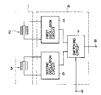
~- Referring to Fig. 1, a first surface acoustic wave (SAW)
resonator 2 and a second surface acou~tic wave resonator 3
which consist of a large number of electrode elements are
formed on a piezoelectric substrate 1. The surface acoustic
wave resonators 2 and 3 are respectively connected to first
and second oscillator circuits 5 and 6 formed on a
semioonductor integrated circuit (IC) substrate 4.
Outputs from the oscillator circuits 5 and 6 are input to
a switching circuit 7 formed on the same integrated circuit
substrate 4 as that of the oscillator circuits 5 and 6. An
output signal from the switching circuit 7 is output from an
output terminal 8. An input modulating signal is input from
an input terminal 9 to the switching circuit 7. Note that
voltages from a power source terminal (not shown) are supplied
to the circuits 5, 6, and 7 formed on the semiconductor
'
~` .
' ' ' ' `
1303679
integrated circuit substr~te 4.
In this circuit arrangement, the resonant frequencies of
the first and second surface acoustic wave resonators 2 and 3
are so set as to coincide with an output signal frequency fO
required when a digital modulating signal input from the input
terminal 9 is set at logical ~o n and an output signal
frequency fl required when the digital modulation signal input
from the input terminal is set at logical n 1 n I respectively.
The resonant frequencies of the surface acoustic wave
resonators 2 and 3 may be ~lightly offset from the actual
oscillation frequencies according to the characteristics of
the oscillator circuits S and 6. In view of this, the
resonant frequencies of the surface acoustic wave resonators 2
and 3 are sometimes determined in consideration of this
offset.
When the digital modulating signal input from the input
terminal 9 is set at logical ~0~, the switching circuit 7
~elect~ and outputs an oscillation output from the oscillator
circuit 5. However, when the digital modulating signal is set
at logical ~1~, the switching circuit 7 outputs the
oscillation output from the oscillator circuit 6.
In the clrcuit having the arrangement of Fig. 1, the
fir~t oscillator circuit 5 is oscillated at the frequency fO
corresponding to the resonant frequency of the first surface
acoustic wave resonator 2. The second oscillator circuit 6 is
oscillated at the frequency fl corresponding to the resonant
frequency of the second surface acoustic wave resonator 3.
When the digital modulating signal input from the input
~303679
the input terminal 9 i9 ~et at logical ~0l~, the signal having
the o~cillation frequency fO from the first oscillator circuit
5 is output from the output terminal 8 by the switching
circuit 7. Nhen the input digital modulating signal is set at
logical ~ , the signal having the oscillation frequency fl
from the second oscillator circuit 6 is output from the output
terminal 8. That is, an FSK-modulated signal by the digital
modulating signal input from the input terminal 9 is output
from the output terminal 8.
Note that the first and second oscillator circuits 5 and
6 are arranged by identical circuits because output levels and
temperature characteristics of these circuits are set to be
equal to each other.
Fig. 2 shows a detailed circuit arrangement showing an
arrangement of the first and second oscillator circuits 5 and
6.
The first and second oscillator circuits 5 and 6 are
formed on a single semiconductor integrated circuit substrate.
In order to minimize the interference between the oscillator
circuits, the oscillator circuits of Fig. 2 constitute a
differential amplifier circuit. Referring to Fig. 2,
transistors 100 and 101 constitute a differential
amplification transi~tor pair. The collectors of the
transistors 100 and 101 are connected to a power source
terminal 104 through resistors 102 and 103 having the same
rQsi3tance, respectively. The emitters of the transistors 100
, ~ :
and 101 are connected to a ground terminal 106 through a
common DC current source 105. The bases of the transistors
, ,
.,
,,
130~1679
100 and 101 are connected to the output termlnal of a bias
circuit 109 through resistors 107 and 108 having the same
resistance, respectively. Note that the bias circuit 109 is
connected between the power source terminal 104 and the ground
terminal 106 to generate a bias voltage.
The above circuit elements constitute the differential
amplifier circuit. The bases of the transistors 100 and 101
(the inputs of the differential amplifier circuit) are
respectively connected to connecting terminals 110 and 111 for
the surface acoustic wave resonators. The collectors of the
transistors 100 and 101 (i.e., the output of the differential
amplifier circuit) are connected to connecting terminals 112
and 113 for the surface acoustic wave resonators and output
terminals 114 and 115 of the oscillator circuits,
respectively.
The circuit having the above arrangement serves as the
oscillator circuit when the surface acoustic wave resonators 2
and 3 are connected to the connecting terminals 110, 111, 112,
and 113.
When one-port surface acoustic wave resonators 2 and 3 as
shown in Fig. 1 are connected, they are connected between one
of the connecting terminals 110 and 111 and one of the
connecting terminals 112 and 113.
In order to oscillate the above differential amplifier
circuit at a low frequency enough to serve as an ideal
amplifier which is almost free from a phase delay, the surface
acoustic wave resonators are connected between the connecting
terminals 110 and 113 or between the connecting terminal 111
~303679
and 112. In order to oscillate the differential amplifier
circuit of a high frequency, it is easy to oscillate it when
the one-port surface acoustic wave resonators are connected
between the connecting terminals 110 and 112 or between the
connecting terminals 111 and 113 because the phases of output
voltages appearing at the collectors of the transistors 100
and 101 are delayed by a time constant determined by the
resistors 102 and 103, a parasitic capacitance in the
collector-base paths of the transistors 100 and 101, and a
parasitic capacitance of the surface acoustic wave resonators.
For the sake of descriptive convenience, assume that a
one-port surface acoustic wave resonator is connected between
the connecting terminals 110 and 112 in the following
description.
An oscillation output from this oscillator circuit is
extracted as a difference between outputs from the output
terminals 114 and 115 respectively connected to the collectors
of the transistors 100 and 101.
A ratio of a power input from the one-port surface
acoustic wave resonator to the connecting terminal 110 to a
power appearing at the connecting terminal 112, that is, a
power gain of the differential amplifier is set to
sufficiently compensate for a loss of the one-port surface
acoustic wave resonator. The power gain is determined by
characteristics of the transistors 100 and 101, a current
value of the DC current source 105, and resistances of the
resistors 102 and 103.
In the circuit (Fig. 2) having the above arrangement, a
~ 303679
11
positive feedback ~ignal i~ lnput from the connecting terminal
112, i.e., the output of the different~al amplifier circuit,
to the connecting terminal 110, i.e., the input of the
differential amplifier through the one-port surface acoustic
wave resonator. The circuit of Fig. 2 i~ then oscillated, and
an oscillation output appears between the output terminals 114
and 115.
At this time, the oscillation frequency is a frequency
which lowers the impedance of the one-port surface acoustic
wave resonator, i.e., the resonant frequency. Strictly
speaking, a frequency is given such that a sum of an amount of
phase shift transmitted from one end to the other end of the
one-port surface acoustic wave resonator and an amount of
phase shift of a voltage transmitted from the connecting
terminal 110 to the connecting terminal 112 and amplified is
an integer multiple of 0 or 360.
The amount of phase shift in voltage from one end to the
other end of the one-port surface acoustic wave resonator is
abruptly changed to be about 180 within a narrow frequency
range having the resonant frequency as its center frequency.
~herefore, the circuit is oscillated at a frequency which
satisfies the above condition of the sum of the amounts of
phase shift within the narrow frequency range having the
resonant frequency as the center frequency. When the
frequency is deviated form the resonant frequency, the
impedance of the one-port surface acoustic wave resonator is
increased to increase the loss. Therefore, the differential
amplifier circuit must have an extra gain corresponding to the
~:
~3~3~79
loss of the one-port sur~ace acoustic wave resonator.
In the above description, a one-port surface acoustic
wave resonator is connected to the oscillator circuit shown in
Fig. 2. However, a two-port surface acou4tic wave resonator
may be connected to this oscillator circuit. When a one-port
surface acoustic wave resonator is connected, the differential
amplifier circuit has only one input and one output, so the
amplifier circuit cannot perform perfect differential
operation. However, when a two-port surface acoustic wave
resonator is connected to the oscillator circuit, the perfect
differential operation can be performed.
A case wherein a two-port surface acoustic wave resonator
is connected to the oscillator circuit shown in Fig. 2 will be
described.
One port of the two-port surface acoustic wave resonator
is connected to the connecting terminals 110 and 111, and the
other port of the resonator is connected between the
connecting terminals 112 and 113.
An AC voltage applied across the connecting terminals 110
and 111 of the differential amplifier circuit is amplified and
appears across the connecting terminals 112 and 113. The
phase of the output signal is inverted. The two-port surface
acoustic wave resonator is connected to have polarities such
that the voltages appearing at the two ports have inverted
phases during resonance. ~owever, when a operate at high-
frequency, phases of output voltages appearing between the
collectors of the transistors 100 and 101 are greatly delayed
by the time constant determined by the resistors 102 and 103,
~303679
a parasitic capacitance in the collector-base paths of the
transistors 100 an~ 101, and a parasitic capacitance between
the electrodes of the two-port surface acoustic wave
resonator. In this case, the oscillation can be facilitated
when voltages appearing at the two ports have the same phase
during resonance. In order to set the voltages appearing at
one port and the other port to have the same phase or opposite
phases, the connecting polarity of one of the portQ is
inverted. In some cases, the design of the two-port surface
acoustic wave resonator may be modified to shift acoustic
distances of the two port by 1/2 the wavelength.
The oscillation output of this circuit is extracted as a
difference between outputs from the output terminals 114 and
115 respectively connected to the collectors of the
transistors 100 and 101.
The power gain between the input and output terminals of
the differential amplifier circuit constituted by elements
i other than the two-port surface acoustic wave resonator, i.e,
a ratio of the power output across the connecting
terminals 112 and 113 to the power input across the connecting
terminals 110 and 111, i8 set to sufficiently compensate for
the loss of the two-port surface acoustic wave resonator. The
ratio is determined by characteristics of the transistors 100
and 101, a current value of the DC current source 105, and
resistances of the resistors 102 and 103.
In the circuit (Fig. 2) having the above arrangement, an
output from the differential amplifier circuit, i.e., an
output appearing across the connecting terminals 112 and 113,
., .
. i, ...... .
~ 3143679
is positively fed back to the input of the differential
amplifier circuit i.e., the connecting terminals 110 and lll
through the two-port surface acoustic wave resonator.
Therefore, the oscillation output appears acro~s the output
terminals 114 and 115.
In this case, the oscillation frequency is a frequency
obtained when the impedance between the ports of the two-port
surface acoustic wave resonator is lowered. Strictly
speaking, the frequency is given such that a sum of an amount
of phase shift in voltage transmitted from one port to the
other port of the two-port surface acoustic wave resonator and
an amount of phase shift in voltage transmitted from the
connecting terminals llO and 111 to the connecting terminals
112 and 113 and amplified is an integer multiple of 0 or
360.
The amount of phase shift in voltage from one port to the
other port of the two-port surface acoustic wave resonator is
abruptly changed to be about 180 within a narrow frequency
range having the resonant frequency as its center frequeney.
Therefore, the circuit is oscillated at a frequency which
satisfies the above condition of the sum of the amounts of
phase shift within the narrow frequency range having the
resonant frequency as the center frequency. When the
frequency is deviated form the resonant freguency, the
impedance of the two-port surface acoustic wave resonator is
increased to increase the loss. Therefore, the differential
amplifier circuit must have an extra gain corresponding to the
loss of the two-port surface acoustic wave resonator.
,:~
,
13~)3~i79
An effect obtained by using the oscillator circuit shown
in Fig. 2 is used in the modulator shown in Fig. 1 will be
described below. A power source current flowing form the
power source terminal 104 in the circuit of Fig. 2 consists of
a current flowing in the bias circuit 109 and a current
flowing in the DC current source lOS through the resistors 102
and 103 and the transistors 100 and 101. Therefore, the
current flowing from the power source terminal 104 consist of
only a DC component, and a high-frequency current having the
oscillation frequency does not flow from the power source
terminal 104 due to the following reason. The bias circuit
109 applies only a DC bias voltage to the transistors 100 and
101, so that only the DC current flows and a predetermined DC
current flows in the DC current source 105. The transistors
100 and 101 perform a differential operation wherein the
current of one transistor increases when the current of the
other transistor decreases. A sum of currents flowing through
the resistors 102 and 103 is always kept constant. Even if
another oscillator circuit is connected to the DC power
source connected between the power source terminal 104 and the
ground terminal 106, the oscillator circuits do not become
noise sources to each other.
Fig.3 is a detailed circuit diagram showing an
arrangement of the switching circuit 7 in Fig. 1.
Since the integrated circuit is used, the switching
circuit 7 has a differential input/output arrangement. Ona of
first differential input terminals 201 for receiving an output
from the first oscillator circuit 5 is connected to the base
,:
i,
, . ..
1303679
16
of a transistor 202, and ~he other of the first differential
input terminals 201 is connected to the base of a transi~tor
203. One of second differential input terminals 204 for
receiving an output signal from the second oscillator circuit
6 is connected to the base of a transistor 205, and the other
of the second differential input terminals 204 is connected to
the base of a transistor 206.
The emitters of the transistors 202 and 203 are connected
to the collector of a transistor 207. The emitters of the
transistors 205 and 206 are connected to the collector of a
transistor 208.
The collectors of the transistors 202 and 205 are
connected to a power source terminal 211 through a re~istor
209. The collectors of the transistors 203 and 206 are
connected to the power source terminal 211 through a resistor
210. The emitters of the transistors 207 and 208 are
connected to a ground terminal 213 through a DC current source
212. A bias circuit 214 is connected to the base of the
transistor 207. The base of the transistor 208 is connected
to a modulation input terminal 216 through a resistor 215.
The collectors of the transistors 202j 203, 205, and 206 are
connected to the differential output terminals 217. Note that
a DC power source is connected between the ground terminal 213
and the power source terminal 211.
In the circuit (Fig.3) with the above arrangement, when
the digital modulation signal input from the modulation input
terminal 216 is set at logical "0", i.e., when the potential
at the modulation input terminal 216 is sufficiently lower
)3
17
than a voltage appliad from the bias circult 214 to the ba~e
of the transistor 207, the transistor 208 is disabled to bloc~
the current. The current from the D~ current source 212 flows
through the transistor 207. In addition, the current from the
DC current source 212 flows through the resistors 209 and 210
and the transistors 202 and 203. For this reason, a signal
input terminal 201 is differentially amplified by the
transistors 202 and 203 and appears at an output terminal 217.
However, since a current does not flow in the transistor 20a,
the current does not flow in the transistors 205 and 206,
either. The transistors 205 and 206 do not serve as amplifier
elements, and the ~ignal input to the differential input
terminal 204 isn't amplified. Therefore, the signal input
from the differential input terminal 201, i.e., only the
output signal from the first oscillator ~ircuit 5 is
amplified. The amplified signal appears at the differential
output terminal 217.
When the digital modulation signal is set at logical "1",
i.e., when the potential at the modulation input terminal 216
is sufficiently higher than the voltage applied from the bias
circuit 214 to the base of the transistor 207, the transistor
207 i8 disabled, and a current does flow therethrough. The
current from the DC current source 212 flows through the
transistors 208. In addition, the current flows from the DC
current source 212 flows through the resistors 209 and 210 and
the transistors 205 and 206. Therefore, the signal input from
the differential input terminal 204 is differentially
amplified by the transistors 205 and 206, and the amplified
,,
1303679
18
ignal appears at the differential output terminal 217.
However, since a current does flow in the transistor 207,
currents do not flow in the transistors 202 and 203, either.
The transistors 202 and 203 do not serve as amplifier
elements, and the signal input from the dif~erential input
terminal 201 is not amplified. Therefore, the signal input
from the differential input terminal 204, i.e., only the
output signal from the second oscillator circuit 6 is
amplified. The amplified signal is output from the
differential output terminal 217.
As described above, in the switching circuit shown in
Fig. 3, when the digital modulating signal is set at logical
"0-, the signal input from the differential input terminal 201
i8 amplified, and the amplified signal is output. However,
when the digital modulating signal is set at logical n 1~ ~ the
signal input from the differential input terminal 204 is
amplified, and the amplified signal is output. Since a
capacitor and a resistor having a high resistance which
increase a time constant are not included in the switching
circuit, the circuit can be operated at high speed.
The transistors 202 and 203, and the transistors 205 and
206 in Fig. 3 serve as differential amplifiers, respectively.
Even if noise is applied between the ground terminal 213 and
the power source terminal 211, or between the input terminals
201 and 204, the input noise can be eliminated and is not
output from the differential output terminal 217. A current
flowing from the power source connected between the ground
terminal 213 and the power source terminal 212 to the
`~ 1303~79
19
switching circuit consi~t~ of only a current flowing in the
bias current 214 and a current flowing through the DC current
source 212. Therefore, only the DC current flows in the
switching circuit. The switching circuit shown in Fig. 3 does
not become a noise source for other circuits (e.g., an
oscillator circuit) connected to the power source.
The switching circuit shown in Fig. 3 is suitable for an
integrated circuit due to the above reasons.
The effect of the embodiment shown in Fig. 1 will be
described below. The switching circuit 7 shown in Fig. 1
simply selects one of the outputs from the oscillator circuits
S and 6 and outputs the selected signal. For this reason, the
switching circuit can be operated at high speed and can easily
cope with a change in digital modulating signal input from the
input terminal 9. Therefore, even if the bit rate of the
digital modulating signal is high, no problem is posed.
The frequency fO of the output signal obtained when the
digital modulating signal is at logical ~'O" and the frequency
fl of the output signal obtained when the digital modulating
signal is at logical "1" can be independently determined by
the surface acoustic wave resonators 2 and 3, respectively.
For this reason, the frequencies fO and fl can be set
independently of the loaded Qs of the surface acoustic wave
resonators 2 and 3. Resonators having large loaded Qs and
excellent temperature characteristics can be used as the
surface acoustic wave resonators 2 and 3. Therefore, a stable
FSK signal source having low phase noise can be obtained.
Furthermore, since the surface acoustic wave resonators 2
''
' :
,, .
1~0~
and 3 are orm~d on the in~le piezoelectric sub~trate
l, variations in resonant frequencies of the resonators during
mass production equally occur in both the resonators 2 and 3.
More specifically, when the resonant frequency of one
resonator is decreased, the resonant frequency of the other
resonator is decreased accordingly, and vice versa.
Similarly,-since the oscillator circuits 5 and 6 are formed on
the single semiconductor substrate 4, characteristic
variations between them are small. Therefore, the difference
between the frequencies fO and fl can be maintained constant
without adjustment even during mass production.
The embodiment shown in Fig. 1 can be realized by two
chips, i.e., a chip of the piezoelectric substrate l, and a
chip of the semiconductor integrated circuit substrate 4.
The package of the resultant circuit arrangement can be made
compact.
The present invention is not limited to the particular
embodiment described above. Various changes and modifications
may be made within the spirit and scope of the invention.
Fig. 4 is a diagram showing a circuit according to
another embodiment of the present invention. The same
reference numerals as in the first embodiment denote the same
parts in the second embodiment, and a detailed description
thereof will be omitted.
First, second,third, and fourth surface acoustic wave
resonators 2, 3, 10, and 11 are formed on a piezoelectric
substrate 1, and are connected to first, second, third, and
fourth oscillator circuits 5, 6, 12, and 13 formed on a
~30;~679
semiconductor integrated circuit substrate 4, respectively.
Output signals from the oscillator circuits 5, 6, 12, and 13
are input to a switching circuit 14 for~ed on the integrated
circuit substrate 4. An output signal from the switching
circuit 14 appears at an output terminal 8. A 2-bit
modulation input signal is input from input terminals 15 and
16 to the switching circuit 14. Note that a voltage is
applied from a power source terminal (not shown) to each of
the above circuits.
In the circuit (Fig. 4) having the above arrangement,
when a two-bit digital modulating signal input from the input
terminals 15 and 16 is set to be ~00~, a signal having an
oscillation frequency fO from the first oscillator circuit 5
appears at the output terminal 8. However, when the two-bit
digital modulating signal is set to be n 011l 1 a signal having
an oscillation frequency fl from the second oscillator circuit
6 appears at the output terminal 8. When the two-bit digital
modulating signal is set to be "10", a signal having an
oscillation frequency f2 from the third oscillator circuit 12
appears at the output terminal 8. When the two bit digital
modulating signal is set to be "11", a signal having an
oscillation frequency f3 from the fourth oscillator circuit 13
appears at the output terminal 8. That is, four-value FSK
modulation by using the two-bit digital modulating signal
input from the input terminals 15 and 16 can be performed.
Other circuit operations of the second embodiment are the same
as those of the first embodiment shown in Fig. 1.
Substantially the same effect as in the first embodiment
.,
,
1303679
can be obtained in the second embodiment.
Similarly, FSX modulation of three values or five or more
values may be achieved.
According to the present invention, a high-performance
FSK modulator as described above can be arranged. A
transmitter using FSK modulation according to still another
embodiment of the present invention can be arranged.
Fig. 5 is a diagram showing an FSX modulator serving as a
transmitter.
Referring to Fig. 5, first and second two-port surface
acoustic wave resonators 21 and 22 are formed on a
piezoelectric substrate 1 and are connected to first and
second oscillator circuits 23 and 24 formed on a semiconductor
integrated circuit substrate 4, respectively.
Outputs from the oscillator circuits 23 and 24 are input
to a switchin~ circuit 25 formed on the same semiconductor
integrated circuit substrate 4 as that of the oscillator
circuits 23 and 24. An output signal from the switching
circuit 25 is amplified by a power amplifier circuit 26, and
the amplified signal is output to an output terminal 8. A
modulation input signal is input from an input terminal 9 to
the switching circuit 25.
The oscillator circuits 23 and 24, the switching circuit
25, and the power amplifier circuit 26 have a function for
simultaneously varying power consumption and an output signal
level. Output xignals from a power control circuit 27 formed
on the semiconductor integrated circuit substrate 4 are
respectively input to the control terminals, i.e., power
1303679
23
control terminals of these circuits. The power control
circuit 27 has two inputs: one input is used to set current
consumption and the output levels of all circuit~ formed on
the semiconductor integrated circuit substrate 4 and is
connected to an input terminal 28; and the other input i8 used
to enable or disable all the circuits formed on the
semiconductor integrated circuit substrate 4 and is connected
to an input terminal 29. Note that a voltage is applied from
a power source terminal (not shown) to the circuits 23, 24,
25, 26, and 27 formed on the semiconductor integrated circuit
substrate 4.
For the sake of descriptive convenience, assume that a
signal for operating all the circuits, e.g., a digital signal
of logical "1" is input to the input terminal 29, a power
setting resistor is connected between the input terminal 28
and a power source (not shown), and all the circuits are
operated with predetermined current consumption. Also assume
that an antenna is connected to the output terminal 8 through
a matching circuit (not shown).
The antenna may be directly connected to the output
term~nal 8 through the matching circuit.
The piezoelectric substrate 1 and the semiconductor
integrated circuit substrate 4 of F~g. 5 are mounted in a
single package.
A resonant frequency of the first two-port surface
acoustic wave resonator 21 and a resonant frequency of the
second two-port surface acoustic wave resonator 22 are so set
as to coincide with an output signal frequency fO required
~'
1303679
24
when the digital modulating ~ignal Lnput ~rom the input
terminal 9 is at logical ~0~ and an output signal ~requency fl
required when the digital modulating signal is at logical "1",
respectively. The resonant frequencie~ of the surface
acoustic wave resonators 21 and 22 may be slightly deviated
from the actual oscillation frequencies due to the
characteristics of the oscillator circuits 23 and 24. The
resonant frequencies of the surface acoustic wave resonators
21 and 22 are designed in consideration of the above deviation
in some cases.
When the digital modulating signal input from the input
terminal 9 is set at logical ~0~, the switching circuit 25
selects an oscillation output from the oscillator circuit 23.
However, when the signal is set at logical ~ , the switching
circuit 25 selects an oscillation output from the oscillator
circuit 24.
In the circuit (Fig. 5) having the above arrangement, the
first oscillator circuit 23 is oscillated at the frequency fO
corresponding to the resonant frequency of the first
two-port surface acoustic wave resonator 21. The second
oscillator circuit 24 is oscillated at the frequency fl
corresponding to the resonant frequency of the second two-port
surface acoustic wave resonator 22. When the digital
modulating signal input from the input terminal 9 to the
switching circuit 25 is set at logical ~'0~', the signal of the
oscillation frequency fO from the first oscillator circuit 23
is output. However, when the digital modulating signal is set
at logical "1", the signal of the oscillation frequency fl
i303679
from the second osclllator circult 24 i8 output. That i8, an
FSK-modulated signal by the digital modulating signal input
from the input terminal 9 is output from the switching circuit
25.
The FSX-modulated signal is amplified by the power
amplifier circuit 26 and radiated as a radio wave from an
antenna connected to the output terminal 8 through the
matching circuit.
The first and second oscillator circuits 23 and 24 can be
constituted by identical circuits in the same manner as in the
first embodiment.
Fig. 6 is a circuit diagram showing an arrangement of the
first and second oscillator circuits 23 and 24.
The oscillator circuit shown in Fig. 6 is a modification
of the oscillator circuit of Fig. 2 and is constituted by a
differential amplifier arrangement in the same manner as in
Fig. 2.
Referring to Fig. 6, transistors 100 and 101 constitute a
differential amplification transistor pair. The collectors of
the transistors 100 and 101 are connected to a power source
terminal 104 through the collector-emitter paths of
transistors 116 and 117 and resistors 102 and 103 having the
same resistance. The emitters of the transistors 100 and 101
are connected to a ground terminal 106 through a common DC
current source 118. The ~ases of the transistors 100 and 101
are connected to one output of a bias circuit 119 through
resistors 107 and 108 having the same resistance.
The ba~es of transistors 116 and 117 are directly
~303679
26
connected to the other output of the bias clrcuit 119. The
bases of transistors 120 and 121, the collectors of which are
connected to the power source terminal 104, are connected to
the collectors of the transistors 116 and 117, reRpectively.
The emitters of the transistors 120 and 1~1 are connected
to the ground terminal 106 through the collector-emitter paths
of transistors 122 and 123 and DC current sources 124 and 125.
The bases of the transistors 122 and 123 are connected to the
collectors thereof, so that the transistors 122 and 123 serve ,
as diodes. The DC current sources 118, 124, and 125 have a
function for varying their current values, and their control
terminals are connected to the power control terminal 126.
The bias circuit 119 is connected to the power source terminal
104 and the ground terminal 106 to constitute a power source
and has a function for varying current consumption. The
control terminal of the bias circuit 119 is connected to the
power control terminal 126.
The above circuits constitute a differential amplifier
circuit. The bases of the transistors 100 and 101 (i.e., the
input of the differential amplifier circuit) are connected to
connecting terminals 110 and 111 for the surface acoustic wave
resonators. The emitters of the transistors 122 and 123
(i.e., the output of the differential amplifier circuit) are
connected to connecting terminals 112 and 113 for the surface
acou~tic wave resonators, respectively. Outputs from the
oscillator circuits are obtained from output terminals 114 and
115 respectively connected to the bases of the transistors 100
and 101.
.',
,.
.,
~.3036'79
For the sake of descriptive convenience, a~sume that a
control signal from the power control circuit 27 of Fig. 5 is
applied to the power control terminal 126, current consumption
of the DC current sources 118/ 124, and 125 is regulated to be
a predetermined value, and the DC current sources are operated
under this condition.
The circuit (Fig.6) having the arrangement described
above can be operated as an oscillator circuit when one- or
two-port surface acoustic wave resonators are connected to the
connecting terminals 110, 111, 112, and 113. A method of
connecting the surface acoustic wave resonators and their
operation are the same as those in Fig. 2, and a detailed
description thereof will be omitted. Only differences will be
described below.
The collector potentials of the transistors 100 and 101
serving as the differential amplification pair are set at
values obtained by subtracting base-emitter voltages (i.e.,
about 0.7 V) of the transistors 116 and 117 from the voltages
applied from the bias circuit 119 to the bases of the
transistors 116 and 117. Therefore, the collector potentials
of the transistors 100 and 101 are kept substantially constant
even in the oscillation state. In particular, the collector
AC voltage which poses a problem in the case of a high-
frequency arrangement is negatively fed back by the parasitic
capacitance of the collector-base paths of the transistors 100
and 101. But as the collector potentials of the transistors
100 and 101 are kept substantially constant even in the
oscillation state, the gains of the transistors 100 and 101
1303679
28
are thus equivalently reduc~d.
Colle~tor currents of the transistors 100 and 101 flow
through the resistors 102 and 103 and the collector-emitter
paths of the transistors 116 and 117. AC signals input from
the connecting terminals 110 and 111 are amplified, and the
amplified signals are input to the bases of the tran~istors
120 and 121.
- A circuit consisting of the transistors 120 and 122 and
the DC current source 124 and a circuit consisting of the
transistors 121 and 123 and the DC current source 125 serve as
so-called emitter follower buffer amplifiers, respectively.
The AC voltages applied to the bases of the transistors 120
and 121 are output form the connecting terminals 112 and 113
through the emitter follower buffer amplifiers, respectively.
Since the signals are output through the buffer amplifiers,
the circuit of Fig. 6 is not adversely affected by the
impedances of the surface acoustic wave resonators, thereby
obtaining a stable signal. An output from the oscillator
circuit is obtained by the base of each of the transistors 100
and 101. However, this output may be obtained from the
collector of each of the transistors 116 and 117 or the
emitter of each of the transistors 122 and 123.
In the oscillator circuit of Fig. 6, a current flowing
from the power source connected between the power source
terminal 104 and the ground terminal 106 entirely flows
through the DC current sources 118, 124, and 125, and the bias
circuit 119. The current values of the DC current sources
118, 124, and 125 and the current consumption of the bias
1303679
29
circuit 119 can be ad~usted by a signal applied to the power
control terminal 126. That is, the current consumption of the
entire circuit can be controlled by the signal applied to the
power control terminal 126. In some cases, the current
consumption of the entire circuit can be set to be zero to
stop the circuit operation, i.e., the circuit can be set in
the standby state. When the current values of the DC current
- -- sources 118, 124, and 125 are changed, values of currents
flowing through the transistors are changed accordingly, so
that the gain of the differential amplifier circuit is also
changed. Therefore, the level of the oscillation output from
the output terminals 114 and 115 can also be controlled by the
signal applied to the power control terminal 126 in addition
to the current consumption of the entire circuit.
An effect obtained by using the oscillator circuit of
Fig. 6 as the transmitter of Fig. 5 will be described below.
Referring to Fig. 6, a current flowing from the power source
connected between the power source terminal 104 and the ground
terminal 106 to the circuit of Fig. 6 entirely flows through
the DC current sources 118, 124, and 125 and the bias circuit
119. Therefore, the current flowing from the power source
consists of only a DC current and does not include a high-
frequency current. For this reason, even if another
o~cillator circuit is connected to the power source, the
oscillator circuits do not serve as noise sources to each
other.
As another effect, the current consumption of the entire
circuit and the oscillation output level c~n be controlled.
;:
1303~7g
In the above description, the oscillator circuits of Fig.
6 are exempli~ied as the first and second oscillator circuits
of Fig. 5.
Fig. 7 is a detailed circuit diagram showing an
arrangement of the switching circuit 25 shown in Fig. 5.
Since an integrated circuit is used, the ~witching
circuit 25`has a differential input/output arrangement.
One of first differential input terminals 201 for
receiving output signal from the first oscillator circuit 23
is connected to the base of a transistor 218, and the other of
the first differential input terminals 201 is connected to the
base of a transistor 219. One of second differential input
terminals 204 for receiving the output signal from the second
oscillator circuit 24 is connected to the base of a transistor
220, and the other of the second input terminals 204 is
connected to the base of a transistor 221.
The emitters of the transistors 218 and 219 are conn~cted
to a ground terminal 213 through a first common DC current
source 222. The emitters of the transistors 220 and 221 are
connected to the gxound terminal 213 through a second common
DC current source 223.
The emitters of transistors 224 and 225 are connected to
the collector of the transistor 218, and the emitters of
transistors 226 and 227 are connected to the collector of the
transistor 219. The emitters of transistors 228 and 229 are
connected to the collector of the transistor 220. The
emitters of transistors 230 and 231 are connected to the
collector of the transistor 221. The bases of the transistors
13036'79
31
224, 227, 228, and 230 are connected to a first modulation
input terminal 232. The bases of the transistors 225, 226,
228, and 231 are connected to a second modulation input
terminal 233. The collertors of the transistors 224 and 228
are connected to a power source terminal 211 through a
resistor 234. The collectors of the transistors 227 and 231
are connected to the power source terminal 211 through a
resistor 235. The collectors of the transistors 225, 226,
229, and 230 are directly connected to the power source
terminal 211.
The collectors of the transistors 224 and 228 are
connected to one of differential output terminals 217, and the
collectors of the transistors 227 and 231 are connected to the
other of the differential output terminals 217.
The first and second DC current sources 222 and 223 have
a function for varying a current value. The control terminals
of the current sources 222 and 223 are connected to a power
control terminal 236. For the sake of descriptive
convenience, assume that a control signal from the power
control circuit 27 of Fig. 5 is applied to the power control
terminal 236, current values of the DC current sources 222 and
223 are controlled to be predetermined values, and the current
sources 222 and 223 are operated under this condition.
Inputs from the first and second modulation input
terminals 232 and 233 serve as differential inputs. In the
following description, assume that the digital modulation
signal is converted into a differential signal which is then
applled to tho modulation input terminals 232 and 233, and
~,
i303679
32
that a potential at the fir~t modulation input t~rminal 232 i8
sufficiently hiqher than that at the second modulation lnput
terminal 233 when the diqital modulation signal is at logical
~0~, and a potential of the second modulation input terminsl
233 is sufficiently higher than that at the first modulation
input terminal 232 when the digital modulation signal i8 at
logical ~
In the switching circuit (Fig. 7)-having the above
arrangement, when the digital modulating signal is set at
logical "0", i.e., when the potential at the first modulation
input terminal 232 is sufficiently higher than that at the
second modulation input terminal 233, base potentials at the
transistors 225, 226, 228, and 231 are lower than base
potentials at the transistors 224, 227, 229, and 230. The
transistors 225, 226, 228, and 231 are turned off, and
currents do not flow therethrough. For this reason, collector
currents of the transistors 218 and 219 flow through the
resistors 234 and 235 and the collector-emitter paths of the
transistors 224 and 227. Collector currents of the
transistors 220 and 221 flow through the collector-emitter
paths of the transistors 229 and 230. Therefore, the signal
input from the differential input terminals 201 is
differentially amplified by the transistors 218 and 219, and
the differentially amplified signal is output across the
output terminals 217. However, since the collector currents
of the transistors 220 and 221 do not flow through the
resistors 234 and 235, the signal input from the differential
Lnput terminals 204 are not output from the output termLn~ls
1303~79
217. That is, only tha output signal input from the
oscillator circuit 23 to the differential input terminals 201
is amplified and appear across the output terminals 217.
When the digital modulating signal is set at logical H 11l r
i.e., when a potential at the second modulation input terminal
233 is sufficiently higher than at of the first modulation
input terminal 232, base potentials of the transistors 224,
227, 229, and 230 are lower than those of the transistors 225,
226, 228, and 231. The transistors 224, 227, 229, and 230 are
turned off, and currents do not flow therethrough. For this
reason, the collector currents of the transistors 220 and 221
flow through the resistors 234 and 235 and the collector-
emitter paths of the transistors 228 and 231. ~he collector
currents of the transistors 218 and 219 flow through the
collector-emitter paths of the transistors 225 and 226. The
signal input across the differential input terminals 204 is
differentially amplified by the transistors 220 and 221, and
the differentially amplified signal is output across the
output terminals 217. However, since the collector current~
of the transistors 218 and 219 do not flow through the
resistors 234 and 235, the signal input from the differential
input terminals 201 is not output across the output terminals
217. That is, only the output signal from the oscillator
circuit 24 to the differential input terminals 204 is
amplified, and the amplified signal is output across the
output terminals 217.
As described above, in the switching circuit shown in
Fig. 7, when the digital modulating signal is set at logical
:
~303679
34
0~, the signal input acro~s the differential input terminals
201 is ampli~ied and output. However, when the digital
modulating signal is set at logical ~1", the signal input from
the differential input terminals 204 is amplified and output.
Since a capacitor and a resistor having a high resistance
which increase a time constant are not present in the
switching circuit, the switching circuit can be operated at
high speed.
Referring to Fig. 7, the transistors 218 and 219 and the
transistors 220 and 221 serve as differential amplifiers,
respectively. Even if noise is applied bstween the ground
terminal 213 and the power source terminal 211 or between the
input terminals 201 and 204, noise can be eliminated and is
not output across the differential output terminals 217. In
addition, a current flowing from the power source connected
between the ground terminal 213 and the power source terminal
211 to the switching circuit consists of a current flowing
through the first DC current source 222 and current flowing
through the second DC current source 223. That is, the
current consists of only the DC current. For this reason, the
switching circuit shown in Fig. 7 does not become a noise
source for other circuits (e.g., an oscillator circuit)
connected to the power source.
In the switching circuit as described above with
reference to Fig. 7, all currents flowing from the power
source connected between the power source terminal 211 and the
ground terminal 213 flow through the DC current sources 222
and 223. The current values of the DC current sources 222 and
130~679
223 can be controlled by the signal applied to the power
control terminal 236. That ls, the current consumption of the
entire switching circuit can be controlled by the signal
applied to the power control terminal 236. In some cases, the
current consumption of the entire circuit can be set to be
zero to stop the circuit operation, i.e., the circuit may be
set in the standby state. When the current values of the DC
current sources 222 and 223 are changed, values of currents
flowing through the transistors are changed accordingly, so
that the gain of the differential amplifier circuit is also
changed. Therefore, the level of the output signal from the
output terminals 217 can also be controlled in addition to the
current consumption of the entire circuit.
The switching circuit shown in Fig. 7 has a feature of a
high switching speed. For example, in the switching circuit
shown in Fig. 3, an input signal supposed not to be output may
leak to the output terminal or the opposite input terminal by
a parasitic capacitance of the collector-base paths of the
transistors 202, 203, 205, and 206. However, in the switching
circuit shown in Fig. 7, the transistors 224, 227, 228, and
231 are connected between the collectors of the transistors
218, 219, 220, and 221 and the output terminal 217 and between
the collectors of the transistors 218 and 219 and the
collectors of the transistors 220 and 221. Therefore, even if
a parasitic capacitance is pre~ent in the collector-base paths
of the transistors 218, 219, 220, and 221, the leakage signal
has a very small magnitude, and the switching speed can be
increased.
1303679
36
An arrangement o the switching clrcult 25 of Flg. 5 i8
exempli~ied in Fig. 7.
The transmitter shown in Fig. 5 includes the power
amplifier circuit 26 and the power control circuit 27 ~n
addition to the oscillator circuits 23 and 24 and the
switching circuit 25.
A circuit arrangement may be employed to obtain a
sufficient output power from the power amplifier circuit 26.
It is preferable to arrange the circuit so as to control the
current consumption of the entire circuit and the output
signal level. When power conversion efficiency is taken into
consideration, it is often more preferable to arrange a
single-end circuit than a differential amplifier circuit. In
this case, since the oscillator circuits and the switching
circuit have a differential amplifier circuit arrangement and
are not easily adversely affected by other circuits, the power
amplifier circuit need not have a differential amplifier
circuit arrangement. In this case, if an output from the
switching circuit is a differential output, one of the output
terminals i8 used.
The power control circuit is arranged such that a current
flowing from the power source through the power setting
resistor connected to the input terminal 28 is converted into
a control signal, and this control signal is supplied to the
respective circuits. The power control circuit is preferably
arranged to change current consumption in accordance with a
resistance of the power setting resistor. The power control
circuit iR arranged to have a function for enabling and
1~03679
37
disabling the respective circui~s connected to the output and
the power control circuit itself in accordance with a signal
input from the input terminal 29.
An effect of the embodiment shown in Fig. 5 will be
described below.
The circuit of Fig. S has the same effect as the
embodiment of Fig. 1 as far as the FSK modulation function is
concerned. In addition, almost all the functions of the
circuit (Fig. 5) as the transmitter are incorporated in a
single package. Therefore, a compact transmission system can
be arranged when a power source, an antenna, its matching
circuit, and a power setting resistor are connected to the
transmitter. The current consumption and the output signal
level can be optimally controlled by the externally connected
power setting resistor.
The circuit of Fig. 5 can be enabled or disabled by an
external circuit. The current consumption of the entire
cixcuit is set to be almost zero, and the circuit is set in a
so-called standby state.
The embodiment shown in Fig. 5 has been described.
; The oscillator circuits and the switching circuit used in
the present invention are not limited to those shown in Figs.
2, 3, 6, and 7.
For example, the DC current source 105 and the bias
circuit 109 in the oscillator circuit (Fig. 2), and the DC
current source 212 and the bias circuit 214 in the switching
, - circuit (Fig. 3) may have a current variable function and a
current consu~ptlon varlable function. ~herefore, these
,,
.,
13036'79
o~cillator circuit and switching circuit may be used in place
of the oscillator eircuit and the switching circuit shown in
Flg. 5.
In fine, any oscillator and switching circuits may be
used if functions necessary in the present invention can be
obtained.
In the embodiment of Fig. 5, the power control function,
i.e., the power control circuit 27 may be omitted. In this
ease, the power eonsumption eontrol function and the output
signal level eontrol funetion are omitted from other
eireuits. When a necessary power can be obtained from an
output from the switching circuit 25, the power amplifier
circuit 26 can be omitted.
In the above-mentioned embodiments and their
modifieations, the surfaee aeoustie wave resonators are
formed on a signal piezoelectxic substrate. However, the
present invention is not limited to this. A plurality of
sur~aee aeou~tle wave resonators may be formed on a plurality
o~ plezoeleetrle sub~trates if their materials are identieal.
In the above embodiments and their modifieations, the
surfaee aeGustie wave resonator is oseillated. However, the
oseillator ¢ireuit is not limited to this. Oseillation may
be performed by using, e.g., a 6urfaee aeou~tie wave filter,
a surfaee aeoustie wave delay line, a erystal resonator, a
eeramie resonator, or the like. In this ease, shapes of
~303679
39
electrodes formed on the plazoelectric ~ubstr~tes may be
individually designed. In this case, a plurality of
resonators may be formed on a single piezoelectric substrate
or individual piezoelectric substrates if their materials are
identical.
In addition to the oscillator circuit~ and the switching
circuits, other circuits such as an amplifier circuit for
amplifying an input/output signal and a circuit for converting
an output signal into a digital signal may be formed on the
semiconductor integrated circuit substrate.
The present invention has been described with reference
to the particular embodiments and their modification. The
present invention is not limited to these. Various changes
and modifications may be made within the spirit and scope of
the invention.
..
.