Note: Descriptions are shown in the official language in which they were submitted.
~03688
The present invention relates to a frequency-dividing
circuit in a semiconductor integrated circuit or the ~ike.
A prior art of the field concerned is shown in Denshi
Joho Tsushin Gakka1 Soritsu 70-Shunen K1nen Soao Zenkoku
Taika1 Koen RoDbu ~h~ (Papers from the 70th Anniversary
Memorial Meeting of the Institute of Electronics,
Information and Communication Engineers of Japan), No. 396
(Sho 62), Osafune, Enoki, Muraguchi and Owada "20GHzGaAs
Dynamic Frequency-Divider", pages 2-200. This prior art
will be explained with reference to the drawings.
Fig. 1 is a block diagram showing an example of a
prior-art frequency-dividing circuit;
Fig. 2 is a block diagram showing a circuit diagram of
the frequency-dividing cir_uit shown in Fig. 1;
Fig. 3 is a timing chart for explaining the operation
of the frequency-dividing circuit shown in Fig. 2;
Fig. 4 is a block diagram showing a frequency-dividing
circuit of a first embodiment of the invention;
Fig. 5 is a timing chart for explaining the operation
of the frequency-dividing circuit ~hown in Fig. 4;
Fig. 6 and Fig. 7 are block diagrams showing frequency-
dividing circuits of a second and third embodiments of the
invention;
7T~
'.'~; ~,, 1
.~ , ' . .
.
, ', -
~3036~a
Fig. 8 is a timing chart for explaining the operation
of the frequency-dividing circuit shown in Fig. 7.
Fig. 9 is a block diagram showing a frequency-dividing
circuit of a fourth embodiment of the invention; and
Fig. 10 is a block diagram showing a frequency-dividing
circuit of a fifth embodiment of the invention.
In the frequency-dividing circuit shown in Fig. l, an
inverter l, a switch 2, a source-follower circuit 3, and a
switch 4 are connected in a ring. The inputs of the
respective inverters l and 3 are connected through
capacitors 5 and 6 to the ground. An output terminal OUT is
connected to the output of the source-follower circuit 3.
Fig. 2 is a circuit diagram of the frequency-dividing
circuit in Fig. l.
In this frequency-dividing circult, the inverter l is
la
`'~
1303688
comprised of a fleld-e~`oet t:ranslsl;ol (llelelllufler.r(l~elr(~(l
to as FET) la, lb, lc and l~i an(l Scho~ky ~lio(le le an(l 11.
rrhe switches 2 and 4 are comprlse~ ol l~l~'l's ~a all(l 4a,
respectively, and the sonrce-rol.lo~Yer c:lrcu.ll .3 .Is coml)rl~qed
o-f FETs 3a and 3b. Tlle capucJ~or 5 In l;`l~ Is a
representation by a concentrate(i cons~allt ol` ~lle lnp~lt
capacitance of the ga~e of tlle I~EI'I.I) arl(l tile cal~a(:itall(c ol
the wiring conductor connected to tl~e ~ate. Silnilarly, t:llc
capacitor 6 is a representation by a concentrated constant
of the input capacitance of tlle gatc oi the iE'r3a and tlle
capacitance of the wlring con(lllctor connectc(l to the ~alc.
Vdd and Vss in ~ig. 2 arc a fi.rst all(l se(orl(l powe
supply potentials, CK is a clock Slgllal, CK .I.S an inVCl'~('(
clock signal, and N1, N2 and N3 are nodes.
The operation of the frequency-(iividing circuit will
first be described with reference to l~i.g. 1.
It is assumed that, initlally, the capacltarlce 5 i~
charged, the switch 2 is closed and tl~e swlt:(ll 4 .is ol)ell.
In this state, a Higll signal (an "Il" level slgnal) is -led to
the input of the inverter 1, and a Low signal (an "L" level
signal) is delivered from the output of t}le inverter 1.
Since the switch 2 is closed, t}le capacitallce 6 is
discharged and a Low signal is fed to the Illpllt of the
source-follower circuit 3, and the OUtpllt ol` ~he source-
follower circuit 3 is Low.
. .
.: 2
,
i....
: . .
'' . '
~303688
When the switcll 2 Is ol~e~ r~ o sw I l cl~ 4 I;s
closed, since the output Or ~lle sO~lr('C-fOL].OW(`r cl rcu.l~ :3 .I.s
Low, the capacltance 5 .Ls dlscllarge(l a~ e In~ t or ~;ll(!
inverter 1 becomes Low, and hence tlle Oll~[)Ut o:r tlle .Invelter
1 becomes Illgh.
When the switch Z is closed and tlle switcl~ 4 is operled,
the capacitance 6 is char~ed by the ou~put ol` tlle inverter
1, and a High signal appears at the Inpllt o~ t;he source-
follower circuit 3 and a lilgll sl~lla.l ~Il)l)cars ~It t~e out~ of
the source-follower circult 3.
Accordingly, a si~nal havin~ a l)criod tw:Lce that of the
opening and closing period of the swltclles 2 and 4 is fed to
the output terminal OUT connected to the out~ t Or the
source-follower circuit 3. Thus, the circuit operates as a
frequency-dividing circuit.
When the capacitance 5 is charged Wit}l the switch 4
open, the charge on the capacitance 5 is discllar~ed by a
leak current through the input impedarlce of tlle inverter 1
and the switch 4, so it is impossible for thls state to
contlnue for a more than a certain tlme. Slmllarly, the
charge on the capacitance 6 wlli:Le tlle swltch 2 is open
cannot last long because o-f a leak cl~rrerlt tllrollgl~ the .IIlput
impedance of the source-follower clrcult; ~3 a0(l tl~e swl.~cl) 2.
The frequency-dividing circuit tl~erelore oper2ltes as a
dynamic frequency-dividin~ circuit wl~lcll perl`orms the
~'
1303688
frequency-dlviding operat:lor1 on s1~nal~ of` a lerlod w1tl11l u
certain range whlch is limited i~y thc charglr1g and
dLscharging tlme o~ tlle capac3.tances ~ and ~ asld thc dc.l.ay
time from the input to tlle output ol t;lle irlv(!rter 1 an(l 1.11(!
source-~ollower circult 4.
Next the operation of the fre(i~lerl(:y-(11vidlr'g circ~
in Flg. l will be descrlbe(i in furt~lel det~1:1 wltl1 relclcncc
to the tlmlng chart of Eig. 3.
It is assumed that initlally tll( clock sigr1al CK tlle
nodes N2 and N3 and the output termlnal OUT are Low w~1i:Le
the inverted clock sigrlal CK and tl1c nodc N2 are 11igil. \VIIcr
the clock signal CK changes from Lo~v to lligll ur1(1 the
inverted clock signal CK changes from 11igtl ~o Low the
signal on the node Nl is transferred through the ~ET 2u ~o
the node N2 and the node N2 tllerefore char1ges from Low to
Hlgh. The output termlnal OUT therefore cha11ges from Low to
11igh. When the clock signal CK changes trom lligh to Low
and the lnverted clock slgnal CK chan~es frolll Low to l1
the slgnal on the output terminal OU1 is trarlsferred tl1rol1g~1
the FET 4a to the node N3 and tlle node N3 tl~erefore cl1ar1~es
~rom Low to Hlgh. The node Nl therelore charlges from 111 gh
to Low. In this way a signa.l havi11g a l)erlod twi.ce tl1at Or
the clock slgnal CK and the l~rverted <:Lock sl~nal CK ~ eurs
- at the output termina]. OU r . Il1e clrcl11t t~n1s operates us u
~- frequency-dlviding circuit.
~,. .. . . .
~ 4
~ ~'
, :
'
,~ ', .:
','~: ' ' .
i303688
The frequency-dividing circuit of the structure
described above has the following problems.
In the frequency-dividing circuit in Fig. 2, if there
is a delay between the phases of the clock signal CX and the
inverted clock signal CK, and the interval for which they
are both Low or both High is long, in which interval the
levels on the various nodes are indèfinite, and the circuit
fails to operate successfully as a frequency-dividing
circuit. That is, this circuit requires two-phase clock
signals to be input, and their phases to be adjusted
optimally.
An object of the invention is to provide a frequency-
dividing circuit which does not require two-phase clock
signals and whose operation is not greatly affected by the
phase difference of the two-phase clock signals.
A frequency~dividing circuit according to the present
invention comprises a latch circuit having first and second
complementary terminals. First and second delay circuits
each have an input and an output, each of said first and
second delay circuits comprising a series of cascading
.~
-~ i3~3688
inverters, each said delay circuit being arranged to drive
said latch circuit. First and second switche~ each have a
respective control electrode, said control electrodes being
coupled to receive an input signal, each of said switches
being turned on and off in response to the input
signal applied to its control electrode. Each said switch
couples an output from a respective one of said delay
circuits to a respective one of said complementary terminals
and to an input to a said delay circuit.
In the frequency-dividing circuit configured as
descri~ed above, the latch circuit serves to temporarily
store the states of the circuit. When the switches are
turned from off to on the outputs of the first and second
delay means are transferred through the switches to invert
the latch circuit, and the new states of complementary
terminal of the latch circuit are transferred through the
delay means and appear at the outputs of the delay means.
This means that the states of the circuit are inverted.
This inversion takes place each time the switches are turned
from off to on, while the states of the circuit do not
change when the switches are turned from on to off. The
r.
' ~
~303~;88
propagation delay time through the switches and the delay
means should be so set as to be longer than the time for
which the input signal assumes the level for turn:ing on the
switches, and shorter than the period of the input signal.
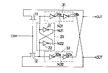
Fig. 4 is a block diagram showing a freguency-dividing
circuit of an embodiment of the invention.
This frequency-dividing circuit comprises a latch
circuit 20 having a fir~t and second complementary terminals
or nodes N21 and N22. The latch circuit 20 of this
em~odiment comprises a first and second inverters 21 and 22.
The output of the first inverter 21 forms the first
complementary terminal N21 and is connected to the input of
the second inverter 22. Similarly, the output of the second
inverter 22 forms the second complementary terminal N22 and
is connected to the input of the first inverter 21. In
other words, these inverters 21 and 22 are cross-coupled.
The frequency-dividing circuit further comprises a
first and second transistors, e.g., first and second FETs 11
and 12, turned on and off by a clock signal CK. The gates
(control electrode) of the FETs 11 and 12 are connected to
receive the clock signal CK. The source (second electrode)
i ,~
` ~
3688
of the first FET 11 i~ connected to the input of the first
inverter 21, the output of the second inverter 22 and the
input of a first inverter series 31. The source (se~ond
.
- 8
'
.. ....
i3~)3688
electrode) o-~ tl~e sec(>r)~ rl 12 Is eoo1~c(~ (1 lo ~I)e o)~ll>~l
of the first inverter 21 the Inpllt <>~ tl~e SC(~OI-~ 1nVel ( Cr
22 and the input o~ a second lnvertel seties :32. 'I'llc ~ I r sl
and second FETs ll and ]2 an(l t~le l`lr st an(l sceoll(l
lnverters 21 and 22 l~ave a fl~nctJorl of tcml)(>r.lrlly st;orl
their :Lnput in accordance witll tlle clock sigllal CIS. I`lle
f`irst inverter serles coml~rlses a casca(le co~lllect LOJI of` ar
even number of inverters 31a an(l 31b and its outl)ut is
connected to the draln (i`irst electro(~e) o~ e secorl(l 1~
12 and the inverted output terminal ()Ul. Similarly t~le
second inverter series comprises a cAsca(3e e(>rlrlectiorl of a
even number of inverters 32a and 32b and its output is
connected to the drain (rirst electrode) of tlle rlrst lll~
ll and the output terminal OUT. rhe first all(l second
inverter series 31 and 32 have a fun(tiorl o~ delayin~ tllclr
inputs iOe. the OUtplltS of the first and sccorl(l inverters
21 and 22 for a predetermirle~ tlme. ~YIIere each o~ tlle
inverter series 31 and 32 comprises an even nlllllber of
cascaded inverters the output o~ t~le lnverter series is
nearly in phase with and delayed with respect to the input
o~ the inverter series. rl`he inverter series 31 and 32 a]so
serve to provide a required drivin~ ~)owcr at tlleir outl)llts.
The nodes N21 and N22 are corlrlected ~o receJve througll tlle
transistors 12 and 11 the outputs Or the inverter series 31
and 32 respectively.
1303688
In the drawings N31 i9 arl olltplJ t no(le Or the invcrlcr
31a and N32 is an output node of the inverter 32a.
Fig. 5 is a timin~ cllart f`or ex~ llrl6 tlla opcru~lo
oï the frequency-dlvlding circuit showrl in 1~ . 4.
It is assumed that initlally tlle node N2]. is Low t;he
node N22 is High and the clock signal CK is Low the notle
N31 and the output terminal OUT are Lo~v and the node N32
and the inverted output terminal OUI~ are lligll. When the
clock signal CK changes t`rom Low to 11 Igll tllc slgnals on ~llc
output terminal OUT and the inverteà oul;put terminal OUI` are
transferred through the FETs 11 and 12 to the nodes N22 and
N21 so after a delay time tl of the r;ETs 11 arld 12 the
levels on the nodes N21 and N22 chan~e from L ow to Higll and
from High to Low respectively and after a turt;}ler del.ay
time t2 of the inverters 31a an(l 32a the levels on tlle
nodes N31 and N32 change from Low to lligh an(l rrom lligll to
Low respectively. After a further delay tilllC t3 of tlle
inverters 31b and 32b the output terminal OUT anù the
inverted output terminal OUT change from l ow l;o lligh an(l
from High to Low respectively.
When the clock signal CK next charl~es Irolll lligh to l.ow
the states of the circuit are urlchanged. l`llal; is the no(lcs
N21 and N31 and the outl~ut termlnal ()Ul` arc kel)t )llgh
while the nodes N22 and N32 an(i the inverte(l OlltpUt
terminal OUT are kept Low.
, ., ~ . . .
~ 1~0~688
Wllerl the cloclc slgllnl. (~l( I;l~ereall;er (:lulllge~s Irom low ~o
lligh, the si~nals on the OUtpll~ terlnlr)a]. OU'I~ al~d :I.nverl;c(]
output terminal our are transi`crre(l Illro~ tl~c ~ 'I`s 11 all(
12 to the nodes N21 and N22 to lnvcr~ tht` ievcl~ On tilo
nodes N22 and N21.
When the clock signal CK next cllanges irom lllgh ~o L,ow,
the states o~ the circuit are urlc}lange(l. Slmi.:lar opera~iorl
will therea~ter repeated. In thls W~ly, each tllne the c.lo(k
signal CK rises to lligll, tl~e states ol` tl~e cllcllit cllarlgc,
while no change occur when the clock signal ('K falls to Lo-~.
and a signal having a period twice that of the applie(3 cl.o(l
signal CK is output from the output termi.nal OU'r and
inverted output terminal OUT. Thus, the circuit operates as
a frequency-dividing circuit.
1~ If the time ~or which the clock signal (,K is lligh ls
longer than the tlme (tl~t2+t3), the signa~s on the olltlnlt
terminal OUT and inverted output terlnlnal OU'I` are
trans~erred to the FETs 11 and 12 to tlle nodes N21 and N22
to lnvert the levels on the nodes N21 and N22 and then
transferred through the inverter series 31 an(i 32 to the
output terminal OUT and i.nverted outl)ut terol.irlal OUT to
invert the slgnals on the outl>ut terllllna~ l)l)'l` ~nti invcll;(:(l
output termlnal OUT. Accordingly, the levels on the no(les
N21 and N22 are again inverted, so tl-e clrcu.it does not
operste as a frequency-dividing circuit. For t}lis reasou,
13~)3688
the time for whlch tlle clock sl~n~l. rl( Is 111~1~, or !n olller
words, at a level ~or turning on the transistor 11 an(i ]2
sllou1d be shorter than a propaFatloll (Ielay ~IIllc Irom ~lle onc
of the output termlnals (OUT or OU'I~), 3..e., I;t~c Outpllt ol
one o~ said lnverter series (31 or '32) throllFIl the
transistor (11 or 12) and the other Inver-ter series (32 or
31) to the other OUtp\It termIna1 (OU'I' or OUI'), i.e., the
output of the other inverter series (32 or 31.). Thls places
a lower limlt to the frequency Or tlle cl.ock slFnal CK. .Lf,
on the other hand, the period Or the clock s.l~nal CK is
shorter than the time (tl~t2~t3), again the circuit does not
operates as a frequency-dividing circuit. ~or this reason,
the perlod of the clock signal CK st~oul.d be :I.onger tlIan tlle
propagation delay time (tl~t2~t3). 'I'his pl.aces an upper
limit to the frequency of the clock slgnal ~K. I`t~is mcarls,
that the circuit operates as a frequency-div.lding circult
whlch operates responsive to rrequencles witl~Irl a certain
range.
As has been described, thls fre(luency-~iIviciing circult
operates responsive to a single-phase clock slgnal CK. so it
is not necessary to ad~ust the phases of two-l)lluse cl.ock
signals as in the prior-art circuit. 'I`he c.ircuit is
therei'ore a more rellable frequency-dividillg clrcuit.
Moreover, the delay pa~h which cieterllllnes tile opcratlorl
~ speed is comprised of two stages of irlverters un(i one stuFe
.~ .
~ 1.2
,'':~ '
.
i303688
oL` I~ETs, and ls shor~er th~lrl tllo l~rlor~ . cllc~lll
(comprising two stages of gates and ~wo sta~es of' FE'I~s), so
the circuit can operate ~n R ~ Igller ~re(lllcn(y r.lllgc.
To use the frequency-~lvl(llrl~ clrclllt ut~ a low
frequency, the number of 1;}1e stages ol' t~e Illverters in ~l~c
first and second inverter serles 31 and 3Z can be lncrcusc(l
to increase the delay tlme o-f tlle delay patll. An
illustrative example of this scllelrle ls sllown Jn l~ig. 6.
Fig. 6 is a block diagram sllowillg a l`rc-lllerlcy-~lvl
circuit of a second embodiment of the Invelltion.
In this frequency-dividing circuit, the l`irst and
second inverter series are formed of inverters 31a to :31e
and 32a to 32e, respectlvely, in flve stages. Because o~
the increased number of stages in the Inverter series, t;lle
delay tlme is lncreased, so tllut tlle circult can operatc at
a lower frequency range.
It should also be noted t~lat in this embodiment, tlle
first and second inverter series are formed oi' an odd nllmber
of stages of inverters. In this case, the output of eac~
2~ inverter series is nearly an inversion o~ an(3 de1ayed Wit~l
respect to the input of the lnverter. T}le connectloll o-f the
outputs of the inverter series is t}lerefore (~Ifferent l`ron~
that in the embodiment of ~lg. 4. Tllat is, the output ol'
the first inverter series 31 is conrlccted to tl~e output
terminal OUT and the drain Or the ri rst l;~'l' 11, und the
i303688
output of the second lnverter series 32 is eollr)e(:ted t:o Ille
inverted output terminal OUT and the draill Or the secon(l ll'l'
12. In other words, the node N21 is connecte(l I;o recclve
the output o~ the second inverter serles 32, wlllle the rlo(le
N22 ls connected to receive the OUtp~l~ Or tllc L`lrst invcrler
series 31.
Fig. 7 is a block diagram showlng a fre(luency-dividlJlg
clrcuit of a third embodiment of the inventiorl.
This ~requency-dlviding circuit is identical to the
~requency-dividing circuit in Fig. 4 except that a pu~se
generating circuit 40 is added. The l~ulse gcllerating
circuit 40 comprises an inverter 41 for invertlllg the clock
signal CK, and a NOR gate 42 perf`orllllllg a NOI~ operatlor
the signal on the output node of tlle invertel- 41 and tile
clock signal CK and delivering its output to the gates ol
the first and second FETs 11 and 12.
As was descrlbed earlier, in the circuit of Fig. 4,
while the clock signal CK is Low, the states of the clrclllt
is unchanged, i.e., the levels on the respectlve nodes are
kept unchanged. Accordingly, by the ad~itlon Or the pulse
generating circuit 40 shown in Fig. 7 wllicll l~ro(luces a plllse
having a shorter High interval from a clock slgllal CK Illlvlr
lligh/Low ratio o~ about 1. As was stated earller, tlle
requirement that the lligh interval of the sig1la:l appl.ietl to
the FETs 11 and 12 shoul(i be sllorter tllarl tllc prol)agatlor
14
i303688
~lelay time places a lo~vor llmlL to Ll)~ I'tc(~ rley or t~
si~nal that is applied to t~le gates ~r ~ile l~ 'I's. By
sllortening the }ligh intervul ol` t})c sl~lal ul~l)lle(l ~o ~ 11(!
gates of the FETs, wlthout cl~allglrl~ ~lle i~crio(l o~' ttle
signal, the lower ~reque~lcy :1. Iml t Or ~lle Sl~lltll Wlll.Cil t,ll('
circuit can handle can be effectively ex~en(3eli.
Fig. 8 is a tlming chart of ~Ig. 7. 'I'lle ope1atiol~ ol
Fig. 7 will now be described wlth relerence ~o this flglllc.
Responsive to the input clock sl~nul CK, a slgnal
havlng an inverted phase appears at the node ~41, being
delayed by the delay time t41 of` the invertel 41. l`hls
signal and the clock signal CK are NO~ed by t~le NOR gate 42,
so that a pulse whose lligh interval Is t41 al)i)ears on 1ile
node N42 as shown in Flg. 8. As explained with referenee to
Fig. 5, with the clock signal CK having a lligll interval
longer than the propagation delay time of the frequency-
dividing circuit, the circuit of l~lg. 4 does llot operatc
properly. Responsive to the clock signal at the node N42 in
Fig. 8, whose High interval ls t41, the circuit o-f Fig. 7
can operate properly. This means, by the ad~ltion of tlle
pulse generating circuit, it is possible to efrectively
lower the lower limit of the frequency of t~e signal w~lich
the frequency-dividlng circuit can hancile.
Fig. 9 is a block diagram s}-owing a fre(~llency-(3ivl(lillg
circuit of a fourth embo(3imerlt of the inverltloll.
~303688
~ rlll9 -rrcquency (IJvl(ll~ lrc~ I to 1)le
frequency-dividing clrcult in Fig. 4 except tl~at the ~Lrst
inverter 21 is replaced by a NOR gate 121. ~l~h this
con-~iguratlon, the circult can opera~e a9 a ~'r~qllerlcy
dividing circuit llavln~ a reset func~lorl In wlllcll the
initial state of the nodes N2], N22, N3:1 an~ N32 can be
determined by a control slgnal R. Wllen the colltrol signal
is made to be High, the circult is reset. It is also
possible to replace the second inverter 22 wit~l a NOR gate,
or to replace both of the first and second inverters 21 and
22 in Fig. 4 with a NOR gate.
Fig. 10 is a block diagram s7lowing a fre~uellcy-div~ding
circult of a fifth embodiment Or tlle lnventloll.
This frequency-dividing circuit is identlca] to the
frequency-dividing circuit in l~ig. 9 except tl~at the NOI~
gate 121 is replaced by a NAND gate 131. Wlt7~ tllls
con-figuration as well, the circuit can operate as a
~requency-dividing circuit having a reset l'ullction in wtllch
the initlal state of the nodes N21, N22, N31 a~l~ N32 can be
determlned by a control signa3 R. WSlen the control signal R
is made to be Low, the circuit is reset.
Similar modification as mentiorled with reference to the
embodiment of Fig. 9 can be made to t71e embo(lllllellt of l-;lg.
10. That is, it is also possible to replace ~l~e second
inverter 22 in the embodiment of Fig. 1 witll a N~ND gate, or
16
~03688
to replace both o~ tl1e rlrst arl(l secorl(l Invel~;crs 21 a
in Fig. 4 with a NAND gate.
It will be clear rrom tlle description ol tl~c
embodiments o~ Flg. 9 und ~ig. lO, tllnt tlle lutcll clrcuit 2()
can comprise a pair Or illvertln~ clrcuits, C1(`11 Or Wh~ l Illay
be a simple inverter, a NOR gate or a N~ND gate, havln~ an
input and an output for producll1g a slgnal wllicll Is an
inversion of the signal applied to tlle input. 'I`lle term
"inverting circuit" as used in the c1ainls slloul(l therefore
'~ lO be construed to cover, not only simple inverters as use(3 in
the embodiment of Fig. 4, but also the NO~ gates and the
NAND gates as used in the embodiments of ~ig. 9 and lig. l().
The lnventlon is not :Limlted to the eml)o(lllllellt
described above, but various modifications arc l)ossll)le.
s 15 For instance, the first and second transistors may be -forllled
o~ transistors other than FETs ll and 12. Moreover, In
place o~ transistors, any other types of swltclles muy be
used as far as they have a control electrode and are capable
o~ being turned on and off in accordance witll a signal
applled to the control electrode. ~urtherl1l0re, tl~e inverter
series (31 and 32) may be replaced with any other types of
delay means which is capable of de]aying ar- in~ t there~o
and producing an output signal nearly in phase wlth or
nearly an inversion of, and delayed with resl)ect to the
input.
17
` 1303688
As has been descrII)cd, accordlrI6 Lo Illa irlv~ orl a
latch circuit is provlded to latch the st;ate of t}le clrcuIt,
and when the switches are turned on by an InI)ut cIock
signal, the states of the output terminals are Iransi'erred
through the swltches to lnvert the latctI clrcuiI;, and
further trans~erred through the inverter serles to the
opposite output terminals. The propugation delay time can
- be so set as to be longer than the period -for which the
input clock slgnal assume the level for turnlng on the
switches, and shorter than the period of the inI)ut clock
signal. An advantage of the invention is that a single-
phase clock signal can be used for operatln~ a frequerIcy-
divldlng clrcuit. This eliminates tlle nec(l to adJust tl~e
phases of the clock signals which was necessary wherI a ~wo-
phase clock signal was used as In the prlor ar~. Moreovcr,the operatlng speed of the circuit can be incre~sed and tlle
reliability of the circuit is improved. I~urtherIllore, if the
first and second lnverters are replaced with a NOR gate or a
NAND gate, the clrcuit can be made to perform reset
operation or the like, in accordance with a corItrol sl~nal.
Thus, the function of the circuit can be enIIallce
18
.
~'
,~ .