Note: Descriptions are shown in the official language in which they were submitted.
1303~7~;0
1 SYNOPSIS OF THE INVENTION
2 This invention relates to a system for reading
3 information from a random access memory and writing information
4 in such a memory. The invention further relates to a system for
providing such reading and/or writing at relatively high
6 frequency of at least one hundred and twenty five (125)
7 megahertz. The invention particularly relates to a system for
8 simultaneously reading binary coded information from a random
9 access memory on a synchronous basis relative to clock signals
at a suitable frequency such as approximately one hundred twenty
11 five (125) megacycles and simultaneously reading binary coded
12 information from, or recordin~ binary coded information in, the
13 random access memory on an asynchronous basis relative to the
14 clock signals.
16 BACKGROUND OF THE INVENTION
17 Random access memories are provided for storing binary
18 coded information. These memories are versatile because the
19 binary information at different positions in the memory can be
read from the memory and because binary coded information can be
21 written in the memory at any desired position to update
22 information previously stored in the memory at such positions.
23 The information read from the memory can be processed by a
24 digital computer or a data processor to obtain certain desired
operations such as the movements of a control mechanism and the
26 information written into the memory to update the memory may be
27 obtained from the actual movements of the control mechanism. In
28 this way, any differences between the actual and desired
29 movements of the control mechanism can be corrected.
31
32
~30375~1
1 Random access memories now in use have certain
2 limitations. These result in large part from limitations in the
3 operation of the transducing system associated with the memory
4 for reading information from the memory or writing information
in the memory. One of these limitations results from the
6 inability of the transducing system simultaneously to read
7 information from one position in the memory and write
8 information into a second position in the memory. A further
9 limitation results from the limited speed in reading information
from the memory or writing information in the memory. This
11 limited speed in turn curtails the speed at which the digital
12 computer or data processing system associated with the memory is
13 able to process information. A third limitation results from
14 the inability of the system to read binary coded information
from the memory on a synchronous basis relative to the clock
16 signals and simultaneously read binary coded information from,
17 or record binary coded information in, the memory on an
18 asynchronous basis relative to the clock signals.
19
A considerable effort has been made over an extended
21 number of years to provide a random access memory system which
22 will overcome the limitations discussed in the previous
23 paragraph. Such effort has been particularly intent in view of
24 the rapid expansion in the uses and perfection of data
processing. In spite of such efforts, the capabilities of the
26 random access memory systems still trail the capabilities of the
27 associated data processors and accordingly impose limitations on
28 the operation of these data processors.
29
31
32
1:~037~0
2 Thisdisclosureprovides a read-write system which is
3 capable of operating with a random access memory to overcome the
4 limitations discussed previously. The system described
also provides for the reading of first bits of information from
6 the memory at first positions on a synchronous basis relative to
7 the clock signals (e.g. 125 MHz) and the simultaneous reading
8 Of second bits of information from, or writing of second bits of
g information in, the memory at second positions on an
asynchronous basis relative to the clock signals wi~hout
11 affecting the reading of the first bits of information from the
12 memory.
13
14 The system provides for the
sequential activation of a plurality of channels at a reduced
16 frequency, such as twenty five megahertz (25 mhz), in each
17 channel. The system further provides for the introduction to a
18 pair of buses of information from a plurality of pairs of data
19 lines at a frequency corresponding to a clock frequency of one
hundred and twenty five megahertz (125 mhz).
21
22 The information in the pair of buses is sampled upon
23 the occurrence of a first polarity in synohronizing signals
24 derived from the clock signals and having a frequency of sixty
two and one-half megahertz (62.5 mhz) and is evaluated upon the
26 occurrence of a second polarity in the synchronizing signals.
27 The information being evaluated is introduced to a first pair of
28 output lines during the occurrence of the first polarity in the
29 synchronizing signals. The evaluation of the information is
prolonged during the the occurrence of the second polarity in
31 the synchronizing signals. The information being evaluated as
32
1303750
represented by the signals on the first pair of output lines is
then neutralized upon the next occurrence of the first polarity
in such synchronizing si~nals. Similarly, the information in
the pair of buses is sampled upon the occurrence of the second
polarity in the synchronizing signals and is evaluated in a
second pair of output lines upon the occurrence of the first
polarity in the synchronizing signals. The evaluated signals
on the first and second pairs of output lines are then processed
on an exclusive basis to insure that only one of the evaluated
signals can be introduced at any one time to a resultant line.
More particularly, in accordance with a first aspect
of the invention there is provided in combination for providing
a transducing action on binary coded information,
a random access memory having a plurality of
positions for storing binary coded information having first
and second logic levels respectively coding for binary values
of "1" and "0",
means for providing clock signals,
first means for reading ~inary coded information
from the memory in alternate ones of the clock signals and for
producing signals having logic levels coded to represent such
information,
first and second output lines,
means for passing to the first output line the
signals read from the memory by the first means and having a
logic level coding for a binary value of "1" and for passing
to the second output line the signals read from the memory by
the first means and having a logic level coding for a binary
value of "0",
-- 4 --
1:~0:~750
second means for reading binary coded information
from the memory in the other ones of the clock signals and for
producing signals having logic levels coded to represent such
information,
third and fourth output lines,
means for passing to the third output line the
signals read from the memory by the second means and having a
logic level coding for a binary value of "1" and for passing
to the fourth output line the signals read from the m~mory by
the second means and having a logic level coding for a binary
value of "O",
a resultant line, and
circuitry means for combining the signals in the
first, second, third and fourth output lines to pass to the
resultant line at each instant the signals produced in the
individual ones of such lines by the first and second means
and to prevent any signals from the other ones of the first,
second, third and fourth output lines from passing to the
resultant line at that instant.
In accordance with a second aspect of the invention
there is provided in combination,
a plurality of output llnes,
a resultant line,
means for providing a plurality of signals,
means for introducing individual ones of the signals
to different ones of the output lines in the plurality,
a plurality of transistors each connected to an
individual one of the output lines to become conductive upon
the introduction of the associated one of the signals to the
individual output line, and
- 4a -
~303750
means associated with the transistors and responsive to the
signals on the output lines including the individual line for
preventing the transistors other than the individual one of the
transistors connected to the individual line from becoming
conductive when such individual one of the transistors becomes
conductive.
In accordance with a third aspect of the invention
there is provided in combination,
a plurality of output lines,
a resultant line,
a plurality of transistors each having a gate, a
source and a drain,
means for producing signals on individual ones of
the output lines,
means for introducing the signals on the
individual ones of the output lines to the gates of associated
ones of the transistors,
means for introducing the voltages on the drains
of the transistors to the resultant line,
means for providing for a flow of current through
the source and drain of an individual one of the transistors
receiving the signal on its gate from the associated one of the
output lines, and
means operative upon a flow of current through the
resultant line from an individual one of the output lines for
preventing current from flowing through the resultant line from
the output lines other than the individual output line.
In accordance with a fourth aspect of the
invention there is provided in combination,
a plurality of output lines,
a resultant line,
means for providing a plurality of signals,
- 4b -
A
1303750
means for introducing individual ones of the signals
to different ones of the output lines,
a first plurality of switching means each connected
to an individual one of the output lines and to the resultant
line to produce a current in the resultant line upon an
introduction of a signal to the connected line, and
a second plurality of switching means each connected
to an individual pair of the output lines and to an individual
one of the switching means in the first plurality to assure
that the current will pass to ~he resultant line from the
individual one of the first switching means connected to the
outFiut line receiving a signal and that current will not flow
to the resultant line from any of the first switching means
other than individual one of such switching m~ans.
Embodiments of the invention will now be described
with reference to the accompanying drawings wherein;
Figure 1 is a schematic block diagram of a random
access memory and of a system for reading first bits of
information from first positions in the memory on a synchronous
basis relative to clock signals and simultaneously reading
second bits of information from, or writing second bits of
information in, second positions in the memory on an
asynchronous basis relative to the clock signals without having
the reading of the first bits of information from the memory
affect the reading or writing of the second bits of
information;
Figure 2 is a block diagram of a system for producing
synchronizing signals for use in the read-write system of Figure
1;
Figure 3 illustrates waveforms of clock signals which
are produced by the system shown in Figure 2;
~303750
1 Figure 4 is a diagram of circuitry which is used in
2 the read-write system shown in Figure 1 to read first bits of
3 information from a first position in the memory and
4 simultaneously read second bits of information from, or write
second bits of information in r second positions in the memory
6 without having the reading of the first bits of information from
7 the memory affect the reading or writing of the second bits of
8 information;
g Figure 5 is a diagram of circuitry for amplifying
signals produced by the circuitry shown in Figure 4 and for
11 providing the amplified signals with optimal characteristics;
12
13 Figure 6 is a schematic diagram of circuitry for
14 randomly activating a plurality of channels and for introducing
to a pair of buses, in accordance with the activation of the
16 different channels, the amplified signals produced by circuitry
17 as shown in Figure 5;
18
19 Figure 7 is a schematic diagram of circuitry for
sampling signals from the buses of Figure 6 during the
21 occurrence of a first polarity in the synchronizing signals and
22 for evaluating the sampled signals upon the occurrence of a
23 second polarity in the synchronizing signals and for introducing
24 the evaluated signals to pairs of output lines; and
26 Figure 8 is a schematic diagram of circuitry for
27 processing the signals produced on the output lines in Figure 7
28 to introduce the signals from only one of the output lines to a
29 resultant line at each instant.
31
32
-- 5
1303750
1 DEl'AILED DESCRIPTION OF THE SPECIFIC EMBODIMENTS
.. . . ~
2 Figure 1 illustrates one embodiment of the invention
3 in block form. The embodiment shown in Figure 1 includes a
4 random access memory generally indicated at 10. The random
access memory is adapted to store a plurality of bits of binary
6 coded information in an array in which the position of each
7 binary coded bit in the array is identified by an individual
8 distance along a pair of coordinate axes such as an x-axis and a
g y-axis. The random accesss memory is adapted to provide an
erasable storage of binary coded information in which the binary
11 coded information at different positions in the memory can be
12 constantly updated. Random access memories are commercially
13 available which can store tens, and even hundreds, of thousands
14 of bits of binary coded information in an array in a relatively
small area. The binary coded information may be represented by
16 logic levels of signals in which a first logic level or
17 amplitude represents a binary "1" and a second logic level
18 represents a binary "0".
19
A slow port generally indicated at 12 is associated
21 with the random access memory 10. The port 12 is adapted to
22 read information from specified positions in the memory 10 or
23 to write binary information in specified positions in the
24 memory. The reading of such binary coded information from the
memory 10 is indicated by an arrow 14 and the writing of such
26 information in the memory is indicated by an arrow 16. The
27 reading and writing of such binary coded information may occur
28 on an asynchronous basis relative to clock signals at a suitable
29 frequency such as 125 megahertz.
31
32
1~037SO
A fast port generally indicated at 18 is also
2 associated with the memory 10. As indicated by an arrow 201,
3 the fast port 18 is adapted to read information from the memory
4 10 on a synchronous basis relative to the clock signals at a
relatively high frequency such as frequencies of at least 125
6 megahertz. This frequency is considerably higher than the
7 frequency of the signals in the slow port 12. The signals read
8 in the fast port 18 may be introduced to a digital-to-analog
9 converter 22 which converts the binary signals from the fast
port 18 into corresponding analog signals for subsequent
11 processing.
12
13 In order to obtain the reading of signals in the fast
14 port 18, the operation of the fast port 18 may be controlled as
by a multiplexer 24. The multiplexer 24 produces signals at a
16 reduced frequency, such as approximately twenty- five megahertz
17 (25 mhz), on a plurality (such as 5) of lines 26. The signals
18 in each of the lines 26 are shifted in phase relative to the
19 signals in the other ones of the lines 26. When these signals
Z0 are combined in the multiplexer 24, the output of the
21 multiplexer is at approximately 125 megacycles.
22
23 Figure 2 illustrates in block form a system for
24 generating clock signals. The system shown in Figure 2 includes
a clock signal generator 30 which produces signals at a
26 particular frequency such as one hundred and twenty-five
27 megahertz (125 mhz). These signals are illustrated at 32 in
28 Figure 3. me signals from the clock generator 30 are
2g introduced to true and false input terminals of a flip-flop 34
also having true and false output terminals. The true output
31
32
1303750
1 terminal of the flip-flop 34 is connected to the true input
2 terminal of a flip- flop 36. The false output signals from the
3 flip-flop 34 are amplified and inverted by an amplifier-inverter
4 38 and are introduced to the false input terminal of the
flip-flop 36. An output line 40 extends from the false output
6 terminal of the flip-flop 36.
~ Similarly, a connection is made from the false output
g terminal of the flip-flop 34 to the true input terminal of a
flip-flop 42. m e false input terminal of the flip-flop 42
11 receives the signals from an amplifier-inverter 44 corresponding
12 in construction and operation to the amplifier-inverter 38. The
13 operation of the amplifier-inverter 44 is controlled by the
14 signals on the true output terminal of the flip-flop 3~4. The
true output terminal of the flip-flop 42 is connected to an
16 output line 46.
17
18 The flip-flop 34 is alternately triggered to the true
19 and false states when the signal 32 changes from a negative
polarity to a positive polarity. The flip-flop 34 accordingly
21 produces the signals 32 in Figure 3. When the flip-flop 34 is
22 triggered to the true state, it triggers the flip-flop 36 to the
23 true state. In the rising amplitude of the next cycle of the
24 clock signals 32, the flip-flop 34 is again triggered to the
true state. This causes a negative signal to be produced on the
2~ false terminal of the flip-flop 34. This signal is inverted by
27 the amplifier-inverter 38 to trigger the flip-flop 36 to the
28 false state. In this way, synchronizing signals are produced on
29 the output terminal 40 with a frequency one-half (1/2) that of
the clock signals 32 and with a polarity as indicated at 50 in
31
32
~03750
1 Figure 3. The flip-flop 42 also produces synchronizing signals
2 52 with a frequency one-half ~1/2) that of the clock signals 32
3 but with a polarity opposite to the polarity of the signals 50
4 in Figure 3. The signals 52 produced by the flip-flop 42 are
introduced to the line 46.
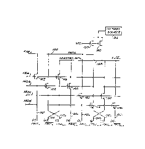
7 Figure 4 illustrates circuitry for reading information
8 in the fast port 18 and reading information in, or recording
g information from, the slow port 12 in Figure 2. The circuitry
shown in Figure 4 provides for the processing of information in
11 the slow port 12 without any interference from the reading of
12 information in the fast port 18. The circuitry shown in Figure
13 4 includes lines 60, 62, 64, 66, 68 and 72. The lines 60 and 66
14 provide signals respectively coded for logic states of "true"
and "false" in a binary bit to be processed in the slow port 12.
16 These signals are respectively indicated as "SBLn" and
17 "SBLn". Similarly, the lines 62 and 64 provide signals
1~ respectivel~ coded for logic states of "true" and "false" in a
19 binary bit to be processed in the fast port 18. These siqnals
are respectively indicated as "FBLn" and "FBLn".
21
22 The line 72 provides signals coding for the "x" word
23 to be processed in the slow port 12. These signals are
24 indicated as "SWLX". In like manner, the line 68 provides
signals coding for the "x" word to be processed in the fast port
26 18. m ese signals are indicated at "FWLX". In other words,
27 the logic levels of signals in the lines 60 and 66 indicate the
28 value of the nth bit in the x word for the slow port and the
29 lines 62 and 64 indicate the value of the nth bit in the x
word for the fast port.
31
32
`` 13037S0
1The signals on the line 60 are introduced to the
2 source of an n-transistor 75, the gate of which receives signals
3 from the line 72. The drain of the transistor 75 is connected
4 to the drain of a p-transistor 76 and to the source of an
n-transistor 78, the drain of which is connected to a suitable
6 reference potential such as a ground 80. The gates of the
7 transistors 76 and 78 have a common connection with the gate of
8 an n-transistor 82. The drain of the transistor 82 may be
9 common with the reference potential such as the ground 80. The
source of the transistor 82 is connected to the drain of an
11 n-transistor 84. The gate of the transistor 84 receives signals
12 from the line 68 and the source of the transistor 84 receives
13 signals from the line 62.
14
The line 66 is connected to the source of an
16 n-transistor 88, the gate of which receives signals from the
17 line 72. m e drain of the transistor 88 has a common connection
18 with the drain of a p-transistor 90 and the source of an
19 n-transistor 92. The source of the transistor 90 receives an
energizing potential such as approximately +5 volts from a
21 suitable voltage source 94, which is also connected to the
22 source of the transistor 76. The gates of the transistors 90
23 and 92 have a common connection with the drain of the transistor
24 76, the source of the transistor 78 and the gate of a transistor
96. The drain of the transistor 90 and the source of the
26 transistor 92 have a common connection with the gates of the
27 transistors 76 and 78. The drain of the transistor 96 is
28 connected to the reference potential such as the ground 80. The
29 source of the transistor 96 and the drain of an n-transistor 98
have a common potential. The gate of the transistor 98 receives
31
32
-- 1 0 --
.
1303750
1 the signals on the line 68 and the source of the transistor 98
2 receives the signals on the line 64.
4 ~nplifiers 97 and 99 are respectively connected to the
lines 60 and 66. The amplifiers are activated by signals on
6 "Enable" lines. When the amplifiers 97 and 99 are enabled, they
7 pass "write" signals through the amplifiers. The "write"
8 signals passing through the amplifiers 97 and 99 respectively
g represent a binary "true" and a binary "false".
11 Current sources 136 and 138 are shown in Figure 4 as
12 being connected to the lines 62 and 64. These current sources
13 correspond to transistors 136 and 138 in Figure 6. Resistors
14 124 and 126 are shown in Figure 4 as being respectively
connected from the signal generators 136 and 138 to the
16 reference potential such as ground. The resistors 124 and 126
17 are respectively shown as transistors 124 and 126 in Figure 6.
18 Resistances 93 and 95 are also respectively connected between
19 the lines 60 and 66 and the voltage source 94.
21 The transistor 84 becomes conductive when a signal of
22 high amplitude is produced on the line 68 to indicate the
23 selection of a particular word, such as the "x" word, and a high
24 signal is simultaneously produced on the line 62 (if the
transistor 82 is non-conductive) to indicate a binary value of
26 "1" for a particular bit, such as the "n" bit, in the selected
27 word. When the transistor 84 becomes conductive, current flows
28 through a circuit including the line 62, the transistor 84 and
29 the transistor 82 if the translstor 82 is conductive. This
current indicates that the particular bit in the selected word
31
32
-- 1 1 --
1:~03750
has a binary value of "1". A high gate impedance in the
2 transistor 82 isolates the current in the line 62 from the
3 reading and recording of information in the lines 60 and 66.
In like manner, current flows through a circuit
6 including the line 64, the transistor 98 and the transistor 96
7 when a signal of high amplitude is produced on the line 68 to
8 indicate the selection of a particular word such as the "x"
9 word, and a signal of high amplitude is simultaneously produced
(if the transistor 96 is conductive~ on the line 64 to indicate
11 a binary value of "0" for the bit , such as the "n" bit, in the
12 FBL line in that word. A high gate impedance in the transistor
13 96 isolates the current in the line 64 from the reading and
14 recording of information in the lines 60 and 66.
16 The operation of the circuitry shown in Figure 4 may
17 be seen from several examples. In one example, a binary value
18 of "1" may be read by the fast port 18 in Figure 1 at the "n"
19 bit of the "x" word. Under such circumstances, the transistors
84 and 98 may become conductive because of the introduction of a
21 high voltage to their gates from the 1 ine 68. Because of the
22 interconnections between the gate of each of the transistors 76
23 and 90 and the drain of the other one of such transistors, the
24 transistors 76 and 90 operate as a flip-flop. Thus, only one of
the transistors 76 and 90 can be conductive at any one time. As
26 a result, assuming that a high voltage is produced on the drain
27 of the transistor 76, a low voltage is simultaneously produced
28 on the drain of the transistor 90. The low voltage on the drain
29 of the transistor 90 prevents the transistor 82 from being
31
32
-- 12
1303750
1 conductive and prevents current from flowing through a circuit
2 including the line 62, the transistor 84 and the transistor 82.
4 me high voltage on the drain of the transistor 76 is
introduced to the gate of the transistor 96 to make the
6 transistor 96 conductive. This causes current to flow through a
7 circuit including the current source 138, the line 64, the
8 transistor 98 and the transistor 96. This current causes the
g current normally flowing through the resistance 126 from the
siqnal generator 138 to be reduced. However, the current
11 normally flowing through the current source 136 and the
12 resistance 124 continues to be maintained because of the
13 non-conductivity of the transistor 82. This causes the voltage
14 on the line 64 to be reduced relative to the voltage on the line
62. This voltage difference indicates a reading of a binary "1"
16 in the fast port 18.
17
18 In the next example, a binary "1" is read from the
19 memory 10 by the slow port 12 at the "n" bit of the "x" word.
Under such circumstances, a high voltage is introduced to the
21 gates of the transistors 75 and 88 to provde for these
22 transistors to become conductive. The resultant high voltage on
23 the drain of the transistor 75 is introduced to the gate of the
24 transistor 92 to make the transistor 92 conductive. Current
accordingly flows through a circuit including the voltage source
26 94, the resistance 35, the transistor 88 and the transistor 92.
27 The resultant voltage drop across the resistance 95 causes the
28 voltage on the line 66 to be less than the voltage on the line
29 60. This voltage difference indicates the reading of a binary
"1" by the slow port 12.
31
32
- 13 -
~303~50
1 The transistor 88 has a higher impedance than the
2 transistor 92. This causes a relatively low voltage to be
3 produced on the source of the transistor 92. This voltage is
4 introduced to the gate of the transistor 78 to make the
transistor 78 non-conductive. As a result, current cannot flow
6 through a circuit including the line 60, the transistor 75 and
7 the transistor 78. This maintains the voltage on the line 60
8 higher than the voltage on the line 66 as discussed in the
9 previous paragraph.
11 In the third example, a binary "1" is written in the
12 memory 10 by the slow port 12 at the "n" bit of the "x" word.
13 Because the "x" word is being activated, the voltage on the
14 transistor 75 is high. At this instant, the amplifiers 97 and
99 are enabled by a signal on the "enabled" line. Upon being
16 enabled, the "write" signal is introduced by the amplifier 99
17 to the line 60 as a positive voltage. At the same time, a
18 voltage having the reference such as ground is introduced to the
19 line 66 through the amplifier 99. This low voltage is
introduced to the drain of the transistor 88. A current is
21 accordingly forced by the amplifier 99 to flow through a circuit
22 including the voltage source 94, the transistor 90, the
23 transistor 88 and the line 66.
24
The high voltage on the line 60 causes the transistor
26 75 to become conductive so that a high voltage is produced on
27 the source of the transistor. m is voltage is introduced to the
28 gate of the transistor 92 to make the transistor 92 conductive.
29 Current accordingly flows through a circuit including the
voltage source 94, the transistor 90 and the transistor 92.
31
32
- 14 -
1:~037S0
Since the transistor 90 has a considerably higher impedance than
2 the transistor 92, this current flow causes the voltage on the
3 drain of the transistor 92 to have a potential approaching the
4 reference potential such as ground. This voltage is introduced
5 to the gate of the transistor 78 to maintain the transistor 78
6 non-conductive and thereby maintain the high potential on the
7 source of the transistor 75.
9 The arrangement described above is advantageous in
that the same bit of information may be simultaneously read by
11 the fast port 18 and the slow port 12. Actually, the fast port
12 18 may read the binary coded information previously recorded as
13 the value of a particular bit in the memory while the slow port
14 12 may be writing new binary coded information for that bit in
the memory.
16
17 Figure 5 illustrates circuitry for processing the
18 currents flowing in the lines 60, 62, 64 and 66 in Figures 4 and
19 5 so that the signals have a common mode and the deviations of
the signals from the common mode represent binary information.
21 The circuitry shown in Figure 5 includes the lines 60, 62, 64
22 and 66. The lines 60 and 66 are respectively connected to the
23 sources of n-transistors 120 and 122 having their drains
24 connected to the voltage source 94. Connections are
respectively made from the gates of the transistors 120 and 122
26 to the voltage source 94. The drains of the transistors 124 and
27 126 are respectively connected to the lines 62 and 64. The
28 sources of the transistors 124 and 126 receive the reference
29 potential such as the ground 80.
31
32
15 --
~0~750
1 The gates of the transistors 120 and 122 are also
2 respectively connected to gates of n-transistors 128 and 130 and
3 are further connected to receive a positive potential from the
4 voltage source 94. The sources of the transistors 128 and 130
respectively receive the signals on the lines 66 and 64. The
6 signals on the drains of the transistors 128 and 130 are
7 respectively applied to intermediate lines 132 and 134 and are
8 also respectively applied to the drains of p-transistorc 136 and
9 138. m e sources of the transistors 136 and 138 have a positive
potential such as +5 volts applied from the voltage source 94.
11 The gates of the transistors 136 and 138 have a voltage bias
12 (indicated as "VPB") applied to them to bias the transistors to
13 produce a low current.
14
The transistors 128 and 130 respectively operate as
16 cascode amplifiers. This causes a gain in the order of 1-1/2 to
17 2 to be produced in each of these cascode amplifiers when a
18 signal is introduced to a particular one of the lines 64 and 66
19 associated with that amplifier. The signal produced as a result
of the operation of the cascode amplifier 128 is introduced to
21 the line 132 and the signal produced as a result of the
22 operation of the cascode amplifier 130 is introduced to the line
23 134.
24
The transistors 136 and 138 are biased, by the
26 voltages applied to their gates, to produce a low current in the
27 transistors at all times. ~he low current in the transistor 136
28 flows through the cascode amplifier defined by the transistor
29 128 and through the transistor 124 to the reference potential
such as the ground 80, Similarly, the current through the
31
32
` ~3037S0
l transistor 138 flows through the cascode amplifier defined by
2 the transistor 130 and through the transistor 126 to the
3 reference potential such as the ground 80. The relatively low
4 currents through the transistors 124 and 126 establish a common
mode in the lines 62 and 64 to insure that noise in the lines is
6 reduced. In this way, the voltage swings in these lines from
7 the common mode represents binary information.
g The intermediate lines 132 and 134 are also shown in
Figure 6. These lines are designated in Figure 6 as "FBLCn"
ll and "FBLCn". Other corresponding pairs of lines are indicated
12 in Figure 6 at 132a and 134a, (respectively designated as
13 "FBLCn+l" and ''FBLCn+l''), 132b and 134b
14 (respectively desi~nated as "FBLCn+2" and FBLCn+2")
and 132c and 134c, ~respectively designated as "FBLCn+3"
16 and "FBLCn+3"). A plurality of channels are also
17 indicated in Figure 6 at 140a, 140b, 140c and 140d. The
18 channels 140a, 140b, 140c and 140d operate as the equivalent of
l9 an x-y matrix with the lines 132 and 134, 132a and 134a, etc.,
to select a particular bit in the memory l0.
21
22 The lines 132, 134, 132a, 134a, 132b, 134b, 132c, and
23 134c respectively have common connections with the drains of
24 p-transistors 142-156 (even numbers only). The signals in the
channel 140a are introduced to the gates of the transistors 142
26 and 146; the signals in the channel 140b are introduced to the
27 gates of the transistors 144 and 148; the signals in the channel
28 140c are introduced to the gates of the transistors 150 and 154;
29 and the signals in the channel 140d are introduced to the gates
of the transistors 152 and 156.
31
32
- 17 -
~3~3750
The drains of the transistors 142, 144, 150 and 152
2 have a common connection with a bus 154 and with the drain of a
3 p-transistor 157. Similarly, the drains of the transistors 146,
4 148, 154 and 156 have a common connection with a bus 158 and
with the drain of a p-transistor 160. me gates of the
6 transistors 157 and 160 are biased to produce a current of
7 relatively low amplitude through the transistors. A voltage is
applied to the sources of the transistors from the voltage
g source 94.
11 The circuitry of Figure 6 constitutes a switching
12 matrix. For example, when the amplitude of the signal on the
13 line 132 is high and the channel 140a is energized, current
14 flows through the bus 154 and the transistor 142. Similarly,
when a signal is produced on the line 134a to represent a binary
16 "0" and the channel 140b is activated, current flows through the
17 but 158 and transistor 148.
18
19 The transistors 157 and 160 operate in a common mode
similar to the operation of the transistors 124 and 126 in
21 Figure 5. As a result of their common mode operation, the
22 transistors 157 and 160 insure that any variations in the
23 voltages on the lines 154 and 158 represent binary coded
24 information. As will be appreciated, the signals produced in
the lines 154 and 158 represent signals read from the memory 10
26 by the fast port 10. The signals on the buses 154 and 158 are
27 respectively represented as ''FDBX'' and ''FDBX''.
28
29 The buses 154 and 158 of Figure 6 are also shown in
30 Figure 7. The synchronizing signal lines 40 and 46 of Figure 2
31
32
- 18 -
13037S0
1 are also shown in Figure 7. m e si~nals on the lines 154 and
2 158 are respectively introduced to the sources of p-transistors
3 200 and 202 and the signals on the clock line 40 are introduced
4 to the gates of these transistors. The drain of the transistor
200 has common connections with the drain of a p-transistor 204,
6 the drain of an n-transistor 206, the gate of an n-transistor
7 208 and the gate of an n-transistor 210. Similarly, connections
8 are made from the drain of the transistor 202 to the drain of a
g p-transistor 214, the drain of the transistor 208, the gate of
the transistor 206 and the gate of an n-transistor 216.
11
12 m e sources of the transistors 204 and 214 receive a
13 positive potential from the voltage source 94. The sources of
14 the transistors 206, 208, 210 and 216 have a common connection
with the drain of an n-transistor 218. The source of the
16 transistor 218 is common with the reference potential such as
17 the ground 80. The gate of the transistor 218 receives the
18 signals on the synchronizing line 40.
19
The synchronizing line 40 is also connected to the
21 gates of p-transistors 220, 222 and 224. m e sources of the
22 transistors 220, 222 and 224 receive a positive potential from
23 the voltage source 94. m e drain of the transistor 220 has
24 common connections with the gate of the transistor 214 and the
drain of the transistor 216 and with an output line 226. The
26 output line 226 is designated as ''DLX''. Output connections
27 are made from the drain of the transistor 222 to the gate of the
28 transistor 204, the drain of the transistor 210 and an output
29 line 228. m e output line 228 is designated as "DLX". The
31
32
-- 19 --
1303750
1 drain of the transistor 224 has a common connection with the
2 drain of the transistor 218.
4 When the amplitude of the clock signal on the line ~0
is 10wr the transistor 200 becomes conductive. A signal of high
6 amplitude is accordingly introduced to a line 240 common to the
7 drain of the transistor 204 and the drain of the transistor 206.
8 This signal has a higher amplitude than the signal on a line 242
9 common to the drain of the transistor 214 and the drain of the
transistor 208. m e reason is that the transistor 202 remains
11 non-conductive because of a low voltage on the line 158.
12
13 ~pon the occurrence of a positive polarity in the
14 clock signal 50 on the line 40, the transistor 218 becomes
conductive because of the introduction of the synchronizing
16 signal to the gate of the transistor. This causes the voltage
17 on the drain of the transistor 218 to decrease to substantially
18 the reference potential such as the ground 80. Because of the
19 high potentia] on the line 240, the transistor 208 becomes
conductive and produces on its drain a potential approaching the
21 reference potential such as the ground 80. This voltase is
22 introduced to the gate of the transistor 206 to insure that the
23 transistor 206 will remain non-conductive.
24
When the voltage on the drain of the transistor 218
26 approaches the reference potential such as the ground 80, the
27 transistor 210 becomes conductive because of the introduction of
28 the high voltage to its gate from the line 240. This causes the
29 voltage on the bus 228 to approach the reference potential such
as ground. The resultant reference potential, such as the
31
32
- 20 -
1303~50
1 ground 80, on the gate of the transistor 204 causes the
2 transistor 204 to become conductive. This prolongs a voltage of
3 high amplitude on the line 240 and insures that the transistors
4 208 and 210 will be strongly conductive.
6 In the next half cycle (the negative half cycle) of
7 the synchronizing (or clock) signal 50 on the line 40, the
8 transistors 220, 222 and 224 become conductive. When the
g transistors 220 and 222 become conductive, they introduce the
same voltages (the voltage from the voltage source 94) to the
11 lines 226 and 228 to assure that any difference in the
12 potentials on these lines in the previous half cycle of the
13 synchronizing signal is eliminated. This insures that a
14 considerable difference in potential will be produced in the
lines 226 and 228 in the subsequent half cycle (the positive
16 half cycle) of the synchronizin~ signals on the line 40. When
17 the transistor 224 becomes conductive in the negative half cycle
18 of the synchronizing signal 50 on the line 40, it provides a
19 positive voltage to the source of the transistor 218 to insure
that the transistor will become conductive in the subsequent
21 half cycle (the positive half cycle) of the clock siqnals.
22
23 When a positive signal is produced on the line 158 to
24 indicate a binary value of "0", the signal on the line 242 has a
higher amplitude than the signal on the line 240 during the
26 negative half cycle of the synchronizing signal 50 on the line
27 40. As a result, when the transistor 218 becomes conductive in
28 the next half cycle (the positive half cycle) of the
29 synchronizing signal 50, the transistors 206 and 210 become
31
32
- 21 -
0~750
1 conductive and the voltage on the line 226 approaches the
2 reference potential such as the ground 80.
4 The circuitry shown in detail in Figure 7 and
described above is duplicated in second stages which are
6 included within a box generally indicated at 250 and shown in
7 the broken lines in Figure 7. However, the stages 250 receive
8 the synchronizing signals 52 on the clock line 46. Since these
9 signals are displaced by 180 in phase from the synchronizing
signals 50 on the line 46, the signals produced on output lines
11 252 and 254 are displaced in phase by 180 from the signals
12 produced on the lines 226 and 228. The signals on the output
13 lines 252 and 254 are respectively indicated as ''DRX'' and
14 ''DRX'' in Figure 7. In other words, the signals produced in
the lines 154 and 158 in one half cycle of the synchronizing
16 signals 46 in Figure 1 in the stage 250 are sampled while the
17 signals produced on the lines 154 and 158 in the previous half
18 cycles of the synchroni~ing signals 46 are evaluated in the
19 output lines 226 and 228. In the next half of the synchronizing
signals 46, the signals sampled in the stage 250 are evaluated
21 in the output lines 226 and 228 while the stage shown in detail
22 in Figure 7 is sampling the signals on the lines 226 and 228.
23
24 The circuitry shown in Figure 8 includes the lines 226
and 228 and the lines 252 and 254. The lines 226, 228, 252 and
26 254 are respectively connected to the gates of transistors 270
27 and 272, the gates of transistors 274 and 276, the gates of
28 transistors 278 and 280 and the gates of transistors 282 and
29 284. m e transistors 270 and 278 are n-transistors and the
transistors 272, 274, 276, 280, 282 and 284 are p-transistors.
31
32
- 1303750
1 Connections are also respectively made from the lines 226 and
2 228 to the drains of the transistor 272 and the drains of the
3 transistor 278. Similarly, the lines 252 and 254 are
4 respectively connected to the drains of the transistors 280 and
284.
7 m e sources of the transistors 272, 274, 276, 280, 282
8 and 284 receive a positive potential such as +5 volts from the
9 voltage source 94. The drains of the transistors 274 and 282
are respectively common with the drains of the transistors 270
11 and 278. A resultant line 288 extends from a common connection
12 between the drains of the transistors 270, 274, 278 and 282.
13
14 A signal of low amplitude is produced on only one of
the lines 226, 228, 252 and 254 at any time to represent binary
16 coded information and signals of relatively high amplitude are
17 simultaneously produced on the other ones of the output lines
18 226, 228, 252 and 254. By way of illustration, a signal of low
19 amplitude may be produced on the line 226 and a signal of high
amplitude may be simultaneously produced on the lines 228, 252
21 and 254. When the amplitude of the signal on the line 226 is
22 low, it introduces a low voltage to the source of the transistor
23 278. At the same time, a signal of high voltage is introduced
24 to the gate of the transistor 278 from the line 252. This
causes the transistor 278 to become conductive so that the
26 voltage on the drain of the transistor approximates the voltage
27 on the source of the transistor and a signal of low amplitude is
28 produced on the resultant line 288. The low voltage on the
29 drain of the transistor 278 also appears on the drains of the
31
32
1303750
1 transistors 274 and 282 and the drain of the transistor 270 and
2 prevents these transistors from becoming conductive.
4 To insure the operation of the transistors 270, 274,
278 and 282 as discussed a~ove, the signals on the lines 226 and
6 228 are respectively introduced to the transistors 272 and 276.
7 These signals prevent the transistor 272 from becoming
8 conductive and cause the transistor 276 to become conductive.
g This causes a high voltage to be produced on the drain of the
transistor 276 and to be introduced to the gate of the
11 transistor 274 to prevent the transistor 274 from becoming
12 conductive.
13
14 It may sometimes happen that a signal of low amplitude
is produced on the line 228. At the same time, signals of high
16 amplitude are produced on the lines 226, 252 and 254. m e
17 signal of low amplitude on the line 228 is introduced to the
18 gate of the transistor 274 to make the transistor conductive.
19 This causes the drain of the transistor 274 to have a high
voltage, this voltage being introduced to the resultant line
21 288. At the same time, the transistors 270 and 278 are not
22 conductive. The reason is that each of these transistors has
23 the same voltage on its gate and its source because of the high
24 voltages on the lines 226 and 252. The transistor 282 is not
conductive because a high voltage is introduced to its gate from
26 the line 254.
27
28 The transistors 272 and 276 operate to insure that the
29 transistors 270, 274, 278 and 282 will operate as discussed in
the previous paragraphs when the line 228 has a signal of low
31
32
13037S0
1 amplitude and the lines 226, 252 and 254 have signals of hi~h
2 amplitude. These signals prevent the transistor 276 from become
3 conductive and cause the transistor 272 to become conductive.
4 The resultant high voltage on the drain of the transistor 272
insures that the transistor 270 will remain non-conductive.
7 As will be seen, the circuit shown in Figure 8 is
8 symmetrical in that the lines 226 and 252 have the same
9 connections and the lines 228 and 254 have the same
connections. As a result, the discussion above with respect to
11 the introduction of a signal of low amplitude on the line 226 is
12 applicable to the introduction of a signal of low amplitude on
13 the line 252. Similarly, the discussion above with respect to
14 the introduction of a signal on the line 228 is also applicable
to the introduction of a signal on the line 254.
16
17 The system described herein h~s certain important
18 advantages. It provides for the reading of binary coded
19 information from the memory 10 by the fast port 18 at the same
time that binary coded information is read from, or written
21 into, the memory 10 by the slow port 12. The simultaneous
22 transducing action is obtained by the fast port 18 and the slow
23 port l2 without obtaining any interference between the actions
24 of the fast and slow ports. This results from the operation of
the circuitry shown in ~igure 4 and described above. Actually,
26 both the fast port 18 and the slow port 12 may simultaneously
27 read the same bit of information from the memory.
28
29 The system also has other important
advantages. It provides for the readinq of binary coded
31 information by the fast port 18 on a synchronous basis with
32
~303750
1 signals from the clock signal generator 30 but provides for the
2 reading or writing of binary coded information by the slow port
3 12 on an asynchronous basis relative to the clock signals. mis
4 synchronous-asynchronous relationship between the operation of
the fast port 18 and the slow port 12 is especially significant
6 because the reading of binary coded information from the fast
7 port 18 occurs at a high frequency such as approximately one
8 hundred and twenty five megahertz (125 mhz).
The operation of the fast port 18 also offers other
11 important advantages in addition to those specified above. For
12 example, the fast port 18 reads binary coded information from
13 the random access memory 10 in each half cycle of the
14 synchronizing signals 50 and 52 shown in Figure 3. The fast
port 18 samples, in a first stage, first bits of such binary
16 coded information in the negative half cycles of the
17 synchronizing signals 50 and evaluates the sampled information
18 in the positive half cycles of the such synchronizing signals.
19 The fast port 18 samples, in a second stage identical in
construction to the first stage, second bits of such binary
21 coded information in the positive half cycles of the
22 signals 52 and evaluates such sampled information in the
23 negative half cycles of such synchronizing signals.
24
In this way, the frequency of the fast port 18 in
26 reading binary coded information from the memory 10 is
27 effectively doubled without any loss in the ability to read such
28 information. The stages (Figure 7) sampling and evaluating the
29 binary coded information read by the fast port 18 from the
memory 10 also operate advantageously in prolonging the
31
32
- 26 -
13~ 7SO
1 evaluation of the sampled signals in the next half cycles after
2 each such sampling. The circuitry shown in Figure 8 then
3 introduces such evaluated signals to the resultant line 288 on
4 an exclusive basis whereby the signal from only one of the
output lines 226, 228, 252, and 254 can be introduced to the
6 resultant line at each instant.
8 Although this invention has been disclosed and
9 illustrated with reference to particular embodiments, the
principles involved are susceptible for use in numerous other
11 embodiments which will be apparent to persons skilled in the
12 art. The invention is, therefore, to be limited only as
13 indicated by the scope of the appended claims.
14
16
17
18
19
21
22
23
24
26
27
28
29
31
32
- 27 -