Note: Descriptions are shown in the official language in which they were submitted.
~3~333
LIGHT RECEIVING ME~ER FOR USE
IN ELECTROPHOTOGRAPHY
FIELD OF THE INVENTION
Thls inventlon relates to an improved light receiving
men~er for use in electrophotography which is sensitive
to electromag~etic waves such as light (which herein means
in a broader sense those lights such as ultra-violet rays,
visible rays, infrared rays, X-rays and y-rays).
~`; :
.
BACKGROUND OF THE INVENTION
For~the photoconductive material to constitute a llght
receiving layer in a light receiving mçmber~for use in
electrophotography, it is required to be highly sensitive,
to have a hlgh SN ratio [photocurrent (Ip)/dark current (Id)],
~to have absorption spectrum characteristics suited for the
spectrum characteristics of an electromagnetic wave to be
rradlated,~ to be quickly responsive and to have a desired
dark reslstance. It is also requlred to be not harmful to
livlng~things as well as man upon the use.
Especially, in the case where lt is the llght receiving
member to be applied in an electrophotographic machine for
use in office, causing no pollution is indeed important.
1 ~o
.
~1 3~38~3
From these standpoints, the public attention has been
focused on light receiving members comprising amoxphous
materials con~aining silicon atoms (hereinafter referred
to as "a-Si"), for example, as disclosed in Offenlegungsschriftes
Nos. 2746967 and 2855718 which disclose use of the light
receiving member as an image-forming member in electro-
photography.
For the conventional light receiving members comprising
a-Si materials, there have been made improvements in their
optical, electric and photoconductive characteristics such
as dark resistance, photosensitivity, and photoresponsiveness,
use-environmental characteristics, economic stability and
durability.
Howeuer, there are still left subjects to make further
improvements in their characteristics in the synthesis
situation ln order to make such light receiving member
practically usable.
For example, in the case where such conventional light
receiving member is employed in the light receiving member
for use in electrophotography with aiming at heightening the
photosensitivity and dark resistance, there are often observed
a residual voltage on the conventional light receiving
member upon the use, and when:it is repeatedly used for a
long period of time, fatlgues due to the repeated use wlll
be accumulated to cause the so-called ghost phenomena
38~3
inviting residual images.
Further, in the prepara-tion o~ the light receiving
layer of khe conventional light receiving member for use
in electrophotography using an a-Si material, hydrogen atoms,
halogen atoms such as fluorine atoms or chlorine atoms,
elements for controlling the electrical conduction type such
as boron atoms or phosphorus atoms, or other kinds of a-toms
for improving the characteristics are selectively incorporated
in the light receiving layer.
However, the resulting light receiving layer sometimes
becomes accompanied with defects on the electrical character-
istics, photoconductive characteristics and/or breakdown
voltage according to the way of the incorporation of said
constituents to be employed.
That is, in the case of using the light receiving member
having such light receiving layer, the life of a photocarrier
generated in the layer with the irradiation of light is not-
sufficient, the inhibition of a charge injection from the
side of the substrate in a dark layer region is not sufficiently
carried out, and image defects likely due to a local break-
down phenomenon which is so-called "white oval marks on
half-tone copies" or other image defects likely due to
abraslon upon using a blade for the cleaning which is
so-called "white line" are apt to appear on the transferred
images on a paper sheet.
q~3~913
Further, in the case where -the above light receiving
member is used in a much moist atmosphere, or in the case
where after being placed in that atmosphere it is used,
the so-called "image flow" sometimes appears on the
transferred images on a paper sheet.
In consequence, it is necessitated not only to make
a further improvement in an a-Si material itself but also to
establish such a light receiving member not to invite any of
the foregoing problems.
SU~MARY OF THE INVENTION
The object of this invention is to provide a light
receiving member for use in electrophotography which has
a light receiving layer free from the foregoing problems and
capable of satisfying various kind of requirements in electro-
photography.
That is, the main object of this invention is to
provide a light receiving member for use in electrophototog-
raphy which has a light receiving layer comprising a layer
formed of a-Si and a layer formed of a polycrystal material
containing silicon atoms (hereinafter referred to as "poly-Si"),
that electrical~ optical and photoconductive properties are
always substantially stable scarcely depending on the working
circumstances, and that is excellent against optical fatigue,
~L3~ 519~
causes no ~egradation upon repeating use, excellent in
durability and moisture-proofness and exhibits no or scarce
residual voltage.
Another object of this invention is to provide a light
receiving member for use in electrophotography which has a
light receiving layer comprising a layer formed of a-Si and
a layer formed of poly-Si, which is excellent in the close
bondability with a substrate on which the layer is disposed
or between the laminated layers, dense and stable in view
of the structuralarrangement and is of high quality.
~ further object of this invention is to provide a
light receiving member for use in electrophotography which
has a light receiving layer comprising a layer formed of
a-Si and a layer formed of poly-Si, which exhiblts a suf-
ficient charge-maintaining function in the electrification
process of forming electrostatic latent images and excellent
electrophotographic characteristics when it is used in
electrophotographic method.
A still further object of this invention is to provide
a light receiving member for use in electrophotography which
has a light receiving layer comprising a layer formed of a-Si
and a layer formed of poly-Si, which invites neither an
image defect nor an image flow on the resulting visible
images on a paper sheet upon repeated use in a long period
of time and which gives highly resolved visible images with
3~93
clearer half-tone which are highly dense and quality.
Other object of this invention is to provide a light
receiving member for use in electrophotography which has a
light receiving layer comprising a layer formed of a-Si and
a layer formed of poly Si, which has a high photosensitivity,
high S/N ratio and high electrical voltage withstanding
property.
In order to overcome the foregoing problems'on the
conventional light receiving member for use in electro-
photography and attaining the above-mentioned objects, the
present inventors have made various studies while forcusing
on its surface layer and other constituent layer. As a
result, the present inventors have found that when the
surface layer is formed of an amorphous material containing
silicon atoms, carbon atoms and hydrogen atoms and the content
of the hydrogen atoms is controlled to be in the range between
41 and 70 atomic %, and that when the absorption layer for
light of long wavelength ~hereinafter referred to as t~ IR
layer;') as one of other,constitu~nt layers except the surface
layer is lormed of a polycrystal material containing silicon
atoms and germanium atoms, those problems on the conventional
light receiving member for use in electrophotography can be
satisfactorily eliminated and the above-mentioned objects
can be effectively attained.
Accoxdingly, one aspect of this invention is to provide
i3~ 3
an improved light receiving member for use in electrophoto-
graphy comprising a substrate usable for electrophotography
and a light receiving layer constituted with an IR layer
formed of a polycrystal material containing silicon atoms
and germanium atoms, and if necessary, hydrogen atoms or/and
halogen atoms ~hereinafter referred to as "poly-SiGe(H,X~"],
a photoconductive layer formed of an amorphous material
containing silicon atoms as the main constituent atoms and
at least one kind selected from hydrogen atoms and halogen
atoms [hereinafter referred to as "A-Si(H,X)"], and a surface
layer having a free surface being formed of an amorphous
material containing silicon atoms, carbon atoms and hydrogen
atoms (hereinafter referred to as "A-Si:C:H") in which the
amount of the hydrogen atoms to be contalned is ranging from
41 to 70 atomic ~.
Another aspect of this invention is to provide an improved
light receiving member for use in electrophotography CQmpriSing
a substrate usable for electrophotography and a light receiv-
ing layer constituted with an IR layer formed of a poly-SiGe(H,X),
a charge injection inhibition layer formed of an A-Si~H,X)
containing an element for controlling the conductivity [herein-
after referred to as ~'A-SiN(H,X)"], wherein M represents an
element for controlling the conductivity, a photoconductive
layer formed of an A-Si(H,X), and a surface layer havlng a
free surface being formed of an A-Si:C:H in which the amount
~3~ 3
of the hydrogen atoms to be contained is ranging from 41 to
70 atomic %.
It is also possible for the light receiving member
according to this invention to have a con-tact layer, which
is formed of an amorphous material or a polycrystal material
containing silicon atoms as the main constituent atoms and
at least one kind selected from nitrogen atoms, oxygen atoms
and carbon atoms [hereinafter referred to as "A-Si(N,O,C)"
or "poly-Si~N,O,C)"], between the substrate and the IR layer
or between the substrate and the charge injection inhibition
layer.
And the above-mentioned photoconductlve layer may contain
one or more kinds selected from oxygen atoms, nitrogen atoms,
and an element for controlling the conductivity as the layer
constituent atoms.
The above-mentioned charge injection inhibition layer
may contain at least one kind selected from nitrogen atoms,
oxygen atoms and carbon atoms as the layer constituent atoms.
The above-mentioned IR layer may contain one or more
kinds selected from nitrogen atoms, oxygen atoms, carbon
atoms, and an element for controlling the conductivity as
the layer constituent atoms.
The light receiving member having the above-mentioned
light receiving layer for use in electrophotography according
to this invention is free from the foreging problems on the
~3~38g3
conventional light receiving members for use in electro-
photography, has a wealth of practically applicable
excellent electric, optical and phtoconductive character-
istics and is accompanied with an excellent durability and
satisfactoxy use environmental characteristics.
Particularly, the light receiving member for use in
electrophotography according to this invention has substan-
tially stable electric characteristics without depending
on the working circumstances, maintains a high photosensi-
tivity and a high S/N ratio and does not invite any
undesirable influence due to residual voltage even when it
is repeatedly used for along period of time. In addition,
it has sufficient moi~tu;r~ registant and optical fatigue
resistance, and cauF,c~ neither degradation upon repeating
use nor any defect on breakdown voltage.
Because of this, according to the light receiving
member for use in electrophotography of this invention,
even upon repeated use for a long period of time, highly
resolved visible images with clearer half tone which are
highly dense and quality are stably obtained.
BRIEF DESCRIPTION OF THE DRAWINGS
Figure l(A) through Figure l~D) are schematic views
illustrating the typical layer constitution of a representative
~L3~ 393
light receiving member for use in electrophotography
according to this invention ; -
Figure 2 through Figure 7 are views illustrating the
thicknesswise distribution of germanium atoms in the IR
layer ;
Figure 8 through Figure 12 are views illustrating the
thicknesswise distribution of the group III atoms or the
group V atoms in the charge injection inhibition layer;
Figure 13 through Figure 19 are views illustrating the
thicknesswise distribution of at least one kind selected from
nitrogen atoms, oxygen atoms, and carbon atoms in the charge
injection inhibition layer.i
Figure 20(A) through Figure 20(C) are schematlc views
for examples of the shape at the surface of the substrate in
the light receiving member for use in electrophotography
according to this invention ;
Figure 21 is a schematic view for a preferred example
of the light receiving member for use in electrophotography
: ~ :according to this invention which has a light receiving layer
as shown in Figure l(C) formed on the substrate having a
preferred surface ;
Figures 22 through 23 are schematic explanatory views
: ~of a preferred method for preparing the substrate havinq -the
preferred surface:used in the light receiving member shown
in Figure 21 ;
~L3~113~93
Figure 24 is a schematic explanatory view of a fabrica-
tion apparatus for preparing the light receiving member for
use in electrophotography according to this invention;
Figure 25 and Figure 26 are schematic views respectively
illustrating the shape of the surface of the substrate in
the light receiving member in Bxamples 9 and 21, and Examples
10 and 22;
Figure 27 is a view illustrating the thicknesswise
distribution of germanium atoms in the IR layer in Example 2;
and
Figure 28 is a view illustrating the thicknesswise
distribution of boron atoms and oxygen atoms in the charge
injection inhibition layer and of germanium atoms in IR
layer in Example 12.
DETAILED DESCRIPTION OF THE INVENTION
Representative embodiments of the light receiving
member for use in electrophotography according to this
.invention will now be explained more specifically refer-
ring to the drawings. The description is not intended to
limit the scope of this invention.
Representative light receiving members for use in
electrophotography according to this invention are as shown
in Figure l(A) through Figure l(D), in which are shown
~3~3~193
light receiving layer 100, substrate 101, IR layer 102,
photoconductive layer 103, surface layer 104, free surface
105, charge injection inhibition layer 106, and contact layer
107.
Figure l(A) is a schematic view illustrating a typical
representative layer constitution of this invention, in
which is shown the light receiving member comprising the
substrate 101 and the light receiving layer 100 constituted
by the IR layer 102, the photoconductive layer 103 and the
sur~ace layer 104.
Figure l(B) is a schematic view illustrating another
representative layer constitution of this invention, in
which is shown the light receiving member comprising the
substrate 101 and the light receiving layer 100 constituted
by the IR layer 102, the charge injection inhibition layer
106, the photoconductive layer 103 and the surface layer 104.
Figure l(C) is a schematlc view illustrating another
representative layer constitution of this invention, in which
is shown the light receiving member comprising the substrate
101 and the light receiving layer 100 constituted by the
contact layer 107, the IR layer 102, the charge injection
inhibition layer 106, the photoconductive layer 103 and
the surface layer 104.
Figure l(D) is a schematic view illustrating another
representative layer constitution of this invention, in
12
~ 3~3~93
which is shown the light receiving member comprising the
substrate lOl and the light receiving layer constituted by
the contact layer 107, the I~ layer 102, the photoconductive
layer 103 and the surface layer 104.
Now, explanation will be made for the substrate and
each constituent layer in the light receiving member of
this invention.
Substrate lOl
The substrate lOl for use in this inventîon may either
beelecb~conductive or insulative. The electroconductive
support can include, for example, metals such as NiCr,
stainless steels, Al, Cr, Mo, Au, Nb, Ta, V, Ti, Pt and Pb
or the alloys thereof.
The electrically insulative support can include, for
example, films or sheets of synthetic resins such as
polyester, polyethylene, polycarbonate, cellulose acetate,
polypropylene, polyvinyl chloride, polyvinylidene chloride,
polystyrene, and polyamide, glass, ceramic and paper. It
is preferred that the electrically insulative substrate is
applied with electroconductive treatment to at least one of
the surfaces thereof and disposed with a light receiving
layer on the thus treated surface.
In the case of glass, for instance, electroconductivity
is applied by disposing, at the surface thereof, a thin
~ ~03~3
film made of NiCr, Al, Cr, L~o, Au, Ir, Nb, Ta, V, Ti, Pt,
Pd, In203, SnO2, ITO (In203 + SnO2), etc. [n the case of
the synthetic resin film such as a polyester film, the
electroconductivity is provided to the surface by disposing
a thin film of metal such as NiCr, Al, Ag, Pv, Zn, Ni, Au,
Cr, Mo, Ir, Nb, Ta, V, Tl and Pt by means of vacuum
deposition, electron beam vapor deposition, sputtering,
etc., or applying lamination with the metal to the surface.
The substrate may be of any configuration such as cylindrical,
belt-like or plate-like shape, which can be properly determined
depending on the application uses. For instance, in the
case of using the light receiving member shown in Figure l
in continuous high speed reproduction, it is desirably
configurated into an endless belt or cylindrical form.
The thickness of the support member is properly
determined so that the light receiv~ng member as desired can
be formed.
In the case where flexibility is required for the light
receiving member, it can be made as thin as possible within
a range capable of sufficiently providing -the function as
the substrate. ~owever,~the ~hickness is usually greater
than lO ~m in vie~ of the fabrication and handling or mechanical
strength of the substrate.
And, it is possible for the surface of the substrate
to be uneven in order to eliminate occurrence of defective
14
~ ~31J13~3~3
images caused by a so-called interference fringe pattern
being apt to appear in the formed images in the case where
the image ~ormation is carried out using coherent mono-
chromatic light such as laser beams.
In that case, the uneven surface shape of the substrate
can be formed by the grinding work with means of an
appropriate cutting tool, for example, having a V-form bite.
~ hat is, said cutting tool is firstly fixed to the
predetermined position of milling machine or lathe, then,
for example, a cylindrical substrate is moved regularly in
the predeter~ined direction while being rotated in accordance
with the predetermined program to thereby obtain a surface-
treated cylindrical substrate of a surface having irregular-
ities in reverse V-form with a desirably pitch and depth.
The irregularities thus formed at the surface of the
cylindrical substrate form a helical structure along the
center axis of the cylindrical substrate~ The helical structure
making the reverse V-form irregularities or the surface of
the cylindrical substrate may be double or treble. Or
otherwise, it may be of a cross-helical structure.
Further, the irregularities at the surface of the
cylindrical substrate may be composed of said helical
structure and a delay line formed along the center axis of
the cylindrical substrate. The cross-sectional form of the
convex of the irregularity formed at the substrate surface
~ 3~3~3~3
is in a reverse V-form in order to attain controlled uneven-
ness of the layer thickness in the minute column for each
layer to be formed and secure desired close bondability
and electric contact between the substrate and the layer
formed directly thereon.
And as shown in Figure 20, it is desirable for the
reverse V-form to be an equilateral triangle, right~angled
triangle or inequilateral triangle. Among these triangle
forms, equilateral triangle form and right-angled triangle
form are most preferred.
Each dimension of the irregularities to be formed
at the substrate surface under the controlled conditlons
is properly determined having a due regard on the following
polnts .
That is, firstly, a layer composed of, for example,
a-Si(H,X) or poly-Si(H,X) to constitute a light receiving
layer is structurally sensitive to the surface state of
the layer to be formed and the layer quality is apt to
largely change in accordance wlth the surface state.
Therefore, it is necessary for the dimention of the
irregularity to be formed at the substrate surface to be
determined not to invite any decrease in the layer quality.
Secondly, should there exist extreme irregularities
on the free surface of the light receiving layer, cleaning
in the cleaning process after the formation of visible images
16
~ 3~3~393
becomes difficult to sufficiently carry out. In addition,
in the case of carrying out the cleaning with a blade,
the blade will be soon damaged.
From the viewpoints of avoiding the problems
in the layer formation and the electrophotographic processes,
and from the conditions to prevent occurrence of the problems
due to interference fringe patterns, the pitch of the
irregularity to be formed at the substrate surface is
preferably 0.3 to 500 ~m, more preferably 1.0 to 200~m, and,
most preferably, 5.0 to 50 ~m.
As for the maximum depth of the irregularity, i-t is
preferably 0.1 to 5.0 ~m, more preferably 0.3 to 3. b ~m,
and, most preferably, 0.~ to 2.0 ~m.
And when the pitch and the depth of the irregularity
lie respectively in the above-mentioned range, the inclina-
tion of the slope of the dent (or the linear convex) of the
irregularity is preferably 1 to 20, more preferably 3 to
15, and, most preferably, 4 to 10.
Further, as for the maximum figure of a thickness
difference based on the ununiformity in the layer thickness
of each layer to be formed on such substrate surface, in
the meaning within th~ same pitch, it is pxeferably 0.1 to
2.0 ~m, more preferably 0.1 to l.5 ~m, and, most preferably,
0.2 ~m to 1.0 ~m.
In alternative, the irregularity at the substrate
~ 3~3~3
surface may be composed of a plurality of fine spherical
dimples which are more effective in eliminating the occur-
rence of defective images caused by the interference
fringe patterns especially in the case of using coherent
monochromatic light such as laser beams.
In that case, the scale of each of the irregularities
composed of a plurality of fine spherical dimples is smaller
than the resolving power required for the light receiving
member for use in electrophotography.
A typical method of forming the irregularities composed
of a plurality of fine spherical dimples at the substrate
surface will be hereunder explained referring to Figures
22 and23.
Figure 22 is a schematic view for a typical example
of the shape at the surface of the substrate in the light
receiving member for use in electrophotography according
to this invention, in which a portion of the uneven shape
is enlarged. In Figure 22, are shown a support 2201, a
support surface 2202, a rigid true sphere 2203, and a
spherical dimple 2204.
Figure 22 also shows an example of the preferred methods
of preparing the surface shape as mentioned above. That
is, the rigid true sphere 2203 is caused to fall gravitationally
from a position at a predeter~ined height above the substrate
surface 2202 and collide against the substrate surface 2202
.
18
~ 3~3893
to thereby form the spherical dimple 2204. A plurality of
fine spherical dimples 2204 each substantially of an identical
radius of curvature R and of an identical width D can be
formed to -the substrate surface 2202 by causing a plurality
of rigid true spheres 2203 substantially of an identical
diameter R' to fall from identical height h simultaneously
or sequentially.
Figure 23 shows a typical embodiment of a substrate
formed with the uneven shape composed of a plurality of
spherical dimples at the surface as described above.
In the embodiment shown in Figure 23, a plurality of
dimples pits 2304, 2304 ... substantially of an identical
radius of curvature and substantially of an identical width
are formed while heing closely overlapped with each other
thereby forming an uneven shape regularly by causing to fall
a plurality of spheres 2303, 2303, ... regularly and
substantially from an identical height to different positions
at the surface 2302 of the support 2301. In this case, it
lS naturally required for forming the dimples 2304, 2304 ...
overIapped with each other that the spheres 2303, 2303 ...
are gravlationally dropped such that the times of collision
of the respective spheres 2303 to the support 2302 and
displaced from each other.
By the way, the radius of curvature R and the width D
of the uneven shape forr~ed by the spherical di~ples at -the
19
~1 3~3893
substrate surface of the light receiving member fur use in
electrophotography according to this invention constitute
an important factor for effectively attaining the advantageous
effect of preventing occurrence of the interference fringe
in the light receiving member for use in electrophotography
according to this inventlon. The present inventors carried
out various experiments and, as a result, found the following
facts.
~ hat is, if the radius of curvature R and the width D
satisfy the follo~ing equa-tion:
D ~ 0.035
0.5 or more Newton rings due to the sharing interference are
present in each of the dimples. Further, if they satisfy
the following equation:
D ~ 0 055
one or more Newton rings due to the sharing interference
are present in each of the dimples.
From the foregoing, it is pre~erred that the ratio D/R
is greater than 0.035 and, preferably, greater than 0.055
for dispersing the interference fringes resulted throughout
the light receiving ~e~ber in each of the dimples thereby
preventing occurrence of the interference fringe in the
light receiving member.
Further, it is desired that the width D of the unevenness
~1 3~ 313
formed by the scraped dimple is about 500 ~m at the maximum,
preferably, less than 200 ~m and, r~ore preferably less than
lûO llm
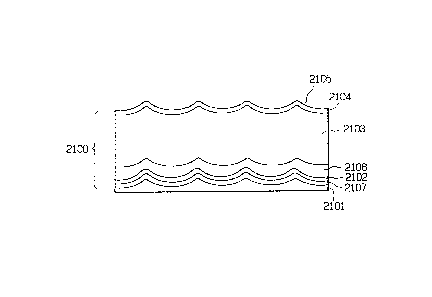
Figure 21 is a schemati~ view illustrating a represen-
tative ernbodiment of the light receiving mernber in which
is shown the light receiving member comprising the above-
mentioned substrate 2101 and the light receiving layer 2100
constituted by contact layer 2107, IR layer 2102~ charge
injection inhibition layer 2106, photoconductive layer 2103,
and surface layer ~104 having free surface 2105.For thls light
receiving mernber for use in electrophotography, since the radius
of curvature of the spherical dimples formed at the interface
in the light receiving later 2100~is not identical with that
formed at the free sur~ace 2105, the reflection light at the
interface and the reflection light at the free surface have
reflection angles different from each other. Because of this,
a sharing interference corresponding to the so-called Newton
ring phenornenon occurs and the interference fringe is dispersed
within the dimples. Then, if the interference ring should appear
in the microscopic point of view in the images caused by way
of the light receiving member, it is not visually recognized.
That ~i5, in the light receiving member having the light
~receiving layer of multi-layered structure 2100 formed on the
substrate having ~such a surface 2101, lights passing through
the light receiving layer 2100 reflect on the layer interface
21
~3~g3
and at the substrate surface and interfer each other to
thereby effectively prevent the resulting images from being
accompanied with infringe patterns.
IR Layer 102 (or 21G2)
In the light receiving member for use in electrophotog-
raphy of this invention, the I~ layer is formed of
poly-SiGe(li,X) ~ `
~ s for the germanium atoms to be contained in the IR
layer, they may be distr~buted uniformly in its entire
layer region or unevenly in the direction toward the layer
thickness of its entire layer region.
However, in any case, it is necessary for the germanium
atoms to be distributed uniformly in the direction parallel
to the~surface of the substrate ln order to provlde the
uniformness of the characterlstics to be brought out
tHerein or hereinafter, the uniform distribution means
that the distribution of germanium atoms in the layer is
uniform both in the directlon parallel to the surface of
the substrate and in the thlckness dlrection The uneven
distribution means that the distribution of germanium atoms
in the layer is uniform in the dlrection parallel to the
surface of the substrate but is uneven in the thickness
direction. 1 ~ ~
'l`hat is, in tl1e case wheL^e the c3ermanium atoms are
contained une~enly in the direction toward tl-e layer thickness
of its entire layer region, the germanium atoms are incorpo-
rated so as to be in the skate that these atoms are more
largely distributed in the layer region near the substxate
than in the layer apart from the substrate ~namely in the
layer region near the free surface of the light receiving
layer) or in the state opposite to the above state.
In preferred embodiments, the germanium atoms~are
contained unevenly in the direction toward the layer thick-
ness of the entire layer region of the IR layer.
In one of the preferred embodiments, the germanium atoms
are contained in such state -that the distributing concentra-
tion of these atoms is changed in the way of being decreased
from the layer region near the substrate toward the layer
region near the charge injection lnhibition layer. In this
case, the affinity between the IR layer and the charge
injectlon inhibition becomes excellent. And, as later
detailed, when the distributing concentration of the germanium
atoms is made significantly large in the layer region adjacent
to the substrate, the IR layer becomes to substantially and
completely absorb the light of long wavelength that can
be hardly absorbed by the photoconductive layer in the case
of using a semiconductor laser as the light source. ~s a
result, the occurrence of the interference caused by the
light reflection from the surface of the substrate can be
effectively prevented.
23
~ 3~3~19;1
Explanation will be made to the typical embodiments
of the distribution of germanium atoms to be contained
unevenly in the direction toward the layer thickness of
the IR layer while referring to Figures 2 through 7 showing
the distribution of germanium atoms. ~owever, this invention
is no way limited only to these embodiments.
In Figures 2 through 7, the abscissa represent the
distribution concentration C of germanium atoms and the
ordinate represents the thickness of the IR layer; and tB
represents the extreme position of the IR layer containing
germanium atoms is formed from the tB side toward the tT side.
Figure 2 shows the first typical example of the thickness-
wise distribution of the germanium atoms in the IR layer.
In this example, germanium atoms are distributed such that
the concentration C remains constant at a value Cl in the
range from position tB ~at which the IR layer comes into
contact with the substrate) to position tl, and the concen-
tration C gradually and continyously decreases from C2 in the
range from position tl to position tT/ where the concentration
of the germanium atoms is C3.
In the example shown in Figure 3, the distribution
concentration C of the germanium atoms contained in the IR
layer is such that concentration C4 at position tB continuously
decreases to concentration C5 at position tT~
In the example shown in Figure 4, the distribution
24
~3(~ 93
concentration C of the germanium atoms is such that the
concentration C6 remains constant in the range from
position tB and position t2 and it gradually and continyously
decreases in the range from position t2 and position tT.
The concentration at position tT is substantially ~ero.
("Substantially zero" means that the concentration is lower
than the detectable limit.)
In the example shown in Figure 5, the distribution
concentration C of the germanium atoms is such that concen-
tration C8 gradually and continuously decreases in the range
from position tB and position tT, at which it is substantially
zero.
In the example shown in Figure 6, the distribution
concentration C of the germanium atoms is such that concen-
tration Cg remains constant in the range from position tB
to position t3, and concentration Cg linearly decreases to
concentration C10 in the range from position t3 to position t
In the example shown in Figure 7, the distribution
concentration C of the germanium atoms is such that concen-
tration Cll linearly decreases in the range from position tB
to position tTr at which:the concentratlon is substantially
zero.
Several examples of the thickness~ise distribution of
germanium atoms in the IR layer are illustrated in Figures
2 through 7. In the light receiving member of this invention,
~3~313~3
the concentration (C) of germanium atoms in the IR layer
is preferred to be high at the position adjacent to the
substrate and considerably low at the position adjacent to
the interface tT.
The thicknesswise distribution of germanium atoms
contained in the IR layer is such that the maximum concen-
tration Cmax of germanium atoms is preferably greater than
1 x 10³ atomic ppm, more preferably greater than 5 x 10³
atomic ppm, and most preferably, greater than 1 x 10⁴ atomic
ppm based on the total amount of silicon atoms and germanium
atoms.
For the amount of germanium atoms to be contained in
the IR layer, it is properly determined according to desired
requirements. However, it is preferably 1 to 1 x 10⁶ atomic
ppm, more preferably 102 to 9.5 x 10⁵ atomic ppm, and, most
preferably, S x 10 to 8 x 10⁵ atomic ppm based on the total
amount of silicon atoms and germanium atoms.
Further, the IR layer may contain at least one kind
selected from the element ~or controlling the conductivity,
nitrogen atoms, oxygen atoms and carbon atoms.
In that case, its amount is preferably 1 x I0 2 to
4 x 10 atomic ~, more preferably 5 x 10 2 to 3 x 10 atomic %,
and most preferably 1 x 10 1 to 25 atomic ~.
As for the element for controlling the conductivity,
so-Falled impurities in the fleld of the semiconductor can
26
~3~
be mentioned and those usable herein can include atoms
belonging to the group III of the periodic table that
providep-type conductivity ~hereinafter simply referred
~o as "group III atoms") or atoms belonging to the group
V of the periodic table that provide n-type conductivity
(hereinafter simply referred to as "group V atoms").
Specifically, the group III atoms can include s (boron),
~1 (aluminum), Ga (gallium), In (indium) and Tl (thallium),
B and Ga being particularly preferred. The group V atoms
can include P (phosphorus), As ~arsenic), Sb (antimony),
and Bi (bismuth), P and Sb being particularly preferred.
For the amount of the element for controlling the
conductivity, it is ~referably 1 x 10 to 5 x 10 atomic
ppm, more preferably S x 10 1 to 1 x 10⁴ atomic ppm, and,
most preferably, 1 to 5 x 10³ atomic ppm.
And as for the;thickness of the IR layer, it is preferably
30 A to 50 ~m, morepreferably 40 A to 40 ~m, and, ~ost
preferably, 50 A to 30 ~m.
Photoconductive La~Jer 103 (or 2103)
The photoconductive layer 103 (or 2103) is disposed on
~38~;~
the substrate 101 (or 2102) as shown in Figure 1 (or
Figure 21).
The photoconductive layer is formed of an A-Si(H,X)
material or an A-Si(H,X)~O,N) material.
The photoconductive layer has the semiconductor
characteristics as under mentioned and shows a photo-
conductivity against irradiated light.
(i) p-type semiconductor characteristics : containing an
acceptor only or both the acceptor and a donor in
which the relative content of the acceptor is higher;
(ii) p-type semiconductor characteristics : the content of
the acceptor (Na) is lower or the relative content of
the acceptor is lower in the case (i);
(iii)n-type semiconductor characteristics : containing a
: donor only or both the donor and an acceptor in which
:: the relative content of the donor is higher;
(lV) n-type semiconductor characteristics : the content of
donor ~Nd) is lower or the relative content of the
acceptor is lower in the case (iii); and
-~ (v) i-type semiconductor characteristics :
: Na,~Nd~ 0 or Na~ Nd.
In order for the photoconductive layer to be a desirable
type selected from the aho~e-~entloned types ~i) to (v), it
can be carried out by doping a p-type impurity, an n-type
impurity or both the impurity with the photoconductive
2~
~ 3~3~3
layer to be formed during its forming process while control-
ling the amount of such impurity.
As the element to be such impurity to be contained
in the photoconductive layer, the so-called impurities in
the field of the semiconductor can be mentioned, and those
usable herein can include atoms belonging to the group III
or the periodical table that provide p-type conductivity
~hereinafter simply referred to as "group III atoml'~ or
atoms belonging to the group V of the periodical table that
provide n-type conductivity ~hereinafter simply referred
to as "group V atom"). Specifically, the group III atoms
can include B (boron), ~1 (aluminum), Ga ~gallium), In
~indium~ and Tl (thallium). The group V atoms can include,
; for example,P (phosphor), As (arsenic), Sb (antimony) and
Bi (bismuth). Among these elements, B, Ga, P and As are
particularly preferred.
The amount of the group III atoms or the group V atoms
to be contained in the photoconductive layer is preferably
1 x 10 3 to 3 x 10² atomic ppm, more preferably, 5 x 10 3 to
1 x 10² atomic ppm, and, most preferably, 1 x 10 2 to 50
atomic ppm.
In the photoconductive layer, oxygen atoms or/and
nltrogen atoms can be incorporated in the range as long as
the characteristics required for that layer ls not hindered.
; In the case of incorporating oxygen atoms or~and
29
J.3~3~
nitrogen atoms in the entire layer region of the photo-
conductive layer, its dark resistance and close bondability
with the substrate are improved.
The amount of oxygen atoms or/and nitrogen atoms to
be incorporated in the photoconductive layer is desired to
be relatively small not to deteriorate its photoconductivity.
In the case of incorporating nitrogen atoms in the
photoconductive layer, its photosensitivity in addition to
the above advantages may be improved when nitrogen atoms
are contained together with boron atoms therein.
The amount of one kind selected from nitrogen atoms (N),
and oxygen atoms tO~ or the sum of the amounts for two kinds
of these atoms to be contained in the photoconductive Iayer
lS preferably 5 x 10 to 30 atomic %, more preferably,
1 x 10 to 20 atomic g, and, most preferably, 2 x 10 to
15 atomic %.
The amount of the hydrogen atoms (H~, the amount of
the halogen atoms (H) or the sum of the a unts for the
hydrogen atoms and the halogen atoms (H~X) to be incorporated
in the photoconductive layer is preferably 1 to 40 atomic ~,
more preferably, S to 30 atomic %.
The halogen atom (X) includes, specifically, fluorine,
chlorine, bromine and lodine. And among these halogen atoms,
~ fluorine and chlorine and particularly preferred.
; The thickness of the photoconductive layer is an important
3~
factor in order for the photocarriers generated by the
irradiation of light having desired spectrum characteristics
to be effectively transported, and it is appropriately
determined depending upon the desired purpose.
It is, however, also necessary that the layer thickness
be determined in view of relative and organic relationships
in accordance with the amounts of the halogen atoms and
hydrogen atoms contained in the layer or the characteristics
required in the relationship with the thickness of other
layer. Further, it should be determined also in economical
viewpoints such as productivity or mass productivity. In
view of the above, the thickness of the photoconductive
layer is preferably 1 to 100 ~m, more preferably, 1 to 80 ~m,
andr most preferably, 2 to 50 ~m.
Surface Layer 104 (or 2104)
The surface layer 104 (or 2104) having the free surface
105 (or 2105) is disposed on the photoconductive layer 103
(or 2103) to attain the objects chiefly of moisture resistance,
deterioration resistance upon repeating use, electrical
voltage withstanding property, use environmental character-
istics and durability for the light receiving member for
use in electrophotography according to this invention.
The surface layer is formed of the amorphous material
containing silicon atoms as the constituent element which
31
~3G~3~3
are also contai.ned in -the layer cons-tituent amorphous
material for the photoconductive layer, so that the chemieal
stability at the interface between the two layers is suf-
ficiently secured.
Typically the surface layer is for~ed of an amorphous
material containing silicon atoms, carbon atoms, and hydrogen
atoms ~hereinafter referred to as ''A-(SiXCl X)yHl_y'',
x>O and y<l).
It is necessary for the surface layer for the light
receiving member for use in electrophotography according
to this invention to be careful.ly formed in order for -that
layer to bring about the eharacteristics as required.
That is, a material containing silicon atoms (Si~,
carbon atoms (C) and hydrogen atoms (H) as the constituent
elements ls structually extended from a cyrstalline state
to an amorphous state whieh exhibit electrophysieally
properties from eonduetiveness to semieonductiveness and
insulat.iveness, and other properties from photoeonductive-
ness to in photoconduetiveness aceordin~ to the kind of
a material.
Therefore, .in the formation of the surfaee layer,
appropriate layer forming eonditions are required to be
strictly ehosen under whieh a desired surface layer eomposed
of A-SiXCl x having the eharaeteristics as required may be
effectively formed.
~ 3~8~3
For instance, in the case of disposing the sur~ace
layer with aiming chiefly at improvements in its
electrical voltage withstanding property, the surface layer
composed of A (SixCl y~y : Hl_y is so formed that it
exhibits a significant electrical insulative behavior in
use environmen-t.
In the case o~ disposing the surface layer with aiming
at improvements in repeating use characteristics and use
environmental characteristics, the surface layer composed
o A-SiXCl x is so formed that it has certain sensitivity
to irradiated light although the electrical insulative
property should be somewhat decreased.
The amount of carbon atoms and the amount of hydrogen
atoms respectively to be contained in the surface layer of
the -ight receiving member for use is electrophotography
according to this invention are important factors as well
as the surface layer forming conditions in order to make the
surface layer accompanied with desired characteristics to
attain the objects of this invention.
The amount of the carbon atoms (C) to be incorporated
in the surface layer is preferably 1 x 10 3 to 90 atomic %,
and, most preferably, 10 to 30 atomic % respectively to the
sum of the amount of the silicon atoms and the amount of
the carbon atoms.
The amount o~ the hydrogen atoms to be incorporated
~ 3~313i3~3
in the surface layer is preferably 41 to 70 atomic %, more
preferably 41 to 65 atomic ~, and, most preferably, 45 to
60 atomic ~ respectively to the sum of the amount of all
the constituent atoms to be incorporated in the surface
layer.
As long as the amount of the hydrogen atoms to be
incorporated in the surface layer lies in the above-mentioned
range, any of the resulting light receiving members for use
in electrophotography becomes wealthy in significantly
practically applicable characteristics and to excel the
conventional light receiving members for use in elec-tro-
photography in every viewpoint.
That is, for the conventional light receiving member
for use in electrophotography, that is known that when
there exist certain defects within the surface layer composed
of ~-(SixCl x) : Hl y (due to mainly dangling bonds of
silicon atoms and those of carbon atoms) they give undesiable
influences to the electrophotographic characteristics.
For instance, becasue os such defects there are often
lnvited deterioration in the electrification characteristics
due to charge injection from the side of the free surface,
changes in the electrification characteristics due to altera-
tions in the surface structure under certain use environment,
for example, high moisture atmosphere, and appearance of
residual images upon repeating use due to that an electric
3~
~13~3~3
charge is injected into the surface layer from the photo-
conductive layer at the time of corona discharge or at
the time of light irradiation to thereby make the electric
charge trapped for the defects within the surface layer.
However, the above defects being present in the
surface layer of the conventional light receiving member
for use in electrophotography which invite various problems
as mentioned above can be largely eliminated by controlling
the amount of the hydrogen atoms to be incorporated in the
surface layer to be more than 41 atomic %, and as a result,
the foregoing problems can be almost resolved. In addition,
the resulting light receiving member for use in electro-
photography becomes to have extremely improved advantages
especially in the electric characteristics and the repeating
usability at high speed in comparison with the conventional
light receiving member for use in electrophotography.
And, the maximum a~ount of the hydrogen atoms to be
incorporated in the surface layer is necessary to be 70 atomic
%. That is, when the amount of the hydrogen atoms exceeds
70 atomic %, the hardness of the surface layer is undesirably
decreased so that the resulting light receiving member
becomes such that can not be repeatedly used for along
period of time.
In this connection, it is an essential factor for the
light receiving member for use in electrophotography of
3~3~3
this invention that the surface layer contains the amount
of the hydrogen atoms ranging in the above-mentione range.
For the incorporation of the hydrogen atoms in said
particular amount in the surface layer, it can be carried
out by appropriately controlling the related conditions
such as the flow rate of a starting gaseous substance, the
temperature of a substrate, discharging power and the gas
pressure.
Specifically, in the case where the surface layer is
( xCl_x)y : ~l-y~ the "x" is preferably 0 1
to 0.99999, more preferably 0.1 to 0.99, and, most
preferably, 0.15 to 0.9. And the "y" is preferably 0.3 to
0.59, more preferably 0.35 to 0.59, and, mos~ preferably,
0.4 ~o 0.55.
; The thickness of the surface layer in the light receiving
member according to this invention is appropriately
determined depending upon the desired purpose.
It is, however, also necessary that the layer thickness
be determined in view of relative and organic relationships
in accordance with the amounts of the halongen atoms,
hydrogen atoms and other kind atoms contained in the layer
or the characteristics required in the relationship with
the thickness of other layer. Further, it should ~e determined
also in economical point of view such as productivity or mass
productivity. In view of the above factors, the thickness
36
3~3
of the surface layer is preferably 0.003 to 30 ~m, more
preferably, 0.004 to ?0 ~m, and, most preferably, 0.005
to 10 ~m.
By the way, the thickness of the light receiving layer
100 constituted by the photoconductive layer 103 (or 2103
in Figure 21) and the surface layer 104 (or 2104 in Figure
21) in the light receiving member for use in electro-
photography according to this invention is appropriately
determined depending upon the desired purpose.
In any case, said thickness is appropriately determined
in view of relative and organic relationships between the
thickness of the photoconductive layer and that of the
suxface layer so that the various desired characteristics
for each of the photoconductive layer and the surface layer
in the light receiving member for use in electrophotography
can be sufficiently brought about upon the use to effectlvely
attain the foregoing objects of this invention.
And, it is preferred that the th1cknesses of the photo-
conductlve layer and the surface layer be determined so that
the ratio of the forner versus the latter lies in the
range of some hundred times to some thousand times.
Specifically, the thickness of the light receiving layer
100 is preferably 3 to 100 ~m, more preferably 5 to 70 ~m,
and, most preferably, 5 to 50 ~m.
37
3~3
Charge Injection inhibition Layer106 (or 2106)
_ . . . _ . . . _ .
In the light receiving member for use in electrophotography
of this invention, the charge injection inhibition layer is
formed of A-Si(H,X) containing the element for controlling
the conductivity uniformly in the entire layer region or
largely in the side of the substrate.
And said layer ~ay contain at least one kind s~èlected
nitrogen atoms, oxygen atoms and carbon atoms in the state
of being distributed uniformly in the entire layer region
or partial layer region but largely in the side of the
substrate.
Now, the charge injection inhibition layer can be
disposed on the substratej the IR layer, or the contact
layer.
The halogen atom (X) to be contained in the charge
injection inhibition layer include preferably F (fluorine),
Cl (chlorine), Br (bromine), and I (iodine), F and Cl being
particularly preferred.
The amount of hydrogen atoms (H), the amount of the
hydrogen atoms (X) or the sum of the amounts for the hydrogen
atoms and the halogen atoms (H~X) contained in the charge
injection inhibition layer is preferably l to 40
atomic ~, and, most preferably, 5 to 30 atomic ~.
As for the elenent for controlling the conductivity
to be contained in said layer, the group III or group V
3~
33
atoms can be used likewise in the case of the above-mentioned
IR layer.
Explanation will be made to the typical embodiments
for distributing the group III atoms or group V atoms in
the direction toward the layer thickness in the charge
injection inhibition layer while referring to Fisures 8
through 12.
In Figures 8 through 12, the abscissa represents the
distribution concentration C of the group III atoms or
group V atoms and the ordinate represents the thickness of
the charge injection inhibition layer; and tB represents
the extreme position of the layer adjacent to the substrate
and tm represents the other extreme position of the layer
which is away from the substrate.
The charge injection inhibition layer is formed from
the tB side toward the tT side.
Figure 8 shows the first typical example of the thlckness-
wise distribution of the group III atoms or group V atoms
in the charge injection inhlbition layer. In this example,
the group III atoms or group V atoms are distributed such
that the concentration C remains constant at a value C12
in the range from position tB to position t~, and the
concentration C gradually and continuously decreases from
C13 ln the range from position t4 to posltîon tTI where the
concentration of the group III atoms or group V atoms is C14.
39
~1 3~3~3
.
In the example shown in Figure 9, the dlstribution
concentration C of the group III atoms or group V atoms
contained in the light receiving layer is such that concen-
tration Cl5 at position tB continuously decreases to concen-
tration Cl6 at position tT~
In the example shown in Figure lO, the distribution
concentration C of the group III atoms or group V ato~s is
such that concentration Cl7 remains constant in the range
from position tB to position t3, and concentration Cl7
linearly decreases to concentration Cl8 in the range from
position t5 to position tT~
In the example shown in Figure ll, the distribution
concentration C of the group III atoms or group V atoms is
such that concentrat1on Clg remains;constant in the range Lrom
; position tB and position t6 and it linearly decreases from
C20 to C2l in the range from position t6 to pos1tion tT.
In the example shown in Figure 12, the distr1bution
concentration C of the group III atoms or group V atoms is
:~ : such that concentration C22 rema1ns constant in the range
from pos1t1on tb and position tT.
ln the case where the group III atoms or group V atoms
are contained in the charge injection inhibition layer in such
way that the distribution concentration of the atoms in the
~: direction of the layer th1ckness is higher in the layer
region near the substrate, the thicknesswise distribution
: 40
~1130~
of the group III atoms or group V atoms is preferred to be
made inthe way that the maximum concentration of the group
III atoms or group V atoms is controlled to be preferably
greater than 50 atomic ppm, more preferably greater than 80
atomic ppm, and~ most preferably, greater than 102 atomic ppm.
For the amount of the group III atoms or group V atoms
to be contained in the charge injection inhibition l~ayer,
it is properly determined according to des red requirements.
However, it is preferably 3 x 10 to 5 x 10 atomic ppm, more
preferably 5 x 10 to 1 x 10⁴ atomic ppm, and, most preferably,
1 x 10² to 5 x 10³ atomic ppm.
When at least one kind selected from nitrogen atoms,
oxygen atoms and carbon atoms is incorporated in the
charge injection inhibition layer, not only the mutual contact
between the IR layer and the charge injection inhibition
layer and the bondabllity between the charge injection
inhibition layer and the photoconductive layer but also the
adjustment of band gap for that layer are effectively improyed.
Explanation will be made to the typical embodiments
for distrlbuting at least one kind selected from nitrogen
atoms,oxygen atoms and carbon atoms in the direction toward
the layer thickness in the charge injection inhibition layer,
; with reference to Figures 13 through 19.
In Figures 13 through 19, the abscissa represents the
distribution concentration C of at least one kind selected
; from nitrogen atoms, oxyyen atoms and carbon atoms, and
41
89~
the ordinate represents the thickness of the charge injection
inhibition layer; and tB represents the extreme position of
the layer adjacent to the substrate and tT represents the
other extreme position of the layer which is away from the
substrate. The charge injection inhibition layer is formed
from the tB side toward the tT side.
Figure 13 shows the first typical example of the
thicknesswise distribution of at least one kind selected
from nitrogen atoms, oxygen atoms and carbon atoms in the
charge injection inhibition layer. In this example, at
least one kind selected from nitrogen atoms, oxygen atoms
and carbon atoms are distributed such that the concentration
C remains constant at a value C23 in the range from
position tB to position t7, and the concentration C gradually
and continyously decreases from C24 in the range from
position t7 to position tT~ where the concentration of
at least one kind selected from nitrogen atoms, oxygen atoms,
and carbon atoms is C25.
In the example shown in Figure 14, the distribution
concentration C of at least one kind selected from nitrogen
atoms, oxygen atoms, and carbon atoms contained in the
charge injection inhibition layer is such that concentra-
tion C2~ at position tB continuously decreases to concen-
tration C27 at position tT.
~ In the example shown in Figure 15, the distribution
: :
42
~3a~l~8~3
concentration C of at least one kind selected from nitrogen
atoms, oxygen atoms, and carbon atoms is such ~hat concen-
tration C28 remains constant in the range from position tB
and position t8 and it gradually and continyously decreases
from posi~ion t8 and becomes substantially zero between
t8 and tT~
In the example shown in Figure 16, the distribution
concentration C of at least one kind selected from riitrogen
atoms, oxygen atoms and carbon atoms is such that concen-
tration C30 gradually and continyously decreases from
position tB and becomes substantially zero between tB and
tT ~
In the example shown in Figure 17, the distribution
concentration C of at least one kind selecte~d from nitrogen
atims, oxygen atoms and carbon atoms is such that concen-
tration C31 remains constant in the range from position tB
to position t9, and concentration Cg linearly decreases
to concentra~ion C32 in the range from position tg to
positlon tT
In the example shown in Figure 18, the distribution
concen~ration C of at least one kind selected from nitrogen
atoms, oxygen atoms and carbon atoms is such that concen~
tration C33 remains constant in the range from position tB
and position tlo and it linearly decreases from C34 to
C35 in the range from position tlo to position t
43
~3~ ~93
In the example shown in Figure 19, the distribution
concentration C of at least one kind selected from nitrogen
atoms, oxygen atoms and earbon atoms is such that concen-
tration C36 remains constan-t in the range from position tB
and position tT.
In the case where at least one kind selected from nitrogen
ato~s, oxygen atoms and earbon atoms is contained in~the
charge injection inhibition layer such that the distribution
concentration of these atoms in the layer is higher in the
layer region near the substrate, the thicknesswise
distribution of at least one kind selected from nitrogen
atoms, oxygen atoms and earbon atoms is made in such way
that the maximum coneentration of at least one kind selected
from nitrogen atoms, oxygen atoms and earbon atoms is
controlled to be preferably greater than~S x 10 atomic ppm,
more preferably, greater than 8 x 10² atomic ppm, and, most
preferably, greater than 1 x 10³ atomic ppm.
As for the aunt of at least one kind selected from
nitrogen atoms, oxygen atoms and carbon atoms is properly
determined according to desired requirements. However, it is
preferablv 1 x 10 to 50 atomic %, more preferably, 2 x 10
atomic % to 40 atomic %, and, most preferably, 3 x 10
to 30 atomic %.
For the thickness of the charge injection inhibition
layer, it is preferably 1 x 10 to 10 ~m, more preferably,
44
~3a)3~3
5 x 10 to 8 ~m, and, most preferably, 1 x 10 to 5 ~m
in the viewpoints of bringing about electrophotographic
characteristics and economical effects.
Contact Layer 107 (or 2107)
The contact layer 107 (or 2107) of this invention is
formed of an amorphous material or a polycrystal material
containing silicon atoms, at least one kind selected from
nitxogen atoms, oxygen atoms and earbon atoms, and if necessary,
hydrogen atoms or/and halogen atoms.
Further, the contaet layer may contain an element for
controlling conductivity.
The main object of disposing the contact layer in the
light receiving member of this invention is to enhance the
bondability between the substrate and the charge injection
inhibition layer or between the substrate and the IR layer.
And, when the element for controlllng the conductivity is
incorporated in the contact layer, the transportation of
a charge between the substrate and the charge injection
inhibition layer 15 effectively improved.
For incorporating various atoms in the contact layer,
that is, at least one kind selected ~rom nitrogen atoms,
oxygen atoms and carbon atoms; elements for controlling the
conductivity in ease where neeessary; they may be distributed
,
~3
either uniformly in the entire layer region or unevenly
in the direction toward its layer thickness.
In the light receiving member of this invention, the
amount of nitrogen atoms, oxygen atoms, or carbon atoms to
be incorporated in the contact layer is properly determined
according to use purposes.
It is preferably S x lQ 4 to 7 x 10 atomic %, mo~e
preferably 1 x 10 3 to 5 x 10 atomic ~, and, most preferably,
2 x 10 3 to 3 x 10 atomic ~
For the thickness of the contact layer, it lS properly
determined having a due regard to its bondability, charge
transporting efficiency, and also to its producibility.
It is preferably 1 x 10 2 to 1 ~ 10 ~m, and, most
preferably, 2 x 10 to S ~m.
As for the hydrogen atoms and halogen atoms to be
optionally incorporated in the contact layer, the amount
of hydrogen atoms or halogen atoms, or the sum of the amount
of hydrogen atoms and the amount of halogen atoms in the
contact layer is preferably 1 x 10 1 to 7 x 10 atomic ~.
more preferably S x 10 1 to 5 x 10 ato~ic %, and, most
~ preLerably, 1 to 3 x 10 atomic ~.
,:
46
: .
3 5193
Preparation of Layers
The method of forming the light receiving layer 100
of the light receiving member will be now explained.
Each of the layers to constitute the light receiving
layer of the light receiving member of this invention is
properly prepared by vacuum deposition method utilizing
the discharge phenomena such as glow discharging, sputtering
and ion plating methods wherein relevant gaseous starting
materials are selectively used.
These production methods are properly used selectiyely
depending on the factors such as the manu~acturing conditions,
the installation cost required, production scale and properties
required for the light receiving members to be prepared.
The glow discharging method or sputtering method is suitable
since the control for the condition upon preparing the light
receiving members having desired properties are relatively
easy, and hydrogen atoms, halogen atoms and other atoms can
be introduced easily together with silicon atoms. The glow
discharging method and the sputtering method may be used
together in one ldentical system.
Preparat~on of Contact Layer, IR Layer, Charge Injection
Inhibition Layer, and Photoconductive Layer
; Basically, when the charge injection inhibition layer
constituted with A -Si(~,X) or/and the photoconductive
47
~3~3
layer constituted with A-Si~H,X) are formed, for example,
by the glow discharging pxocess, gaseous starting material
capable of supplying silicon atoms ~Si) are introduced
together with gaseous starting material for introducing
hydrogen atoms (H) and/or halogen atoms (X) into a
deposition chamber the inside pressure of which can be
reduced, glow discharge is generated in the deposition
chamber, and a layer composed of A-Si(H,X) is formed on the
surface of a substrate placed in a deposition chamber.
In the case of forming such layers by the reacti~e
sputtering process, they are formed by using a Si target
and by introducing a gas or gases material capable of
supplying halogen atoms (X) or/and hydrogen atoms (H), if
necessary, toge-ther with an inert gas such as He or Ar into
a sputtering deposition chamber to thereby form a plasma
atmosphere and then sputtering the Si target.
In the case of forming the IR layer constituted with
poly-SiGe(H,X) by the glow discharging process, gaseous
starting material capable of supplying silicon atoms (Si)
is introduced together with gaseous starting material capable
of supplying germanium atoms (Ge), and if necessary gaseous
starting material for introducing hydrogen atoms (H) and/or
halogen atoms tX) into a deposition chamber the inside
pressure of which can be reduced, glow discharge is generated
in the deposition chamber, and a layer composed of poly-Si~H,X)
4~
9 3~3~3
is formed on the surface of the substrate placed in the
deposition chamber.
To form the IR layer of poly-SiGe~H,X) by the reactive
sputtering process, a single target composed of silicon,
or two targets (the said target and a target composed of
germanium), further a single target composed of silicon
and germanium is subjected to sputtering in atmosphere of
an inert gas such as He or Ar, and if necessary gaseous
starting material capable of supplying germanium atoms
diluted with an inert gas such as He or Ar and/or gaseous
starting material for introducing hydrogen atoms (H) and/
or halogen atoms (X) are introduced into the sputtering
deposition chamber thereby forming a plasma atmosphere
with the gas.
The gaseou~ starting material for supplying Si can
include gaseous or gasifiable silicon hydrides (silanes)
h as SiH4, si2~l6~ Si3H8, Si4Hlo, etc., SiH4 and Si2H6
being particularly preferred in view of the easy layer
forming work and the good efficiency for the supply of Si.
The gaseous starting material for supplying Ge can
include gaseous or gasiflable germanium hydrides such as
GeH4, Ge2H6, Ge3H8, Ge4H10, GesH12~ Ge6H14~ Ge7H16~ Ge8H18
and GegH20, etc., GeH4, Se2H6, and Ge3H8 being particularly
49
~a3 1~ 3
preferred in view of the easy layer forming work and the
good efficiency for the supply of Ge.
Further, various halogen compounds can be mentioned as
the gaseous starting material for introducing the halogen
atoms and gaseous or gasifiable halogen compounds, for
example, gaseous haloge~, halides, inter-halogen compounds
and halogen-substituted silane derivatives are preferred.
Specifically, they can include halogen gas such as of
fluorine, chlorine, bromine, and iodine; inter-halogen
compounds such as BrF, ClF, ClF3, BrF2, BrF3, IF7, ICl, IBr,
etc.; and silicon halides such as SiF4, Si2F6, SiC14, and
SiBr4.
The use of the gaseous or gasifiable silicon halides as
described above for forming a light receiving layer composed
of poly-Si or A-Si containing halogen atoms as the constituent
atoms by the glow discharging process is particularly
advantageous since such layer can be formed with no additional
use of gaseous starti~g ~aterial for supplying Si such as
silicon hydride.
And, basically, in the case of forming a light receiving
layer containing halogen atoms by the glow discharging process,
for example, a mixture of a qaseous silicon halide substance
as the starting material~for supplying Si and a gas such as
Ar, H2 and He is introduced into the deposition chamber
having a substrate in a predetermined mixing ratio and
~3~3Bgt~
at a predetermined gas flow rate, and the thus introduced
gases are exposed to the action of glow discharge to
thereby cause a plasma resulting in forming said layer
on the substrate. And, for incorporating hydrogen atoms
in said layer, an appropriate gaseous starting material
for supplying hydrogen atoms can be additionally used.
In the case of forming the IR layer, the above-mentioned
halides or halogen-containing silicon compounds can be
used as the effective gaseous starting material for supplying
halogen atoms. Other examples of the starting material for
supplying halogen atoms can include germanium hydride
halides such as GeHF3, Ge~2F2, Ge~3F, GeHCl3, GeH2Cl2,
GeH3Cl, GeHBr3, GeH2Br2, GeH3Br, Ge~I3, GeH2I2r and GeH3I;
and germanium halides such as GeF4, GeCl4, GeBr4, GeI4,
GeF2, GeCl2, GeBr2, and GeI2. They are in the gaseous
form or gasifiable substances.
And in any case, one of these gaseous or gasifiable
starting materials or a mixture of two or more of them in
a predetermined mixing ratio can be selectively used.
As above mentioned, in the case of forming a layer
composed constituted with, for example, poly-Si(~,X) or
A-Si(H,X) by the reactive sputtering process, such layer is
formed on the substrate by using an Si target and sputtering
the Si target in a plasma atmosphere.
And, in order to form such layer by the ion-plating
51
~ 3~31~
process, the vapor of polycrystal silicon or single crystal
silicon is allowed to pass through a desirecl gas plasma
atmosphere. The silicon vapor is produced by heating the
polycrystal silicon or single crystal silicon held in a
boat. The heating is accomplished by resistance heating
or in accordance ~ith the electron beam method (E.B. method).
In either case where the sputtering process or the ion-
plating process is employed, the layer may be incorporated
with halogen atoms by introducing one of the above-mentioned
gaseous halides or halogen-containing silicon compounds into
the deposition chamber in ~hich a plasma atmosphere of the
gas is produced. In the case where the layer is incorporated
~ith hydrogen atoms in accordance with the sputtering process,
a feed gas to liberate hydrogen is introduced into the
deposition chamber in which a plasma at sphere of the gas
is produced. The feed gas to liberate hydrogen atoms
includes H2 gas and the above-mentioned silanes.
As for the gaseous or gasifiable starting material for
incorporating halogen atoms in the IR layer, charge injection
inhibition layer or photoconductive layer, the foregoing
halide, halogen-containing silicon compound or halogen-
containing germanium compound can be effectively used. Other
effective examples of said material can include hydrogen
halides such as HF, HCl, HBr and HI and halogen-substituted
silanes such as SiH2F2, SiH2I2, SiH2C12, 3 2 2
52
~ ~138~3
and SiHBr3, which contain hydrogen atom as the constituent
element and which are in the gaseous state or gasifiable
substances. The use of the gaseous or gasifiable hydrogen-
containing halides is particularly advantageous since, at
the time of forming a light receiving layer, the hydrogen
atoms~ which are extremely effective in view of controlling
the electrical or photoelectrographic properties, ean be
introduced into that layer together with halogen atoms.
The struetural introduetion of hydrogen atoms into
the layer ean be carried out by introducing, in addition
to these gaseous starting materials, H2 r or silieon hydrides
4, H6, Si3H6, Si4Hlo, ete. into the deposition
chamber together with a gaseous or gasifiable silicon- -
containing substance for supplying Si, and producing a
plasma atmosphere with these gases therein.
The amount of the hydrogen atoms (H) and/or the amount
of the halogen atoms (X) to be eontained in the layer are
adjusted properly by eontrolling related conditions, for
example, the temperature of a substrate, the amount of a
gaseous starting material capable of supplying the hydrogen
atoms or the halogen atoms into the deposition chamber and
the electric discharging powe-r.
In order to incorporate the group III atoms or the
group V atoms, and, oxygen atoms, nitrogen atoms or carbon
atoms in the IR layer, the charge injection inhibition
~ 3~D3~393
layer or the photoconductive layer using the glow discharg-
ing process, reactive sputtering process or ion plating
process, the starting material capable of supplying the
group III or group V atoms, and, the starting material
capable of supplying oxygen atoms, nitrogen atoms or carbon
atoms are selectively used together with the starting
r.laterial for forming the IR layer, the charge injection
inhibition layer or the photoconductive layer upon forming
such layer while controlling the amount of them in that
layer to be formed.
As the starting material to introduce the atoms (O,N,C),
many gaseous or gasifiable substances containing any of
oxygen, carbon, and nitrogen atoms as the constituent atoms
can be used. Likewise, as for the starting material to
introduce the group III or group V atoms, many gaseous or
gasifiabl~ substances can be used.
For example, referring to the starting m-aierial for
introducing oxygen atoms, most of those gaseous or gasifiable
materials which contain at least oxygen atoms as the constit-
uent atoms can be used.
And, it is possible to use a mixture of a gaseous
starting material containing silicon atoms (Si) as the
constituent atoms, a gaseous starting material containing
oxygen atoms (o~ as the constituent atom and, as required,
a gaseous starting material containing hydrogen atoms ~H)
8~33
and/or halogen atoms (X) as the constituent atoms in a
desired mixing ratio, a mixture of gaseous starting material
containing silicon atoms (Si) as the constituent atoms and a
gaseous starting material containing oxygen atoms ~O) and
hydrogen atoms (H) as the constituent atoms in a desired
mixing ratio, or a mixture of gaseous starting material
containing silicon atoms (Si) as the constituent atoms and
a gaseous starting material containing silicon atoms (Si~,
oxygen atoms (O) and hydrogen atoms (H) as the constituent
atoms.
Further, it is also possible to use a mixture of a
gaseous starting material containing silicon atoms (Si)
and hydrogen atoms (H) as the constituent atoms and a gaseous
starting material containing oxygen atoms (O) as the constituent
atoms.
Specifically, there can be mentioned, for example,
oxygen (2)' ozone (03), nitrogen monoxide (NO), nitrogen
dioxide ~NO2), dinitrogen oxide (N20), dinitrogen trioxide
(N203), dlnitrogen tetraoxide (1~24)' dinitrogen pentoxide
(N205), nitrogen trioxide (NO3), lower siloxanes co~prising
silicon atoms ~Si), oxygen atoms (O) and hydrogen ato~s ~H)
as the constituent atoms, for example, disiloxane (H3SiOSiH3)
and trisiloxane (H3SioSiH2oSiH3), etc.
Likewise, as the starting material for introducing
nitrogen atoms, most of gaseous or gasifiable materials
~ 31~38~3
which contain at least nitrogen atoms as the constituent
atoms can be used.
For instance, it is possible to use a m:;xture of a
gaseous starting material containing silicon atoms (Si) as
the constituent atoms, a gaseous starting material containing
nitrogen atoms tN) as the constituent atoms and, optionally,
a gaseous starting material containing hydrogen atoms (H)
and/or halogen atoms (X) as the constituent atoms in a
desired mixing ratio, or a mixture of a starting gaseous
material containing silicon atoms (Si) as the constituent
atoms and a gaseous starting material containing nitrogen
atoms (N) and hydrogen atoms (H) as the constituent atoms
also in a desired mixing ratio.
Alternatively, it is also possible to use a mixture
of a gaseous starting material containing nitrogen atoms (N)
as the constituent atoms and a gaseous starting material
containing silicon atoms (Si) and hydrogen atoms (H) as the
constituent atoms.
The starting material that can be used effectively as
the gaseous starting material for introducing the nitrogen
atoms (N) used upon forming the layer containing nitrogen
atoms can include gaseous or gasifiable nitrogen, nitrides
and nitrogen compounds such as azide compounds comprising N
as the constituent atoms or~N and H as the constituent atoms,
for example, nitrogen (N2), ammonia ~NH3), hydrazine (H2NNH2).
56
3 51~
hydrogen azide (HN3) and ammonium azide (NH4~3), In addition,
nitrogen halide compounds such as nitrogen trifluoride (F3N)
and nitrogen tetrafluoride (F4N2) can also be mentioned in
that they can also introduce halogen atoms (X) in addition to
the introduction of nitrogen atoms (N)
Further, as for the starting material for introducing
carbon atoms, gaseous or gasifiable materials containing
carbon atoms as the constituent atoms can be used...
And it is possible to use a mixture of gaseous starting
material containing silicon atoms (Si) as the constituent
atoms, gaseous starting material containing carbon atoms (C)
as the constituent atoms and, optionally, gaseous starting
material containing hydrogen atoms (H) and/or halogen
atoms (X) as the constituent atoms in a desired mixing
ratio, a mixture of gaseous starting material containing
silicon atoms (Si) as the constituent atoms and gaseous
starting material containing carbon atoms (C) and hydrogen
atoms (H) as the constituent atoms also in a desired mixing
ratio, or a mixture of gaseous starting material containing
silicon atoms (Si) as the constituent atoms and gaseous
starting material comprising silicon atoms (Si),
Those gaseous starting materials that are effectively
usable herein can include gaseous silicon hydrides containins
carbon atoms (C) and hydrogen atoms (H) as the constituent
atoms, such as silanes, for example, SiH4, Si2H6, Si3H8
and Si4Hlo, as ~ell as those containing carbon atoms (C)
57
q3qD3~3
and hydrogen atoms (El) as the constituent atoms, for example,
saturated hydroearbons of 1 to 4 carbon atoms, ethylenic
hydrocarbons of 3 to 4 earbon atoms and acetylenic hydro-
carbons of 2 to 3 carbon atoms.
Specifically, the saturated hydrocarbons can include
methane (CH~), ethane (C2H6), propane (C3H8), n-butane
(n-C4H10) and pentane (C5H12), the ethylenic hydrocarbons
can include ethylene (C2H4), propylene (C3H6), butene-l
(C4E~8), butene-2 ~C4H8), isobutylene (C4H8) and pentene
(C5Hlo) and the acetylenic hydrocarbons can include
aeetylene (C2E~2), methylaeetylene (C3H4) and butine (C4H6).
The gaseous starting material eontaining silieon atoms
(Si), carbvn atoms (C) and hydrogen atoms (H) as the
constituent atoms can include siliclded alkyls, for
example, Si(CH3)4 and Si(C2H5)4. In addition to these
gaseous starting materials, H2 ean of course be used as
the gaseous starting material for introducing hydrogen
atoms (H).
In order to form the IR layer, the charge injection
prohibition layer or the photoconductive layer incorporated
with the group III or group V atoms using the glow discharg-
ing process, reactive sputtering process or ion plating
process, the starting material for introducing the g~oup
III or group V atoms is used together with the starting
material for forming sueh upon forming that layer while
58
~a3~3~3
controlling the a~ount of them in the layer to be formed.
For instance, in the case of form.ing a layer composed
of poly-Si(H,X) or of A-Si(H,X) containing the group III
or group V atoms, namely poly-SiM(H,X) or A-SiM(H,X) wherein
M stands for the group III or group V atoms, by using the
glow discharging, the starting gases material for forming
: such layer are introduced into a deposition chamber in
which a substrate being placed, optionally being mixed with
an inert gas such as Ar or He in a predetermined mixing
ratio, and the thus introduced gases are exposed to the
action of glow discharge to thereby cause a gas plasma
resulting in forming a layer composed of a-SiM(H,X) on the
substrate.
. Referring specifically to the boron atom introducing
materials as the starting material for introducing the
group III atoms, they can include boron hydrides such as
2 6 4 10' 5Hg~ BsHll, B6Hlor B6H12 and B6H14 and boron
halides such as BF3, BC13 and BBr3. In addition, AlC13,
CaC13, Ga(CH3)2, InC13, TlC13 and the like can also be
mentioned.
Referring to the starting material for introducing
the group V atoms and, specifically, to the phosphorus atom
introducing materials, they can include, for example,~
phosphor hydrides such as PH3 and P2H6 and phosphor halide
such as PH4I, PF3, PF5, PC13., PC15, PBr3, PBr5 and PI3-
59
~31~3893
In addition, ~sH3, AsF5, AsCl3, AsBr3~ ASF3, SbH3, SbF3,SbF5, SbC13, SbC15, BiH3, SiC13 and BiBr3 can also be
mentioned to as the effective starting material for introduc-
ing the group V atoms.
The amount of the group III or group V atoms to be
contained in the IR layer, the charge injection prohibition
layer or the photoconductive layer are adjusted properly
by controlling the related conditions, for example, the
temperature of a substrate, the amount of a gaseous starting
material capable of supplying the group III or group V atoms,
the gas flow rate of such gaseous starting material, the
discharging power, the inner pressure of the deposition
chamber, etc.
The conditions upon forming the constituent layers of
the light receiving member of the invention, for example,
the temperature of the support, the gas pressure in the
deposition chamber, and the electric discharging power are
important factors for obtaining the light receiving member
having desired properties and they are properly selected
while considering the function of each of the layers to be
formed. Further, since these layer forming conditions may
be varied depending on the kind and the amount of each of
the atoms contained in the layer, the conditions have to be
determined also taking the kind or the amount of the atoms
to be contained into consideration.
~3~ 3
Specifically, the conditions upon forming the constit-
uent layer of the light receiving member of this invention
are different according to the kind of the material with which
the layer is to be constituted.
In the case o~ forming the charge injection inhibition
layer which is constituted with a poly-Si material, and
the IR layer which is constituted also ~ith a poly-Si material
in case where necessary, the relationship between the tempera-
ture of a substrate and the electrical discharging power is
extremely important.
That is, when the temperature of the substrate is
adjusted to be in the range from 200 to 350C, the electrical
discharging power is adjusted to be preferably in the range
from 1100 to 5000 W/cm2, and more preferably, in the range
1500 to 4000 W/cm2. And, when the temperature of the
substrate is adjusted to be in the range from 350 to 700C,
the electrical discharging power is adjusted to be preferably
in the range from 100 to 5000 W/cm2, and more preferably
in the range from 200 to 4000 W/cm2.
And as for the gas pressure in the deposition chamber
in the above case, it is preferably 10-3 to 8 x 10~l Torr,
and more preferably, 5 x 10⁻³ to 5 x 10 l Torr.
On the other hand, in the case of forming the photo-
conductive layerr the charge lnjection inhibition layer and
the contact layer respectively constituted with an A-Si
61
~L3~393
material, the temperature of the substrate is usually from
50 to 350C, preferably, from 50 to 300C, most suitably
100 to 250C; the gas pressure in the deposition chamber
is usually from 1 x 10 to S Torr, preferably, from 1 x 10
to 3 Torr, most suitably from 1 x 10 1 to 1 Torr; and the
electrical discharging power is preferably from 10 to 1000
~7/cm2, and more preferably, from 20 to 500 W/cm .
In any case, the actual conditions for forming the layer
such as temperature of the support, discharging power and
the gas pressure in the deposition chamber cannot usually
be determined with ease independent of each other. Accord-
ingly, the conditions optimal to the layer formation are
desirably determined based on relative and organic relation-
ships for forming the corresponding layer having desired
propertles.
Preparation of Surface:Layer
The surface layer 104 in the light receivlng member
for use in electrophotography according to this invention
is constituted with an amorphous material composed of
A ~SixCl x)y : Hl y [x>0, y<ll which contains 41 to 70
atomic ~ of hydrogen atoms and is disposed on the above-
mentioned photoconductive layer.
~ ~ ~he surface layer can be properly prepared by vacuum
: deposition method utili ing the discharge phenomena such as
62
~L303~3
flow discharging, sputtering or ion plating wherein relevant
gaseous starting materials are selectively used as well as
in the above-mentioned cases for preparing the photo-
conductive layer.
However, the glow discharging method or sputtering method
is suitable since the control for the condition upon preparing
the surface layer having desired properties are relatively
easy, and hydrogen atoms and carbon atoms can be introduced
easily together with silicon atoms. The glow discharging
method and the sputtering method may be used together in
on identical system.
~ asically, when a layer constituted with A-(sixCl_x)y:
Hl y is formed, for example, by the glow discharging
method, gaseous starting material capable of supplying
silicon atoms (Si) are introduced together with a gaseous
starting material for introducing hydrogen atoms (H~ and/or
halogen atoms (X) into a deposition chamber the inside
pressure of which can be reduced, glow discharge is
generated in the deposition chamber, and a layer constituted
(SixCl_x)y : Hl_y containing 41 to 70 atomic ~ of
hydrogen atoms is formed on the surface of a substrate
placed in the deposition chamber.
As for the gaseous starting materials for supplying
silicon atoms (Si~ and/or hydrogen atoms (H), the same
gaseous materials as mentioned in the above cases for
63
3~3
preparing photoconductive layer can be used as long as
they do not contain any of halogen atoms, nitrogen atoms
and oxygen atoms.
That is, the gaseous starting material usable for
forming the surface layer can include almost any kind
of gaseous or gasifiable materials as far as it contains
one or more kinds selected from silicon atoms, hydrogen
atoms and carbon atoms as the constituent atoms.
Specifically, for the preparation of the surface layer,
it is possible to use a mixture of gaseous starting
material containing silicon atoms (Si) as the constituent
atoms, gaseous starting material containing carbon atoms (C)
as the constituent atoms and, optionally, gaseous starting
material containing ~ydrogen atoms (I~) as the constituent
atoms in a desired mixing ratio, a mixture of gaseous
starting material containing silicon atoms (Si) as the
constituent atoms and gaseous starting material containing
carbon atoms (C) and hydrogen atoms (H) as the constituent
atoms also in a desired mixing ratio, or a mixture of gaseous
starting ~aterial containing silicon atoms (Si) as the
constituent atoms and gaseous starting material comprising
silicon atoms (Si3 in the glow discharging process as
described above.
Those gaseous starting materials that are effectively
usable herein can include gaseous silicon hydrides containing
64
~L3~3893
carbon atoms (C) and hydrogen atoms (H) as the constituent
atoms, such as silanes, for example, SiH4, S12H6, Si3~8
and Si4Hlo, as well as those containing carbon atoms (C)
and hydrogen atoms (~) as the constituent atoms, for example,
saturated hydrocarbons of 1 to 4 carbon atoms, ethylenic
hydrocarbons of 2 to 4 carbon atoms and acetylenic hydro-
carbons of 2 to 3 carbon atoms.
Specifically, the saturated hydrocarbons can include
methane (CH4), ethane (C2H6), propane (C3H8), n~butane
(n-C4H10) and pentane (C5H12)/ the ethylenic hydrocarbons
can include ethylene (C2H4), propylene (C3H6), butene-l
(C4II8), butene-2 (C4H8), isobutylene (C4H8) and pentene
(C5Hlo) and the acetylenic hydrocarbons can include
acetylene (C2~I2), methylacetylene (C3H4) and butine (C4H6).
The gaseous starting material containing silicon atoms
(Si), carbon atoms (C) and hydrogen atoms (H) as the
constituent atoms can include silicided alkyls, for
example, Si(CH3)4 and Si(C2H5)4. In addition to these
gaseous starting materials, H2 can of course be used as
the gaseous starting material for introducing hydrogen
: atoms (H).
In the case of forming the surface layer b.y way of the
sputtering process, it is carried out by using a single
crystal or polycrystalline Si wafer, a C (graphite) wafer
or a wafer containing a mixture of Si and C as a target
~ 3g:13~3
and sputtering them in a desired gas atmosphere.
In the case of using, for example, an Si wafer as a
target, a gaseous starting material for introducing carbon
atoms (C) is introduced while being optionally diluted with
a dilution gas such as Ar and He into a sputtering deposition
chamber thereby forming gas plasmas with these gases and
sputtering the Si wa~er.
Alternatively, in the case of using Si and C as
individual targets or as a single target comprising Si and
C in admixture, gaseous starting material for introducing
hydrogen atoms as the sputtering gas is optionally diluted
with a dilution gas, introduced into a sputtering deposition
chamber thereby forming gas plasmas and sputtering is carried
out. As the gaseous starting material for introducing each
of the atoms usedin the sputtering process, those gaseous
starting materials used in the glow discharging process as
described above may be used as they are.
The conditions upon forming the surface layer constituted
with an amorphous material composed of A-(SiXCl x)y : Hl y
which contains 41 to 71 atomic ~ of hydrogen atoms, ~or
example, the temperature of the substrate, the gas pressure
in the deposition chamber and the electric discharging
power are important factors for obtaining a desirable
surface layer having desired properties and they are
properly selected while considering the functions of
66
~ 3~3~93
the layer to be formed. Further, since these layer
for~ing conditions may be varied depending on the kind
and the amount of each of the atoms contained in the light
receiving layer, the conditions have to be determined also
taking the kind or the amount of the atoms to be contained
into consideration.
Specifically, the temperature of the substrate is
preferably from 50 to 350C and, most preferably, from 100
to 300C. The gas pressure in the deposition chamber is
preferably from 0.01 to 1 Torr and, most preferably, from
0.1 to 0.5 Torr. Further, the electrical discharging power
is preferably from 10 to 1000 ~7/cm2, and, most preferably,
from 20 to 500 W/cm2.
However, the actual conditions for forming the surface
layer such as the temperature of a substrate, discharging
power and the gas pressure in the deposition chamber can
not usually be determined with ease independent of each
other. Accordingly, the conditions optimal to the formation
of the surface layer are desirably determined based on
relative and organic relationshlps for forming the surface
layer having desired properties.
DESCRIPTION OF ~HE PREFERRED EMBODI~ENTS
The invention will be descrihed more specifically
67
~303a~3
while referring to Examples 1 through 24, but the invention
is not intended to limit the scope only to these examples.
In each of the exa~ples, the light receiving layer
was formed by using the glow discharging process. Figure
24 sho~s the apparatus for preparing the light receiving
member according to this invention.
Gas reservoixs 2402, 2403, 2404, 2405, and 2406~
illustrated in the figure are charged ~ith gaseous starting
materials ~or forming the respective layers in the light
receiving member for use in electrophotography according
to this invention, that is, for instance, SilI4 gas (99.999%
purity) in the reservoir 2402, B2H6 gas (99.999~ purity)
diluted with H2 (referred to as "B2H6/~2") in the reservoir
2403, Ge~i4 gas (99~99% purity) 1n the reservoir 2404, H2
gas (99 999~ purity) in the reservoir 2405, and CH4 gas
(99.99~ purity) in the reservoir 2406.
Prior to the entrance of these gases into a reaction
chamber 2401, it is confirmed that valves 2422-2426 for
the gas reservoirs 2402-2406 and a leak valve 2435 are
closed and that inlet valves 2412-2416, exit valves 2417-
2421, and sub-valves 2432 and 2433 are opened. Then, a
main valve 2434 is at first opened to evacuate the inside
of the reaction chamber 2401 and gas piping.
Then, upon observing that the reading on the vacuum
2436 became about 5 x 10 6 ~orr, the sub-valves 2432 and
~.3~3893
2433 and the exit valves 2417 through 2421 are closed.
Now, reference is made to the example shown in Fiyure
l(A) in the case of forming the photo receiving layer on
an A1 cylinder as a substrate 3437.
At first, SiH4 gas from the gas reservoir 2402 and
GeH4 gas from the gas reservoir 2404 are caused to flow into
mass flow controllers 2407 and 2409 respectively by opening
the inlet valves 2412 and 2414, controlling the pressure of
exit pressure gauges 2427 and 2429 to 1 kg/cm2. Subsequently,
the exit valves 2417 and 2419, and the sub-valve 2432 are
gradually opened to enter the gases into the reaction
chamber 2401. In this case, the exit valves 2417 and 2419
are adjusted so as to attain a desired value for the ratio
among the SiH4 gas flow rate and GeH4 gas flow rate, and
the opening of the main valve 2434 is adjusted while observ-
ing the reading on the vacuum gauge 2436 so as to obtain a
desired value for the pressure inside the reaction charnber
2401. Then, after confirming that the temperature of the
2437 has been set by a heater 2448 within a range from 50
to 350C, a power source 2440 is set to a predetermined
electrical powér to cause glow discharging in the reaciton
chamber 2401, thereby forming, at first,an IR layer on the
substrate cylinder 2437.
In the~case where halogen~atoms are incorporated in
the IR layer 102, for example, SiF4 gas is fed into the
reaction charnber 2401 in addition to the gases as mentioned
above.
69
~L3~3~g3
And it is possible to further increase the layer forming
speed according to the kind of a gas to be selected. For
example, in the case where the IR layer 102 is formed using
Si2H6 gas in stead of the SiH4 gas, the layer forming speed
can be increased by a few holds and as a :result, the layer
productivity can be rised.
In order to form the photoconductive layer 103 on the
resulting IR layer, for example, SiH4 gas, B2H6jH2 gas and
if necessary, a dilution gas such as H2 gas are introduced
into the reaction chamber 2401 respectively in a desired flow
rate by operating the corresponding valves in the same manner
as in the case of forming the IR layer and glow discharging
is caused therein under predetermined conditions to thereby
form the photoconductive layer.
In that case, the amount of the boron atoms to be
incorporated in the photoconductive layer can be properly
controlled by appropriately changing the flow rate for the
SiH4 gas and that for the B2H6!H2 gas respectively to be
introduced into the reaction chamber 2401. As for the amount
of the hydrogen atoms to be 1ncorporated in the photoconductive
layer, it can be properly controlled by appropriately changing
the flo~ rate of the H2 gas to be introduced into the
reaction chamber 2401.
In order to form the surface layer 104 or the resulting
photoconductive layer, for example, SiH4 gas, CH4 gas and if
~L3~38~3
necessary, a dilution gas such as ~2 gas are introduced
into the reaction chamber 2401 by operating the corresponding
valves in the same manner as in the case of forming the
photoconductive layer and glow discharging is caused therein
under predetermined conditions to thereby form -the surface
layer.
In that case, the amount of the carbon atoms to be
incorporated in the surface layer can be properly controlled
by appropriately changing the flow rate for the SiH4 gas and
that for the CH4 gas respectively to be introduced into the
reaction chamber 2401. As Eor the amount of the hydrogen
atoms to be incorporated in the surface layer, it can be
properly controlled by appropriately changing the flow rate
of the H2 gas to be introduced into the reaction chamber
2401.
All of the exit valves other than those required for
upon forming the respective layers are of course closed.
Further, upon forming the respective layers, the inside of
the system is once evacuated to a high vacuum degree as
required by closing the exlt valves 2417 -through 2421 while
entlrely opening the sub-valve 2432 and entirely opening
the main valve 2434.
Further, during the layer forming operation, the Al
cylinder as substrate 2437 is rotated at a predetermined
speed by the action of the motor 2439.
.
71
i3031~193
Example 1
A light receiving member for use in electrophotography
having a light receiving layer disposed on an Al cylinder
having a mirror grinded surface was prepared under the
layer forming conditions shown in Table 1 using the
fabrication apparatus shown in Figure 24.
~ nd, a sample having only an IR layer on the same
king Al cylinder as in the above case was prepared in the
same manner for forming the IR layer in the above case
using the sarne kind fabrication appar.atus as shown in
Figure 24.
For the resulting light rece;ving member (hereinafter,
this kind light receiving member is referred to as "drum"),
it was.set with the conventional electrophotographic copying
machine having digital exposure functions and using semi-
conductor laser of 780 nm wavelength, and electrophotographic
characteristics such as initial electrification efficiency,
residual voltage and appearance of a ghost were examlned,
then decrease in the electrificat~on efficiency, deteriora-
tion on photosensitivity and lncrease of defective 1mages
after l,500 thousand times repeated shots were respectively
examined.
Further, the situation of an image flow on the drum
under high temperature and h1gh hurnidity atmosphere at
35C and 85~ humidity was also examined.
As for the resulting drum, upper part, middle part
and lower part of its image forming part were cut off, and
was engaged in quantitative analysis by SIMS to analize
the content of hydrogen atoms incorporatecl in the surface
layer in each of the cut-off parts.
As for the resulting sample having only the IR layer,
upper part, middle part and lower part respectively in the
generatrix direction were cut off, and were subjected to
the measurement of diffraction patterns corresponding to
Si (111) near 27 of the diffr.action angle by the conven-
tional X-ray diffractometer to examine the exi.stence of
crystallinity.
The results of the various evaluations, the results of
the c~uantitative analysis of the:content of the hydrogen
atoms, and the situations of crystallinity for the samples
are as shown in Table 2.
As Table 2 illustrates, considerable advantages on
items of initial electrification efficiency, effective
image flow and sensitivity deterioration were acknowledged.
.
Comparative Example 1
Except that the layer forming conditions changed as
shown in Table 3, the drum and the sample were made under
the same fabrication apparatus and manner as Example 1 and
were provided to examine the same items. The results are
73
~3~3~3
shown in Table 4. As the Table 4 illustrates, much defects
on various items were acknowledged compared to the case of
Example 1.
Example 2
A light receiving member for use in electrophotography
having a light receiving layer disposed on an Al cylinder
having a mirror grinded surface was prepared under the
layer forming conditions shown in Table 5 using the
fabrication apparatus shown in Figure 24.
And, a sample having only an IR layer on the same
kind Al cylinder as in the above case was preparea in the
same manners for forming the IR layer in the above case
using the same kind fabrication apparatus as shown in
Figure 24.
For the resulting light receiving member, it was set
with the conventional electrophotographic copying machine
having digital exposure functions and using semiconductor
laser of 780 nm wavelength, and electrophotographic
characteristics such as initial electrification efficiency,
residual voltage and appearance of a ghost were examined,
then decrease in the electrification efficiency, deteriora-
tion on photosensitivlty and increase of defective images
after 1,500 thousand times repeated shots were respectively
examined.
74
~ 3~31~3
Further, the situation of an image flow on the drum
under high temperature and high humidity atmosphere at
35C and 85~ humidity was also examined.
As for the resulting light receiving member~ upper
part, middle part and lower part of its image forming
part were cut off, and were engaged in quantitative
analysis by SIMS to analize the content of hydrogen atoms
incorporated in the surface layer in each of the cut-off
parts. And they were subjected to the analysis of the
element profile in the thicknesswise direction of germanium
atoms in the IR layer.
As ~or the sample having only the IR layer, upper part,
middle part and lower part respectively in the generatrix
direction were cut off, and were subjected to the measurement
of diffraction patterns corresponding to Si (111) near 27
of the diffraction angle by the conventional X-ray diffracto-
meter to examine the existence of crystallinity.
The results of the various evaluation, the results
of the quantitative analysis of the content of the hydrogen
atoms, and the situations~of crystallinity for the s~nples
are as shown in Table 6.
And, the element profile in the thicknesswise direction
of the germanium atoms is shown in Figure 27.
As Table 6 illustrates, considerable advantages on
items of initial electrification efficiency, effective image
flow and sensitivity deterioration were acknowledged.
" '
. ,
~ 303~93
Example 3 (containing Comparative Example 2)
Multiple drums and samples for analysis were provided
under the same conditions as in Example 1, except the
conditions for forming a surface layer were changed to
those shown in Table 7.
As a result of subjecting these drums and samples to
the same evaluations and analyses as in Example 1, the
results shown in Table 8 were obtained.
Example 4
. With the layer forming conditions for a photoconductive
layer changed to the figures of Table 9, multiple drums
having a light receiving layer under the same conditions as
in Example 1 were provided. These drums were examined by
the same procedures as in Example 1. The results are shown
in Table 10.
Example 5
With the layer forming conditions for an IR layer
changed to the figures of Table 11~ multiple drums having
a light receiving layer and samples having only an IR layer
were provided under the same conditions as in Example 1.
And they were examined by the same procedures as in Example
1. The results are shown in Table 12.
76
q3~3~393
Example 6
With the layer forming conditions for an IR layer
changed to the figures of Table 13, multiple drums having
a light receiving layer and samples having only a charge
injection prohibition layer were provided under the same
conditions as in Example 1. And they were examined by the
same procedures as in Example 1. The results are shown in
Table 14.
Example 7
There were prepared multiple light receiving members
respectively having a contact layer formed under the
different layer forming conditions as shown in Table 15
and a light receiving layer formed under the same layer
forming conditions as in Example 1 respectively on the same
kind Al cylinder as in Example 1.
And samples having only a contact layer were prepared
in the same procedures as in the above case.
As for the resulting light receiving members, there
were evaluated by the same procedures as in Example 1. As
for the resulting samples, they were subjected to the measure-
ment of diffraction patterns corresponding to Si (111) near
27 of the diffraction angle by the conventional X-ray
diffractometer to examine the existence of crystallinity.
The results are shown in Table 16.
~3~3E~g3
Example 8
There were prepared multiple light receiving members
respectively having a contact layer formed under the
different layer forming conditions as shown in Table 17
and a light receiving layer formed under the same layer
forming condi-tions as in Example 1 respectively on the same
kind Al cylinder as in Example 1.
And samples having only a contact layer were prepared
in the same procedures as in the above case.
As for the resulting light receiving members, thexe
were evaluated by the same procedures as in Example 1. As
for the resulting samples, they were subjected to the measure-
ment of diffraction patterns corresponding to Si (111) near
27 of the diffraction angle by the conventional X-ray
diffractometer to examine the existence of crystallinity.
The results are shown in Table 18.
Example 9
The mirror grinded cylinders were supplied for grinding
process of cutting tool of various degrees. With the
patterns of Figure 25, various cross section patterns
as described in Table 19 multiple cylinders were provided.
These cylinders were set to the fabrication apparatus of
Figure 24 accordingly, and used to produce drums under the
same layer forming conditions of Example 1. The resulting
78
~ 3~)3893
drums were evaluated with the conventional electrophotographic
copying machine having digital exposure functions and
using semiconductor laser of 780 nm wavelength. The results
are shown in Table 20.
Example 10
The surface of mirror grinded cylinder was treated by
dropping lots of bearing balls thereto to thereby form
uneven shape composed of a plurality of fine dimples at the
surfaee, and multiple eylinders having a eross section form
of Figure 26 and of a eross seetion pattern of Table 21 were
provided. These eylinders were set to the fabrieation
apparatus of Figure 24 aeeordingly and used for the prepara-
tion of drums under the same layer forming eonditions of
Example 1. The resulting drums are evaluated with the
conventional electrophotographie copying maehine havlng
digital exposure functions and using semieonduetor laser
of 780 nm wavelength. The results are shown in Table 22.
Example 11
A light receiving member for use in eleetrophotography
having a light receiving layer disposed on an Al cylinder
having a mirror grinded surface was prepared under the
layer forming conditions shown in Table 23 using the
fabrication apparatus shown in Figure 24.
79
~3~3t3
And, a sample having only an IR layer on the same kind
Al cylinder as in the above case was prepared in the same
manner for forming the IR layer in the above case using the
same kind fabrication apparatus as shown in Figure 24.
For the resulting light receiving member, it was set
with the conventional electrophotographic copying machine
having digital exposure functions and uslng semiconductor
laser of 780 nm wavelength and electrophotographic
characteristics such as initial electrification efficiency,
residual voltage and appearance of a ghost were examined,
then decrease in the electrification efficiency, deteriora-
tion on photosensitivity and increase of defective images
after 1,500 thousand times repeated shots were respectively
examined.
Further, the situation of an image flow on the drum
under high temperature and high humidity atmosphere at 35C
and 85~ humidity was also examined.
: As for the resulting drum, upper part, middle part
and lower part of its image forming part were cut off, and
was engaged in quantitative analysis by SIMS to analize
the content of hydrogen atoms incorporated in the surface
: : layer in each of the cut-off parts.
As for the resulting sample having only the IR layer,
upper part, middle part and lower part respectlvely in the
generatrlx direction were cut off, and were subjected to
~3Q~3~il93
the measurement of diffraction patterns corresponding to
Si (111) near 27 of the diffraction angle by the conven-
tional X-ray diffractometer to examine the existence of
crystallinity.
The results of the various evaluations, the results of
the quantitative analysis of the content of the hydrogen
atoms, and the situations of crystallinity for the samples
are as shown in Table 24.
As Table 2~ illustrates, considerable advantages on
items of initial electrification efficiency, effective
image flow and sensitivity deterioration were acknowledged.
Comparative Example 3
Except that the layer forming conditions changed as
shown in Table 25, the drums and the samples were made under
the same fabrlcation apparatus;and manner as Example 1 and
were provided to examine the same items. The results are
shown in Table 26. As the Table 26 illustrates, much defects
on various items were acknowledged compared to the case of
Example 11.
Example 12
.
A light receiving member for use in electrophotography
having a light receiving layer disposed on an Al cylinder
having a mirror grinded surface was prepared under the
~1
~1 30~ 3
layer forming conditions shown in Table 27 using the fabrica-
tion apparatus shown in Figure 24.
And, a sample having only an IR layer on the same
kind ~1 cylinder as in the above case was prepared in the
same manners for forming the IR layer in the above case
using the same kind fabrication apparatus as shown in
Figure 24.
For the resulting light receiving member, it was set
with the conventional electrophotographic copying machine
having digital exposure functions and using semiconductor
laser of 780 nm wavelength, and electrophotographic
characteristias such as initial electrification efficiency,
residual voltage and appearance of a ghost were examined,
then decrease in the electrification efficiency, deteriora-
tion on photosensitivity and increase of defective images
after 1,500 thousand times repeated shots were respectively
examined.
Further, the situation of an image flow on the drum
under high temperature and high humidity atmosphere at 35C
and 85~ humidity was also examined.
~ s for the resultlng light receiving member, upper
part, middle part and lower part of its image forming
part were cut off, and were engaged in quantitative
analysis by SIM5 to anal1ze the content of hydrogen atoms
incorporated in the surface layer in each of the cut-off
.~ ~
82
~L3~313~93
parts. And they were subjected -to the analysis of the
element profiles in the thicknesswise direction of boron
atoms and oxygen atoms in the charge injection inhibition
layer germanium atoms in the IR layer.
As for the sample, upper part, middle part and lower
part respectively in the generatrix direction were cut off,
and were subjected to the measurement of diffraction
patterns corresponding to Si (111) near 27 of the diffrac-
tion angle by the conventional X-ray diffractometer to
examine the existence of crystallinity.
The results of the various evaluations, the results
of the quantitative analysis of the content of the hydrogen
-
atoms and the situation.of crystallinity for the samples
are as shown in Table 28.
And, the element profiles in the thicknesswise direction
of the boron atoms (s) and the oxygen atoms (O) for the
charge injection inhibition layer and the element profile
of the germanium atoms (Ge) for the IR layer are shown in
Figure 28.
As Table 28 illustrates, considerable advantages on
tems of initial electrification efficiency, image flow,
residual voltage, ghost, defective image, increase in the
defective image, and interference fringe were acknowledged.
~3
~ 3~)38~i3
Example 13 (containing Comparative Example 4)
Multiple drums and samples for analysis were provided
under the same conditions as in Figure 11, except the
condition for forming a surface layer were changed to
those shown in Table 29.
As a result of subjecting these drums and samples to
the same evaluations and analyses as in Example 11, the
results shown in Table 30 were obtained.
Example 14
With the layer forming conditions for a photoconductive
layer changed to the figures of Table 31, multiple drums
having a light receiving layer were provided under the
same conditions as in Example 11. These drums were examined
by the same procedures as in Example 11. The results are
shown in Table 32.
Example 15
-
The same procedures of Example 11 were repeated, except
that the layer forming conditions for forming a charge
injection inhibition layer were changed as shown in Table 33,
to thereby prepare multiple drums and samples having only a
charge injection inhibition layer.
These drums and samples were examined by the same
procedures as in Example 11. The results are shown in
Table 34.
84
~.3a~33~93
Example 16
The same procedures of Example 11 were repeated, except
tha-t the layer forming conditions for forming a charge injec-
tion inhibition layer were changed as shown in Table 35, to
thereby prepare multiple drums and samples having only a
charge injection inhibition layer.
These drums and samples were examined by the same
procedures as in Example 11. The results are shown in
Table 36.
Example 17
The same procedures of Example 11 were repeated, except
that the layer forming conditions for forming an IR layer
were changed as shown in Table 37, to thereby prepare
multiple drums and samples having only an IR layer.
: The resulting drums were examined by the same procedures
as in Example 11.
As for the resulting samples, upper part, middle part
and lower part were cut off for each sample, and wer
subjected to the measurement of diffraction patterns cor-
responding to Si (111) near 27 of the diffraction angle
by the conventional X-ray~diffrac-tometer to examine the
existence of crystallinity.
The results are shown in Table 38.
~3~31~3
Example 18
The same procedures of Example 11 were repeated, except
that the layer forming conditions for foxming an IR layer
were changed as shown in Table 39, to thereby prepare
multiple drums and samples having only an IR layer.
The resulting drums were examined by the same procedures
as in Example 11.
As for the resulting samples, upper part, middle part
and lower part were cut off for each sample, and were
subjected to the measure~ent of diffraction patterns cor-
responding to Si (lll) near 27 of the diffraction angle by
the conventional X ray diffractometer to examine the existence
of crystallinity.
The resuIts are shown in Table 40.
Example 19
On the same kind Al cylinder as in Example 1, a contact
layer was formed under the layer forming conditions shown in
Table 41, and a light receiving layer was formed on the contact
layer by the same~procedures as Example 11. And a sample
having o~lly a contact layer was also provided.
The resulting drums were examined by the same procedures
as in Example 11.
; As for the resulting examples, a part thereof was cut
off for each sample, and was subjected to the measurement of
~6
~ 30!38~313
diffraction patterns corresponding to Si ~ near 27 of
-the diffraction angle by the conventional X-ray diffracto-
meter to examine the existence of crystallinity.
The results are shown in Table 42.
Example 20
On the same kind Al cylinder as in Example 1, a contact
layer was formed under the layer forming conditions shown
in Table 43, and a light receiving layer was formed on the
contact layer by the same procedures as Example 11. And
a sample having only a contact layer was also provided.
The resulting drums were examined by the same procedures
as in Example 11.
As for the resulting samples, a part thereof was cut
off for each sample, and was subjected to the measurement
of diffraction patterns corresponding to Si ~111) near 27
of the diffraction angle by the conventional X-ray dlffrac-
tometer to examine the existence of crystallinity.
The results are shown in Table 44.
Example 21
The mirror grinded cylinders were supplied for grinding
process of cutting tool of various degrees. With the
patterns of Figure 25, various cross section patterns as
descrlbed in Table 45 multlple cylinders were provided.
These cylinders were set to the fabrication apparatus of
87
~.3a~3~93
Figure 24 accordingly, and used to produce drums under the
same layer ~orming conditions of Example 1. The resulting
drums wer evaluated with the conventional electrophotographic
copying machine having digital exposure functions and using
semiconductor laser o~ 780 nm wavelength.
The results are shown in Table 46.
Example 22
The mirror grinded Al cylinders were engaged in further
surface treatment to form uneven,shape composed of a
plurality of fine dimples at the surface, and multiple
cylinders having a cross section form of Figure 26 and of
a cross section pattern of Table 47 were provided. These
cylinders were set to the fabrication apparatus of Figure 24
accordingly and used for the preparation of drums under the
same layer forming conditions of Example 11. The resulting
drums are evaluated with the conventional electrophotographic
copying machine having digital exposure functions and using
semiconductor laser of 780 nm wavelength.
The results are shown in Table 48.
8~
13~D3~3
p) ~ R) O
o ~t ~
~ ~ o
.
X O u~ Z W U)G~ ~ Z ~ u~ G~
- o~ - ~ o ~ -
^
PJ P)
4 '4
PJ p~
~. P)
~t
. ~ o
O (D
o o o~ ~ o o o o 3 o
rt u~
U7
~ ~ ~ o
o o o _ p) P)
o o O ~
O o O ~D
'O
o O O ~t (D r~
O U) ~D
(D 1--
~ t'
O ~ o ^ 1
:, : Ul : --
` ~ ~ : tD
89
~3~ 93
(I) O (D H
~h rt Q~
rt
(~ O rt 1--
ID 1'- ~--
, ~ th
I
rt ~n H
1'- (D ~
O1'- m rt
rt 1-- ~.
Ih H
--3
O P
(D
~h ~ H
It
3 It
(D ~ I
X D O O ..
<
O (D
~1:1 ~ Gl t~
O ~ O X (~) ~t l'
O Pl O ~ p,
P)J rt O 1~
(3U~ (D
' . ~,
~'' O ~ (~
p) rt
.
~D
~n It t~
(D P) (D
t rt
tn IJ- (D
O1'- 0 ~t
rt ~ ~'
~.. Q
< O I .
1-- Ih
rt
~ ~ 0
3 (1) H~ :~
p) I~
rt SD
~'- U)
<: (D
(D
PJ O ~
rt 3 R-
(JO rt ~
3 (~ O
n rt (~
dP
-
l--t~
rt rt
3~3~
O ~ H~_ z
5 0 ~ '<: 3
(D I h (D {~ t (D iD (D
r O ~ ~t
O I O
(D rt ~,
(D
N ~: -O N (D N O N - ~1
~ U~
p) PJ (D
rt rt
~S
rt
--` O (D
O O
~ O o --
oo ~ ~ o ~n o
O O ~ 3 0 0 0 0 3 0 , 3
~t U~
(D ~
rt rt
~: (D
(D
^~
O o ~
O O OtD
~ H
O rt (D rt
O U~ (D
rt t
o ~(D
Ul ~3 ~ 1
(D
U)
91
13~3B93
1) H
X Hh
~, 1(~ ~
~ O It 1'-
:~S ~h
(1 1'-
I
rt U~ H
O
IJ Ul
~t I' l'
I ~I)
~h H
O 1--3
~
~h ~h H
It (D :~
O 1'- ~
3 ~D (D
X D O (~) (D
<~ ~
o ~ C~ X X
p, g G~ t~
-- ~ O I_
~_ D (n (D
~< (t
3 ~D
X Hh
~,. (D O
: (D
O ~
rt ~ 1'-
1-- 0
1--- H~
1'- Q- O H
3 ~ H~ ~S
H~ O
x
P~ O ~
~t ~S R.,
O ~ It
CO 3 g O
dP
,~ 1~- It
fD 1-- tll
92
~3~3~3i3
~'-- H l_ z
P) GP) O ~ P' ~ Pl P)
O ~ ~<
It Pl~$ G O ~ ~
t~ O I O
r~ l-b
ZW V~ C Z W
1-' 0~ i'- (D ~ O ~ I'
_ UJ
pJ (D
p) p)
u~ U~ Sl
V) U~ I~
I' O
:C
t
p)
_~ O (D
o ~n o
o o o
o o- ~ ~ o o ~ ~ ~ ~
O O O~ 3 0 O O O 3 0 3 ~3
I_
~ V~ (D
G ~r~
o ~D
: O O O --~ ~
(D
~ .
(D
~ W ~n ~ o
O O O --~
O O O (D
~ H
r~
O U~ ~D
It G ~$
(D i--
O ~ O ^
O '
Ul _
:
.
~3
1.3~3~3
(D O (D H
l-h S~
th It (D ~
O O ~ 1-'
t~ ~J
(D t'~
::) th
!'-
~< I
1-- (D ~
O ~ ~ -
I p)
I_
th H
O PJ
(D
th th H
tS (D ~
1.. t; rt
G) ~ (D (D
~ ~ tS
X D O O 11)
O (D
n
~' t3 0
~a
~ 3 ~
(D :
o ~- o ts
: : ~ o
~. th
r~
I' Q- O l-t
3 (D th ~
p~ th ( )
1~ t
It ~)
1' tO
<~ (I)
: : ~
~ ) ~
O) O ~:
~: ~ W 3 ~
dP ~S
Q
SD
:
I
94
~L3~38~3
tl ^'~J H ^ ~ Cq ~ ~ C~
1' ~ o ~ o
~ t O (D ~ ~
tD ~ P~ (D pJ ~ p~ O
~D
O 0 1~ ~) ~ O
O l,n l_
Ul ~ O O (~ (Jl
O 0 1--
O O O
.
h 5: 1''
~P ~
O 0 1-- ~ ~ W
O l,Jl O
Ul IP o O Ul (Jl
Ul O 01--
O O O
p)
U
. I' (D
~ ~ I_
O O ~ ~ ~ ~
o tn o l
ul .P o o
O o l_
O O O
~ ~ 1~.
O O lV I-- ~ ~
. O ~n o
O o
O O I--
O O O
O U~
~ ~ 1..
O
o ~n o
~n ~ o o l u- ~n
03 ~ O Oi--
O O O
~ ~P) 3
o o I~
~n o ~ ~S
o o co ul ~ ~
~n o o 1--~t
o o o ~ .
tD
q3~D3~93
x ,t g o o o ~ o o~ a
,_ ~
x o o o ~ 0 " o ~ 1'
,,,
H
O O O O O O C :~ -
X D O 13
It~ H
O O ~ 0 ~ O O
~S O X
O Pl O O
(D I h H7 H
'
-- (t (D ~ I
~< (I)
-- X OO ~ 0
D O O(3<~)o o Cl~
3- a
X O OO O ~ (D O
~D ~ (D
.
U~ ~ (D
o o oo o o
o,
. ~ ~
:
I' R. O H
'`' ~ ~ ~t
X o ~) o/~ ) (D Q (D
~t PJ
1~
~D
: ::
:
~ g 3~
` : 0~ ~C)~ O~ ~ ~
O ~ ~ 1' (D O
, ' .
.
'~ .
~ 3~3893
_ o~ ,~, O ~ " n ~ c
Z rn
O
U~ ~
o o
:C ~
N 1~'
O ~ O
O O
~ -3
z
O~ N ~ I~ 1~
~ Ul W ~D
Ul Ul
a~ ~n :
D' U~
~t ~'-
I~) O N ~ O
O
O O
U~
O O
Z ~
~: ~ ~
~ o U~ O
O o O
;:s
~ ':3
O P' ~ N 1' 1''
~n ~t O o C'
C~ It
97
~L3~3~
Z C~
.~ ~ ~ ~ ~ ~ o
o o o o o o . s~
~ Ul ~ ~ ~ 1-- 3
Il) O (~ H
~h (t (D 1--
l' ~'- ~ tt
O O
O O (~) O
~h
I
~1- Ul H
X D O O - ::~
O O O O ~O 1~
~t 1'- I'-
~ I
O ~ O X
O P) O
1~' ~ O Sl~
O ~D O 0 0 0 00 ~4
l_ ,t
I~
~a O O O O Oo
ra ~ ~ ~
~ O (D rD
(D ~--(n ,
~ 3 0~ ~ ~ O
.
G~:
Q ~ ~ O o : (~ 0
~:
'Q
O O O O O O (D
:
~n ~t W
tD P) (D
O
:: o o o (3 ~ o
: <~ O l
~J- ~ a H
<~ O
~ vl
C tD
98
,
iL3~D3~93
~, ~ ô a) ~ ~ ~ ~ O O ~ '
--(1 ~D ~t u~ 1 ~ (n ~
;~ ~t ~t P) p, p, ~ O
(D
-
O ~
~ ~ O
O O o
o o
~" V)
(t
~n 1~
Ul ~- o 1--
Co Ul
o oo ~ o o
Z ^
~ (D O
Ul
O O (J
~ o o U~
Ul V~ ~
O <n ~: o ~n
o oUl ~ o o
Cl Z ~ ~ U~
r~ OP)~ ~
3~ Ul
~ ~ ~ Pl ~ o
'~ O ~ O ( n
o o
Ul ~
tn
o ~ ou-
' O o u- ~ o o
--~O
Z ~ ~3 U
t ~ o p, I~
Ui ~ l~ u
~' o o u : ~-. : O
o o .
~,. tn
; ~: : u.
, ~ : u 3~
t--~-- .P o u-
o O O -- o o
~. ~
9 9
3~93
fD f O
ul fD
o
o ~ Ul
O O O C~
- o
Ul 1~ 0 ~n O
~ O O ~ O O
.
~C ~ Z .-- W V~ U~
I~) f~ O Pl ~ ~ ~J'
Ul
O O O (.Sl
O
~)
~ I--
o o o ~5 0 ~
_ ,~
,~.
t Pl O 0 3'
~ 3 3 ~ f3
3 fD Cl. 3
~ :: PJ f~
Z pl f~ ~t O
O U~ o- p,~
O ~''
Vl ~ ~h O
fD 4
fD :~
O ~ fD
~O
ID tt 3-
fD O
O
t O ~D
~t fD
fD
1 0 0
~3~93
Ul Ul Ul Vl Ul U~ Z
O O O O O OO tt
r~ ~n ~ (~ 3
tD O (D H
~-h r~
i - 1-- 0 ~t
t
O O ~ O ~ O I~
~: I
~t U~ / I
X D 0 0 0 0 0 O O O 1-- ~ rt
~t 1
p
~ h I I
O ~t O X ~ 3
O PJ O 0 ~3 0 0 0 ~ O S~
~t t-- (D
~h ~h H
t (D t
H~ ~t 1~
~_ O O o o O O ~ (D (D
tt
pJ ~D
_ O (D
~ tn
~, O a o o o o ~r 1- P~
p) Q, tJ
U
G~
0 ~3 0 ~ O
rr
;~
3 (D
Pl ~h
O: O O O O O tD (1
rt
<:
(D
U~
(D
~-- O ~t
O O OO O 0 1-- 0
<~ O I
r~
~- Q O 1
~ (1) ~t
o ~) O (~) (3 O rD O (D
(D
O ~D ^
; ~t ,r,
1~ .
~ IJ.
;
1 0 1
~.3al3E~3
ul ~n Ul (n ~n ~ z
o o O
(D
1-- ~
r~ 1~
~ I ._
~ , :
:: :
~: :
102
~.3~3~93
~ ~ ~< O (D ~t () 3 tr ~ ,0,
--o (D ~t ~n (D ~ --~ ~n ~ ~, ,
~t ~t ~ i~ æ
P~ pl p) O
-
æ ~ tO u,
o P)
~ ,P. pl a ~ ~
O o o ~n ~ o
o c~
~ ~ ~ .
ul ~ cn i~
O O ~ O ~--
O ~ 1-- ~ o ~n '
O O .P O O
~D o p~ ~W ~,
$ 'q ~:
pl a~
~ ~ ~n O ~3
o o u- ~ ~, p,
o o
~ o ~. ~ l_
O ~ ~ O Vl
O o ~n ~ O
~ ~ æO P :~ ~
~ 1~.
o
o o ~ u~ o
w O o
u~
--~ O
o ~ ~: o ~
O o (.n ~ O O
~ ~ :3
tt (D O ~
,0 ~ O
t~ u) tn
0~ o c. ~
`1 ~ C' o ~~
o O o ~ . o O
1 0 3
q3~3~3
U H ~11 ^ (t ~ 1~3
5' P~ It ~S ~ h~ (~ C
3 1l 'C O (D rt ) 3 tr cn O
X~ ~S 1 S I-S O tD (t ~ ~ z
S
-
~CC~ r ~ W U~
~D (D O ~ Iv
~Q I ~:C O
~ ~. ~t
O O o Ul ~ Ul C
(Jl ~n 1'- 1-- _
:C O I~
O J. ~-- ~ O ~J7
a
G~ ~ ~ W
(D O pJ
X ~Q :I h~
o ~:~ ~t
~)
O 0 1- 0 1-~
~ C O Ul O
O O ~ C~ O O
ra
,
t O ~3
~S J l~i
C ~D
: ~ 3 It
3 r~
p) O ~t
O U~ O ~0'
3 0 ~n
`~ : ~ C O
t
O ~ O
S
(D 3
S PJ
: :~ :
.,. ~ (D ~ o
. . .
104
,'' ,
,,
.
~3t~31~313
CJ~ r~ ~ Cl~ r~ ~ Z C~
o o o o o o o ,t
1 H
l-h pt 1-- ~
th rt (1) 1''
O O ~ ~ ~> O g ~
~h
'
~: I
rt H
O O O O O O ~ ~ ~
X D O O rt 1'- -
Itl H
o 3 o X ~ o o o , 3 o ~
rt 1-- 1~ th. H
~ ~t ' ~) O O (;~ 1' (D r
k: (D
1~. , O (~1 (3 0 0 Q rt 1'- ~3
lD G~
0 ~3 0 ~ ~ ~ O
U~
rt
a
(D
pJ th
~ (D
O ~ ~3 0 (D O
C
~D
U~ t
(D Pl ~
~ rt rf
1'- 0 tS
O O O O O O r ~ o~
h
rt
1-- ~ O H
~3 ~D I h
~1) S3 lD
~t S~J
n)
1 0 5
~ 3ilD3~93
o Uol o o ,~, o
(D
,,. p, :
r~
n
` ,t
:
&
:
:
~ :
:
106
~L303a~3
t~ ^'11 H ;1 o ~D C~n 1-- ~1
O tD ~ ~ ~ U(1
tD ~ tD ~ M
~ C ~ ~ æ
M tD 1~
M C tD tD
:~tD
3 ~ n,
O o~ ,~l
O o~ o
~ OO
_. ~ Ul ~
O o ~ ~3
o o o
tD
Z:1~ tn
_. O ~
O o~ ~`I
o o~n o
oG N
O O ~n
O O o
Z ~ ~:n
O o~ , ~l
O o~n . o
Oo
~1
O O Ul
o o o
'
1 0 7
i3~315193
3~, ,
O OO O ~t
th P) 1--
~h
<~ O ~ ~
IJ. ~ ~ p)
(D ~ 1--
~1 ~h
'
~C
C ~ ~-
O Q O l~
~t I'-
Il h
0 00 0 ~
.LI
<D
th th 1
~t (D :~
O OO
X D O 0 ~ ~ ~t
C
~ ~ o ~
O ~ O X 1
O Pl O O ~
~-- t' ~I) P) (D
0 Q
~,t
'~,t t'- G~
t I Q~ th
~Q a>
~D
(D
(n ~t
(D P) (D
~-- O ~t
O OO ~ ~ t~
~,. O
~ ~'' ~ I
(1) ~t
~ p~
I' Ul
~ , oU~
t~
(D ~(D 1--~
~n tn u~ 1'- ~n
3 It
~)
~ I
1 08
~1 3~3~9~
o ~ t~
~''~O (D It <~ ~ ~ o o
O(D ~S ~X It
~
tIt lt
U~ ~ <D (D
(D
~C ~ p)
o o ~n ~ o
O O l_
U~
OUl
OO ~
~1
''
v~ CD
o o o ~n o
O O
~n
O~n
OO
U~
o o o
O O O
(A
Ul
OO
';
.
1 0 9
3~
o o o o
(D O ~D t~
t h PJ t-- ~
tt~ ~t (I) 1'-
t' t'- ~ It
t O ~t -
~D t- ~--
I-h
I
t~
C ~ t'-
O O t'- ~
l_ :
~ 3
O Q ~) O
(D
x D O
ttl t1- t~
t-- tt ~t
~ ~, ~ O O O t ~D
O tt ~ X (I)
O PO ~
t O~h (D
~t t--
O (D
IJ Ut
t~
t~
Po a
t--
G~ co
t'~ O
t-- 3 ~D :
(D S~J ~h
'4 (D
~' :
U~ tt
t~- O ~
O O O~ o
<: O I
t~ h
I-- ~ O
3 (1) t~
~ ~t~ Q
(~ J
coc~ ~
: ~ I I 1 3
,t
O
Z Z ~ ~1
O O O l-- ~
~ t ~--
~ I
1 'I O
~3~393
z ~n
o o oo o ,~
(D
(D O
J
~h r~
O rt
1--
~ ~1 H
O O OO o <~
t'~
(D ~ ~' p,' :
H t~ P~ a
o oo
~D ~ ~ Z
Ih Ih H ~ ~ o
O
e) ~3 0 ',~
O (D ~ o
O ~ a~ ~n
D ~ 'R C ~- ~n o ~ a
~ ~ o
Q
(D ~n Iv
~: o O OO o~D Q
pJ 1' o ~ 'D
(~) W ~ ~J~
. IJ .
~ ~- O
(D O O O: O 0 :
0
~: ~h
X ~
O :H
,~ : pJ ~h
O
: It 1- U~
< ~1)
. 1~ H
O
O DO O ~ u~ ~
a) o ~Q
~ tD
1 1 1
~.3~3~13
o o o OO~ tn
o o o o~,o P1
W ~,,~
(D
fD ~1 ID H
(D 1' 1--
X 1
t tQ
I-- O O O OO
(D J- Ul ~t
1~ H Q~ O ;
0 0~ p~ ' ~
Z
o Hl H~ H
2, (~) ~ 0 (D _~
(V O I (n
(D ~ o
& ~;
o 3
O
P~ ~ tD ~n o ;~
~:ra th
O O O OO(D O o
(D ~~ O ~
(D pl (D
::~ tt tt
1- 0 ~
D O O O OO tt :~ -
h 1
O ~ ~ : tt
O ~--- ~ O H
~3 (D
P) ~
:' ~ ~ (DIt
~9 Ci ~3 tt
D
r~ S H
:: : O ~ (D 3
O D ~ ?D
`:~
1 1 2
,,,~
':
~311~3~93
~- ~q t- n
o ~ s~
~<: tS ~: ~ O ~ ~--1. p
(1~ th (D ~ ~ (I) 1'- li) t~
tS PJ tt S: O tS U (~ (Q p, IS
0
~D tb
1~ ~' O tS
<: O ::~
(D
q ~C ~q : C :Z W t~q ~ G~ Z W t~
i'- ~) t' ~) O 1~) 1'- ~) (D O ~ 1- P
~n
P~ PJ
ca u~
Gq tq 1--
O
tS
IJ IJ
O o (D
O O
Ul ~.n ~ ~ ~ O 1~ ~rl O t' ~`
o o 1~ ~ Ul O Ul 1-- ~ Ul t,q
O O O O O o O ~ O O O O ~ o g
--'
t
Cq
~V ~ tV ~ (D ~t
~ t~ tS
o o o o~ PJ ~
It rt
tS
~ W ~ ~n~ rd
Ul O
o o o o~:
s~
tS
~ H
O O O ^
/t (D
O ~ tD
tS
(D 1--
~t
O ~ -C ~-~
o ~.~, ~ ~ n
tS
(D
U~
1 1 3
~3~3~93
~,~ ,,.
~- ~. <, ,t
., o ,t ~
a) ,.. ,_
~h
O
,t ~. ~.
Y, ~ ~
,--
~h H
X D
(D
O ~ o
(D (D '.
0
C
C~
(D
J.
~ (D
0 ~2 (D
~ :
<~
(D
~n 1-- (D :
- O tt
O I' O
<~ O I
1--- Q. 0 H
3 ~
(D O (D
~D
0 3
1'- rD O
~ ~D
o`P ~5
:
~ P~
1 1 4
~L3~3~93
O ~ ~ ~
t (D ~ O
(D rt ~ 1' ~ ~h
~ 1'- 0 tt
<~ O
(D ~
~J. ~ IJ ~ O ~ 1'- ~ ~ ~ ~1- P'
n
p) (D
p~
~n ~n 1~
~ ~ o
.P ~ It
O O
O Ul ~ ~ ~ O 1-- ~n o
O O 1~ Ul ~n ~ I~ ~ ~n O ~
O O OO O O O ~ O o O O ~ O
~ ~n
(D
(D
~Ul (.~7
Oo O O ~ ,Q~ ,~
C rD
o ~n ~ O :~ O ~
~S
:
~ H
oo o o ~t ~D ~
o ~n tD
W
r~ t'
_ ~ pJ
O ~ ~ ~
~ 3 ~
~n o ~: o ~
(D
:
U~
:
1 1 5
~1 3~D3~3
th P~ 1-- 3
th ~
X ~ O ~ 1'-
tS ~)
th
I
) H
o 1'- In It
1'- ~
I_
th
X D ~) o O ~1
ID0 3 (D
t~ (D ~D
~_ O
X
~4 C
pJ
!-- D o tJ
tD
~. ~ cr~
p1 th
X (D O
,t
(D tS 1::7
n O (D
o ~t J o-
O I
. th
~ .
I' pl O H
:~ (D th
p~ th
~ tD t~
X rD
~ (D
QJ O
co O ~t t~
~ 3 (1) 0
ST~
~ Sl)
~c l
1 1 6
:~3~3~ 3
Pl ~ P) o ~ PJ ~ ~ ~ ~ PJ P
O ~ ~1 P~ ~ 3
t PJ ~t ~ O It ~ ~
t (D ~ O
Il)rl ~ 1~ h
'- 0
O
I1'- ~) 1'- ~) O ~ 1'- ~(1) 0 ~) ~-- P
U~
PJ Pl
pJ
U~ tn ~
th
~n u~ I~
~-- ~- O
P ,p~ ~
pJ
o o
~ ~ ~ ~ ~ o 1-- ~n o 1~
o o 1~ n 1~ 0 Ul O (n 1~ o
o o 'o o o o o ~ o O O o ~ o ~
O ~ 0 3 ~ ~3
U~ (D
~ 3 ~ ~
O --P
O :~ O
(D
~0 H
~ 1-S ~S
oo O O O ~ ~
~ pJ
(D ~
r~ t'
,~ pJ
o
O -- :~
U~
1 1 7
,
~ 3~38~3
(D t~ rD H
~h ~t (D
t~
t~ O
t3 1~
t 1-.
~ O~ H
1~- tD 3
0 1~
r~ 1~- 1'
I
Itl H
X D O O i-- 3
O P)
'4
(D
~CS ~ t.
O ~5 0 X
~ t~
f~ ~ ~D O ::~ (D tD
tD t~ I
t~ (D ~D
~_ O ~
tQ
t~
pJ PJ 1:1-
~4 C
~1 tD P)
I
t ~ ~
t~ 0 1--
~_ tQ tD
tD
~J a t~
3 tD
~h
~ (D
t3 (D Q
!'- :
tD
tn ~t a
tD P~ ~D
~ rt
U~ 1'- (D
1' 0 ~S
O ~ ~
l' O
<~ O ~
1~ ,Q- O H
3 (D ~h 3
~h t~ '
~Q (D ~S
t3 (D t~ (D
(D
tD
~ g~
~3
O ~t: ~
3 tD O
1- 3 ~Q
~ rt tD
tD
~ ~ ~ .
118
^ ~ 1~~a H ~1 ~ ~ tn ~ hl ~
tS ~ J ro ~ tn 1~ It
. ~o n r~
--~ ~ o 3
O(D r~ ~:
O
~s
(D
$ ~ tn
..
.P ~ ~
o O ~~ ~ (~,
o~n O
Ul ~ OO ~ Ul _,
o o1--
o o o
~ tn
o o ~~ ~
o~ o
~n ~ oo
~n o o~--
o o o
tn
~ ~~.
o o ~~ ~ ~
o~n O
O o o ~3
~ tn ~D
O O ~
o~n o
oo ~ ~n ,p,
co o o1--
o o o
.
tn
~ X
o o l-- 1-- ~ ~,
,~ . .O Ul O
~n ~ oo
co o o1--
o o o
X otn: X
o o
~nO O c~
vl ~ oo o o
: (D
, ~
1 1 9
:
~3~39:~
.P X It g ~ W (A~(~ O ~t
p",, ~3 0 0 0 0 ~
3 '~ ~ -- 3
(D P)
Il) I (D O (D H
t h rt (D 1 -
J. ~' ~3
~ O ~
X O O O ~ O- ~ ~t PJ
Ih
.
~t U~ H
< :~ I''
X D O (3 0 0 0 0 0 0 1 - rt
I pt
t1~ H
O X 0 (3 (3 ~ ~3 0 0
~t
1 - 1-- ttl ~h H
tt
-- ~t O O O O O O ~ (D
(D
X O O (~) t3 0 t t 3
(D ~ (D
~
D O ~) O O O O
~ ~ x . o o o o o3 ~ tt~
I
t ~t t:l
t t
O O O O O O1~- tll ~-- (D
rt ~ -0 ~t
:: ' O
O I
t~h
1 - P~ O H
3 (D H~ ~
x O /3 ~ t
~ Q~
:: ~: : : :
(D
:
:
:' :
.: ~t O
aO~01 3 ~S
O ~ (4
~t (D
120
~.3~38~3
~ --(t _ ~ ~
3 ~ ~: O (D It (~ 3 tr (~ o ~:
~ ~ p, p, o
(D 1-- It ~ ~t
~S
z cn
O ~' ~
O ~ ~ ~ ~P
~ ' O ~11 0
O .P o o
~Jl IJI
O O
~ U~
O ~ ~ ~ ~
~ . o ~n o
O ~ O O lV
O o
O O
O ~ ~
~ . o ~n ~ o ~D
O ~ O O U~ O
U~ ~ O o
:~ 3 : ~
o ~ ~ ~ .p
~ n O
o ~ o o ~
o o
~ ~ U~
O ~ O
: o .P O O O
U~ ~ O O
~ : 3
:
~ U~ Ul
:
~X
O .P tv ~~ ,~
O ~Jl O
O ~ O O C~
O O O
O O 0:
1 2 1
~ 3038~
~ ~ ~ ~ ~ ~ W
o o o o o o . ~
tD O tD H
~h tll 1--~
~ t
O ~3 0 ~3 o o O ~
tD IJ- I~
~t u~ H
~- tD ~1
x D O t3 0 0 0 0 0 0 1
(t ~
~ ~ t.~ h H
O t~ O
O p- O ~ ~ t~ ~ ~ t~ t~ O p~
t~~ (D
~t1~ tD
IJ. I_
t~(D H~ ~h H
(D :~
1-- 0 O O O O O ~ tD tD
~4 ~ It
tD O I
t~ tD
ra
a ~ ~
t ~-3
tD O O 0 0 0 0 rt
I~ tD P~ tD
(D l_ ~,
t
~ ~ t~ ~t~ t~ O
: U~
~t
~ tD
{? tD
O O O O O O tD t
~-
(D
tD PJ tD
U~ ~ tD
1'- o 1~
O O O O O O ~ ~S -
< O I
~ ~h
r~
i' tl. O H
p) ~ t~
~2 tD It
~) O O (3 tD t~ tD
r~
<~ tD
tD
122
~.3~i38~3
0 (D ~ ~) 3 ~ ~ ~:
tt U~ 3
~t ~ ~t ~s ~ ~s ~s --- it Z
t P' ~D ~ P) ~ O
U~ (D 1-- ~S rt rt
(D
W U~
O~ ~ ,,.
~_~ W
o ~n
o o oU~ o
I'- '~
.P 3
Z~ W ,cn
O~ ~ ~; ~n
o
~n)1 ~ o ~n
O O ~O
.P ~3 ~
~ ,_
~ ~ P~ rv u~ (D
O
~_~ W
Ul~n Ul O ul
~ o O ~cn o O
~'
~, ~5
ZPl W V~
~t O~4 ~
~ O (n
O ` oU~ O
~C ~
~ 3
D (D ~ O ~(I ~W U)
~, ~ it ~ t1~ g P~ U
S- (t Pl O It ~
3 ~ ~ ~t 3 ~ ~t o ~--
~ (D O ~ ~'- ~ 01~ 0
Z(~ nul Ul
~ ~ ~ ~ ~7 o o o o U~ o o
O O 1~
'~ U~ O o
o ~ o ,~,3 0
~ o ~ ~ W
Ul o O o t'
123
~3~3~3~3
~ O ~t
O ~,N ~ 3
(D ~ (I) H
Hl PJ 1-- ~
tll ~ (D ~-
tJ ~'- Q rt
1~ 0 ~
O O O O O ~ ~t ~J
::~ t~
Q tJ-
~ Ul Ht~
<~ ~ tJ-
O O O O O O t- ~t .
t--
tll H
t-- 3
o 0 o O o 0 o
(D
~t (D ~
1'- ~t It
O O O O O O ~ t
O
~_
O o 0 0 0 (~
(I) S~J t--
O (~i O (~) 0 0 O
:
p~ t h
O O O O~ O : O (D Q
<~'
Ul ~t
(D PJ: (~
U~ t (I)
: : : O O O O O O ~r ~
: <~ O I
: : tJ- 1~1
I--- ~ O H
ttl :~
~h (1
~ (D ~t
O O O 0 0 0 (D O $
:: :
~D
: :
Q (D
Sll t-- I (D
r~
O ~ tt
tt 7
tt
24
~L3~3~
H ~--- ~ tl~ ~ h3 U
0 ~ O
t tn ~ ~3
U~ ~ (D (D
~ ~D
-
o p) ~ ,,.
~Q
.P
o
o o ,~
~n
W o
~n ~ ~ o ~n
o o .P o o
Z ^ W Cr~
O p) ~ ~,
P~ ~ 'P a~
C ~ o
o o ,~. p,
~n
(n ~- i~ I~ (D
o o ~ ~ o
O P
~- ~
o ,~ o
~ O ~1
U~
Ul
O_ ~
~ ro
' ~~. P) W U~
it O '4 ~ 1'-
`': pJ ~ ~
o ,~ o
O O
O ~ _, O o
,
.
, .
125
;
:
';
:.
~.3~93
~ t~ o (D ~ ~) O
_~ ~ (D t tll (D ~
;~ it l1 ~t O ~D ~ --' It Z
It ~ ~ ~t
U~ ~; ID
O O S ~ ~ ^ W
~ O ~ ~ S O
~ ~ ~t O- ~ O O ~ ~n W
Z ~ ~ ~ ~ O ~' O 1-- O
O U~ O ~ ~ ~ ~ O Vl
O O O ~ O
O (D 3'
O S~
(D P) 'I:S ~ Q
(D O ~t
P
~q O
~D I
~C Z ^ W cn V~
O ~ ~ IJ. ~,
h3 ~C
O ~ ~ ~ O
O O
~n
~ O 1~
U~ ~ ,,., o ~n o
O o ~ O O O
126
~ 3~313~3
~ ~ ~ ~ ~ ~ o
o o o o o o
O~ ~n ~ (~ ~ 3
(D (D
~h ~ (D 1'-
o ~ o o ~ o o
~h
~'
I
~t u~ H
x D O O O O O O O O tt
~ ~ C~ W I h H
g S~l O ~1 0 ~) O O O (~ O
J. l_
I-h Ib H
l~ O O
~ O
;: O ~ O ~ ~ ~ O
~ ~ 3
~ th
~ ~ :
(D
(D PJ (D
U~ 1-' ~D
O O O 0 O O
O I
- ~ O H
:
::
.
127
.
.
, .
:~L3C~3~93
^ ~ t~ ~ H ~ ^ r~ ~ -
~ rJ ~
U~ ~ (D (D
(~
W
~ ~ o P~ ~ ,,
o o o Ul I-- o
o o .~s --
It ,
O ~~
O ~ ~ ~ o ~n
o o o .P o o
G~ ~ ^ W tn
~ ~D O P~
O O O IJ~ ~ o (D
o o U~ ~ ~,
,t
U~
O ~ o ~n
O o ~n ~ o o
._
~ (~ O ~ ~ ~'-
~ O o ~ 0
o o ~s
t
~n
O l ~ o ~n
O o t.n ~ O O
b C~ z~
t~ (D O ~ ~ 1-'
O O O
o o :~ o
O ,~ .P o ~n
o o -- o o
~3
128
~ 31~3~!93
* ~ C~ o p, ~W IJ~ o p,
U7 U
,~ 7
U7l,~
O O
# O O ~ c a '~ ~ U7
~a ~
-
C;~ Z ^ W U~ V~
~iD O ~ ~ ~'' I''
~-
U7 U7 U ~
~n ~,. O
Ul ~ ~ O ~n O
, O 0 ~ 0 0 0
_ ~ :
~ :::
#
#
O o O ~ 3 Q
~ ~U ~ t77 0 ~1) ~ O O ~ ~ 1' 0 ~ 1 0 0 ~'
~ 3 ~ ~ ff ~ ~
3 (D ~ 3:ID tD ~t 3 tD ~ ~ :
~ ~ ~ P.7 <~ r C ~ Q
Z Pl ~ t O O : (~' ~ ~ p) (~ ~ O
O tll (~ S t77 Pl ~D O 1~
1 0 ~ ~D t-'- O Q. ~ i O Q,,
0 3 1 t~ 7
s t; 3 tn O 1~ ~r r~ i~ O 1 ~ ~~
u rt t--~ t h : I--th 0 ~' t~ '3 Ul rt t--I-tl O
O Z 1~ J (D rr PJ . 3~
~ ~ ts O ~ rt i~ rt (~ Y: rt ~n
t~ ~t :~ r ~; ~ ~t (D t~ ~3 ~ O t 3 t.~ ~t (D
fD Ul (D ,P~ a t OZ (D ~ O (D (~
t~ rt t~ <~ tD O rt P) ~ th t.~ tD O r~
rt O tl tn g D ~ ~ut rt rt t~ rt
rt (D 3 ~ ~ I O - .
rt (tt O ~ ~ rt ~r
D 1'- t~ rt ~- (D
O :J O
~n
129
~ 30;~ 3
, , ~, ~. , , , Z
o o o oo o o o
(D H
I' ~'
~ O ~t
O O ~ O
~'
~ ta
X D O0 O O O OO O O ~n
I p~
~_ .
~ ~ C~ ~ ttl H
o ~ g X o ~ ~ O O O ~ O ~
~ O (~) OO O 0 O ~ ~ ~
~ :~ 7
~a o ~
~ .,.
0 (O Q ~ ) O O 0:
1'
~4
0 ~ O O O O O
C
~D
U~
~ 0
O O O O 0 0 0 ~- O O
- ~h
0 H
~Q n) ~t
(3 ~3 (3 ~ O
(D
130
~ ~03l393
~ .~ _ ~ ~ ~ Z ~
o o o o o o o 3
~ *. ~, ~ ~ ~ ~ ~o
p)
~S
1-- ~
o
:
:
:
:
:
: :
~ ~:
: :
.
:
:
, ~ :
,
13~
:~
~ 3~38~3
~d~ rt t1 ~ra H ~ ^ rt U~
(D~ ~ ~) rt ~ ~ O (D G U~
33 ~--~ o ~ ~ ~ o
--o (D ~ ul fD ra ~a m ~ 3
~1~ It O (I) rt ~
~ z
PJ P) O
rt rt rt
In ~ (D (D
(D
-
$ G~ Z ^ W tl~
(D O Pl ~ 1-
:I~ Q ~ ~C
O o o
o o (n o
W ~t
(n ~~n 1~
O oi- o 1--
O ~1-- ~ o Ul
_ ra
~a
~ C~ Z ~ W U~
o
~Q
C~ .P
~ ~ Ul 0 ~3
O o o~n rt 1~) P'
O O
--I o 1- (~1 1~ (D
O ~~ o (J7
o~n ~ o o ~J
_ ra ~O ~ . `
ra
.
G~ Z ~ ~ u~
(D O ~ ~ I''
X ~Q (~
p)
_. ~,, ~
~ ~ ~ Co
O o o ~n ~n
rt W
_J tn
o
O ~ I O ~
O ~n.P O O
r~
~: 3
D' G~ Z ^ ~ u~
O P~
X ~Q ~ ~:
,p p) ~ ~
O O o ~n Ul
O O rt
~n o /~
~ C O U~
O o o ~P O O
132
~31D3~3
~ G~ ~ ^ ~ u. o ~
(D (D O ~ ~ ~-' 3
~ ~ ~ ~ ~il O
Ul (~
O O ~ Ul
O O
~, (D
U~ U~
* O ~ P O ~i CQ
O -- O O O
r~ ui
~i
G~ Z ^ W U~ tn
O p) ~i
x ~n ~
U
O ~ O Ul U~ ~
O O ~t O
~, a~
u~
O O ~- O ~--
O ~ 1-- ~ O u- O
O O .P O O O
_ r~
~ *
.
~S ~ O ~ 3' Hi 3' ~ ~ ~ O
C (D ~ ¢ ~
`i -'i ~D 3 (t ~ (D 3 it
Z p) ~ O Z~ ~ Z P~ ~
0 3 ~ a) O i ~i O~ (D 0 3 :~
r~
:S H~ t f1i 3' f''
~,~ P)O ,p, ~tt O rt ~ ~ O -~ P) O ~t
Ui~i _i Vi O ,3 ~0 ~ t~ O O O
~ ~ Ui f, ~ pj Ui
- (t ~ O U~ i O :U~
- tJ f' _i ~ 1'- t
~ i-- OIt ~ t1il-t f' 0 ~1 ~ ~ Hi
at 1' ~ a;i tt a~ ft
O O (~i ~ O O it
t~ t '.~ tt~ f' ~t
S~J O ~ tt O ~
o u~ a, OEt Ul f~ ~ ~ OEt a,
:: a ,~ s (D OEl ~ ~ ~ a)
~' t ~ f~ f-h
'~ O OE)f' O P) O O (D ~t O P) O
t~i ft '1 ~ H~ ~ tt tti ft <~ I' Hi ~ tt
:r f' ~ ~3 ~ O OEt ~
~f pi 'li O (t ~t Pt It Pi pi ~_i ~ f-~ P)
i~ ~ tt ft .i ~ 1~ 5 t-S f-~
OEt (It (~ Ui a~ Pi 1' : (D (D ~ pi ~-.
a, ~t O a, f O
'~
133
:
~L3~3~3~3
~ _ ~~ ~ ~ Z ~
O t,
O o OO o O O . ~
N ~ (D ~ (D H
th P) 1-- ~
th ~ (D ~1-'
O O~ O ~ ~ ~ O ~
1- . 1--
~ th
O O O O O O O
X D 0 0 1'
th H
o ~ Co~ X O ~ G) 0 0 0
0 0 00 0 0 0
(D I
0 ~ ~ ~ O 0
O
0 ~ ~ ~ 0 0 0 o
U~
, ~
o o
~
m It
t ~t
~' (D
~-~ O
~ ~ O ~ O 0 0 ~ O O O ~ o-
1.- th
1- ~ O H
~3 (D th
th
~3 ~ 0 0 ~ ~ O
(D
134
~3~913
C~ C~ CO oo ~ Co C~ o
o o o o ~, o o
ra
_. ,p ~ ~ ~ ~ ~ (D
(D
~D (D ~D (D (D (D (D 1~ O
I
C
,
:
:
:
:
135
~3~38g3
rt t1^~ ~ ~^ rt U~ ~ hJ
rt ~ ~ ~ ~
3 ~ ~O (D .~ o ~::
~ O 3
X ~ ~ t~ O ~ rt
(D P) pJp) O
rt rtrt
~D
OO ~ O
~O
O o ~n
O o o
O t~,X ~,
o ~,o ~n O
o O (On
O ~ .P ~D
~n
~n ~
O O ~n
0 o o
: :
:
:
' ~ :
136
:;
~.3~13~3
~ ~ ~D O
o o C . ,~
W 1~ 3
<D t~ (D
t~. P) t~
St
~3 ~ t'- ~1 ~t ~
~D ~- 1--
t'-
I
St (r~ H
O ~t t'- 1-
1--
~, '3 ~
(D
~ t~
t ~t
X D O (3 ~ ~t
<~ '~
o a
~,
3 (~ O
So ~t
rs 3- a
(D
In t~
~D PJ ~D
:~ ~t ~t
~n ~ (D
t'-O ~S
O t~' O
<: O I
.
1-- (1, 0 t~
:3 (1
~Q ~D t~
~3
.-.
~"
3
:
t< K ~t
u~ ~n lli t'- U~
1'- pJ
t--
137
-~ O ~D ~ <) ~ tr o
::~ ~ C ~ o
n
ID
Z cn
~~v .P ~
O O ~~n O
o o
.. W o ~
o o
Z tn ~
o ~ ,_
~ ~ o
O o o ~n
o o
o ~n
o o
Z ~n
~ ~P
o o o o
O ~n
~ ~ ~ o o
:: ~
. ~
13
.~
~.3~ 3
O O o ~t
O O O ' 1~
,_ 3
~D O tD H
P~ t--:~S
tt~ tt tD iJ-
IJ- tJ' O It
(3 <) O ~ tJ'
tD t-- t--
t~
t~
~ U~ H
O O O . ,~
I S~
t--3
o t3 0 ~
tD
x D O ~3
~h Hl H
~S tD ~:S
t~
~ O O O tD t
O ~ O X tD O I
O Pl O t~ tD
~S O ~ tD
C
O (D
O tD 1
P' ~. t~ t3 3 ~t
-- ~4 t- 1--
tD P) tD
t,~
~, 0 t3 t3 0
t~ ~t
1-- 3 (D
tD S~
~ tD
O /3 0 tD
t---
,
~D
tD 1~ tD
In IJ ~D
-. 0 1
~' O O O rt, ~ o
~: O t
IJ. ~
(t
3 tD ~~
: n) 1~ t~
tD
13 0 0 (D t tD
:: I' U
:: < t3
tD
o o O
o O O o ~1)
. I I I
.~ ~ : : t3
:
~ t~ :
~ t_
139
,,~
;' ' , ' . .
: .
: .
~31D~ 3
r~ r) r~ r~ rJ z ~
,_ ~ ~ ~ ~ o ~t
o o o o o . ~
~ r ~ ~ ~
o 11~ 0 (D H
O O ~
3 ~S P
IJ ~ ~
(D rt U~ H
o o oo o c @ ~,
,t ,.. ,............ ~ ~ .t
.
~h H
O ~ o~ ~ ~ ~3, O
o ~
(D
O O O 0 03 tD (D CO ~--
~D O I
~ (D r~)
~'~ O ~ o o
G~ P ' O O
o
~ u~ r.~
3' (D r.~t O
tr ~t ~h
tt r~
X C r~
vt ~ ~
t-d 3 tt tt
O U~ ~ ~t
1~ 0 ~t
~t O O OO Ot~ 3
C O I
1-- t~
,~
1~ ~ O H
:~ ~D t~ ::~
.t
(I) ff
t3 0 0 t3 (D ~t (~t
i' ~Q
<: (D
~D
~' t~ H
O ~ t
O O D O O ~2 ut
t~
140
3~393
N N N N N
N N N N N Z t:~
O O O O O O ~t
Ul ~P (~J N --' -
D H
/j) ~-h PJ 1- ~
O O ~t 1'-
X
~D ~ I
(3 ~ H
O O O O O IJ Ul ~
a
' P' ~
0 3
H~ H ~ '--
~ o p- 3 ~3 0
c~ ~
O ~D
o
I-h H N
O ~) 0 1~ D N O _~
D (I) O I
(D
n 0 ~3
. o N ,~,,
0 ~~ O
' U~ :
' p) ~t
q~ 1' ~ N N
(~ N
O 0
' Q : O OO O (D~ Q
O N
(~ N
_1 0 0
.. , ~-t U~ ~t t) Ul
~, I' (D
": X
: o o O O O I~
~t: ~- O i-S
''~ 0~ o I
`'~ O
O H
3 (D Hl
" p)
'' : :
H
~:.: O ~ ~D 3
O O D 1:~ ~ ~ o
O O
' <~
.
. .,
~` .
,.;
:. .