Note: Descriptions are shown in the official language in which they were submitted.
13~
This inven-tion relates to an IC card which protects
against misuse by incorporating a self~identification functlon
into the card itself.
This inven-tion also relates an information storage
circuit suitable for use in IC cards or the like employing a
solar battery. The information storage circuit can keep the
stored information intact even if the voltage of the power
supply fluctuates due to its dependence on a solar battery.
An example of an IC (integrated circuit~ card is
disclosed in Japanese Laid-open Patent Application No.
1986/5389. The IC card disclosed herein includes a data
input means, a data display means, and a power supply means
and has built-in self-identification features. In other
words, a password or persona]. identification number (PIN) is
input by using a keyboard integrated into the card, and, this
input personal identification number is compared with a
personal identification number already stored in an internal
elec-trically erasable read only memory (EEPROM) of the card.
If the two numbers match, it means that the user oE the card
is its legiti.mate owner. Therefore, before mak:Lng a
transaction by using this type of IC card, the user inputs hi.s
personal identi~ication number, using the keyboard of the
card, and, after entering this personal identification
.
3 0 ~ 9
01~5~2
number, the user presses the 'MAIC~1' keY on l;}le keYb(~ar d of
the card to initiate the comParison of the Personal
identification number iust entered with the identification
number alreadY stored in the card. If the two numbers match,
s an 'OK' messa~e is disPlaYed on a liquid crYsta1 disPl aY of
the card for a duratlon of about 10 seconds, indicating that
the usèr of the card is the legitimate owner of the card.
The card can then be used to make the transaction, only
within the time interval during which the 'UK' message is
o being disPlayed. If the two numbers do not ma-tch, this 'OK'
message i5 not displaYed and the card counts up a counter in
the EEPRQM of the card which contains the number of times
this mis-match occurre~. Moreover. a message requesting the
user to re-inPut the personal identification number is
displayed on the displaY means of -the card.
However, in the ~YPe of the identification card
described above, since the duration for which the card is
usable for making a transaction after inPuttine the corre~t
personal identification number is as short as lO seconds,
the card is associated with the following problems : (1) The
transaction-enabling duration maY be over while the user is
queuing in front of the counter after the transaction OK is
set. In such a case, the personal identificatio-n number must
be inPut again. (2) Moreover, the card owner must inPut his
personal identification number in the vicinity Or the
.
13~
terminal device such as ~TM, and the personal identification
number may be divulged to others.
Moreover, where the power supply of the prior ar-t IC
cards is a solar battery, if the card is passed through the
dark when inserted into the bank terminal, the power supply
voltage drops, and as a result, the above mentioned ~OK"
message disappears. This problem also occurs whenever the
power supply voltage drops as a result of insufficient amount
of light for the solar battery, for example when the card is
turned over or is kept in a pocket.
The simplest way to solve this problem is to amploy an
ordinary battery in the IC card instead of the solar battery,
and then use a monostable multivibrator circuit to hold the
output signal active for a fixed time interval. However,
this method is not practicable since interchanging the battery
cells in the IC card is a cumbersome process.
For devices like IC cards, the outpu-t sigrlal must be held
active for a fixed time interval, after which it should be
automatically deactivated. Such devices are genera:Ll~
aEfected by a drop in the power supply voltage.
The information storage circuit described herein is not
affected by fluctuations of the power supply voltage.
According to one aspect of the present invention, there
is provided an IC card having a self-identification function
in the card itself, comprising an input means for inputting a
primary personal identification number and a secondary
personal identification number; a storage means for storing a
primary reference personal identification number and a
secondary reference personal identification number; a primary
,~, ~,.
~ 3
~L3~5~
comparing means Eor comparing the prlma:r~ personal
identification number input using the input means with the
primary personal identification number prerecorded in said
storage means, a secondary comparing means for comparing the
secondary personal identi~ication number input using the input
means with the secondary personal identification nuI~ber
prerecorded in said storage means, a personal identification
number match memory comprising an electrically erasable
programmable read-only memory for storing data indicating that
a match has been found by said primary comparing means and for
producing a first signal representing the data; a timer
circuit triggered into a first state when a match is found by
said primary comparing means or by said secondary comparing
means, and maintai.ning said first state for a predetermined
interval and producing a second signal while said first state
is maintained, external terminals for outputting, to the
outside of the IC card, said signal produced by said personal
identification number match memory and said signal produced by
said timer circuit; and an additional external terminal for
receiving a third signal fxom outside of the IC carcl, said
personal identi.fication number match memory recei.~ing said
third si.gnal and said data being erased upon receipt of said
third signal.
The input means can be used to input a command to select
the transaction mode and input the personal identificati.on
number. The comparing means compares this personal
identification number entered via the input means with the
personal identification number already stored in the card. If
the two personal identification numbers match, a -transaction
4-
~3~4~5~
condition signal generator produces a signal. This signal is
ou-tput through the external terminal, so that it can be fed to
a ban]c terminal into which the card is inserted. The slgnal
generator can be a personal identification number match memory
which stores the data to that effect until a transaction is
completed or a timer circuit stores the same data for a fixed
time interval. For systems in which simpler operations are
preferred, either one of the outputs of the memory and the
timer circuit is used as a condition to enable transaction.
For systems in whlch tight security is desired, both of the
outputs are used as the condition to enable transaction. The
reason is explained below.
When the personal identification number match memory
means is once set lt remains set until the transaction is made
at the terminal device such as the ATM. This feature solves
the above-described problem associated with the prior art.
However, on the other hand, if the card is lost when it is in
the set state, it can be used, although only once, by an
unauthorized person. In order to overcome this drawback, the
IC card o~ the present invention may be configured to enable
the transaction by the logical "~ND" o~ the above mentioned
output o~ the personal identification number match memory
means and the output of the timer circuit.
There is also; provlded~ herein an information storage
circuit comprising:
a first FET having a gate connected to the input
terminal, and having a drain connected to a power supply;
a capacitor connected between a source of the first FET
and ground;
5.
gL3~
a second FErr having a gate connected to the source of the
first FET, and having a source which is grounded a.nd having a
drain connected to an output terminal, and
a means Eor applying a pulse -to the inpu-t terminal when
a match is found by the primary comparing means;
wherein, when a pulse is applied to the input
terminal, information is maintained at the output terminal for
a predetermined time determined by the capacitance of the
capacitor and the leakage current, even if the voltage of the
power supply disappears or drops.
When a high potential pulse is applied to the input
terminal, the first FET is turned ON and the capacitor is
charged up to the power supply voltage. Since the source of
the first FET connected to the capacitor is also connected to
the gate of the second FET, the second ~ET also becomes ON,
and the output terminal of the circuit becomes LOW. The
voltage at the output terminal remains at the LOW level for a
fixed time interval, even after the high potential pul~e at
the input terminal has disappeared, and until the capacitor ls
discharged by the leakage current of the FET. Moreover, slnce
the power supply ~.S isolated from the capacitor through the
first and second FETs, the "LOW" output voltage is not
afEected by the disappearance or drop in the volta~e of the
power supply.
According to a further aspect of the invention, a
transaction system comprises transaction terminal equipment
and an IC card inserted in said transaction terminal equipment
when the transac-tion is made; wherein said IC card comprises:
an input means for inputting a primary personal identification
~3~
number and a secondary persona]. identi~ication number; a
storage means for storing a primary reference personal
identification number and a secondary reference personal
identification number; a primar~ comparing means for comparing
the primary personal identification number input using the
input means with the primary reference personal identi-~ication
number prerecorded in said storage means; a secondary
comparing means for comparins the secondary personal
identification number input using the input means with the
secondary re~erence personal identification number prerecorded
in said storage means; a personal identiEication number match
memory for storing data indicating that a match has been found
by said primary comparing means and for producing a first
signal representing said data; and a timer circuit for
triggering into a first state when a match is found by said
primary comparing means or by secondary comparing means, and
for maintaining said first state for a predetermined interval
and for producing a second signal while said ~irst state is
maintained; and wherein sai.d transaction terminal e~uipmer.t
comprises: a transactLon enable/disable section ~or enabling
a transaction when it receives said first and second slgnals
from the IC card; and a means for producing a third signal
when the transaction is effected; said data in said personal
identification number match memory being erased when said
third signal is received.
According to another aspect of the invention, there is
provided a transaction method using an IC card in combination
with transaction terminal equipment, comprising the steps of:
inputting, into the IC card, a primary personal identi~ication
.,
130~Sg
number; comparing the input primary personal identificatlon
number with a primary reference personal identification number
stored in the IC card; storing data indicating -that said input
primary personal identification nul~ber and said primary
reference personal identification nu~er are found to match;
outputting a first signal representing said stored data as
long as said data is stored; triggering a timer into a first
state when said input primary personal identification number
and said primary reference personal identification number are
-found to match, said timer being kept in said first state ~or
a predetermined period after said triggering; inputting, when
said predetermined period has expired after said triggering
and said timer is therefore not in said first state, into the
IC card, a secondary personal identification number; comparing
the input secondary personal identiflcation number with a
secondary reference personal identification number stored in
the IC card; retriggering, when the input secondary personal
identification number and the secondary reference personal
identification number are found ko match; said timer ~eing
kept in said ~irst skate for said prede~ermined pe~iod a~t~r
said retriggering;:outputting a second signal as long as said
timer is in said first state; transmitting said first and
second signals when said IC card is inserted into said
trans.action terminal equlpment; permitking a transaction using
the transaction terminal equipment when said IC card is
inserted into sald :transactlon terminal equipment and both
said first si~nal and said second signal are active;
transmitting a thlrd signal when the transaction is e~fected;
and erasing said data upon receipt of said third signal
.. 7A
~3~4~S~
In the drawings,
Figure lA and Figure lB are perspective views, as seen
from the front and the back, respectively, of an IC card o~ an
embodiment of the present invention.
Figure 2 is a functional block diagram of the IC card of
Figure lA and Figure lB.
Figure 3 is a circuit diagram o-E an information s-torage
circuit which can be incorporated in the IC card of the
embodiment of Figure lA, Figure lB and Figure 2.
Figure 4 is a time chart of the information storage
circuit of the Figure 3.
Figure lA is a perspective view, as seen from the front,
of an IC card of an embodiment of the present invention.
Figure lB is a perspective view, as seen from the back,
of the IC card. In these figures, the reference number 1
designates an IC card; 2 is a keyboard for entering the
personal identification number and for commandins various
functions to be performed including commanding selectlon
of the transaction mode; 3 is a display section ~or displa~
~or the purpose of con~irmatlon of the
7B
; ~ '
. .
3 ~ ~ ~ 5 ~
OIJ5~2
key input;, an(~ for displaY of guidance for the pur~ose of
instructing the Procedure of oPeration of the keys. This
display secl;ion can be formed of, for example, the standard
liquid crys-tal disPlays (abbreviated as LCD hereinafter).
An IC ~ is a microcomPul;er which comPrises a central
processing unit tCPU) for performing various control
operations, a memorY, and the like in a single chiP The
microcomputor is buiIt into the card itself. ~ Power suPPIY
section 5 is used to suPPlY electric Po~er to various
internal circuits of the IC card when the card is used
separately from the terminal equipment such as ATM. This
power suPPIY sections can be formed of, for example, a solar
battery. The mode of the oPeration in which the card
operates without being electrically connected to external
devices is referred to as the offline operation mode. The
numeral 6 designates connectors used f`or connections of the
IC card with a card reader/writer to exchange ir!rormation
with external terminal e4uiPment. The mode of the operation
in which the card oPerake exchanging irlformatiorl ~ith an
external device is referred to as the online oPeration mode.
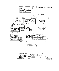
~igure 2 is a functional block d;agram of an embodiment
of the IC card of the Present invention. ln this figure, the
user of the card, designated by the numeral 7, first
commands the transaction mode bY oPerating the keyhoard 2 of
the IC card 1. This command sets the mode iudgement sec-tion
4 1 ~ ~
~ 2
4~, which remains set until a transacl;ion is comPleted.
Subsequently, the user inPuts his Personal identifica-tion
number. The input personal identification number is -then
stored in the inPut Personal identification number memorY
41, which is constructed of an internal random access memorY
(referred to as R~M hereinafter) of the IC ~. The comparison
sectlon 43 compares l;his persorlal identification number with
a reference Personal identification number reeistered in a
reference personal identification number memory 42, which is
constructed of an internal electrically erasable
programmable read only memorY (EEPROM) of the IC ~. The
function of the comParison section 43 can be realized bY a
program stored in the intern~l read onlY memorY ~referred -to
as ROM hereinafter) of the IC ~. If the comParison of these
t~lo numbers bY the comparison section 43 finds a match, a
pulse signal "1'i is Produced from the comparison section 43,
and bY the logical Product of this output and the outPu-t
from the mode iudgement section 44, a logical '1' is set in
the Personal identification number match memorY ~5 which is
eonstrueted of an internal EEPKOM of the IC ~. At the same
time, this match of the numbers also results in the
triggering of the timer circuit 46. The function of the mode
Judgement section 44 can be realized by a Program s-tored in
the internal ROM of the IC ~. The timer circuit 4G can be
formed, for examPle, of a fixed time constarlt circuit and a
~L3C~4~S9
t)l~5~;2
swilcll;ne circuil, in wllich a car)acil;or is ra~);dlY cllarged
wllile the "~IATCII" si~nal is outPul;, and arter that the
caPacil;or is d;scharged over a ~iredetermined time. These
circuits maY be t)uilt in the [C 4~ The 'MATCII' ou tPU t of the
comparison secl;()n ~3 is fed l;o l,he dis~)lay unit as we!1.
rl~is ~rives r~el mia~sion Or dis~)laY~ on the condition of the
~>ersorlal i(~entil`icalion num~(?r mal;ch, ol the balclnce st;ored
in a balarlce mem()rY 47, whieh is lorlned in tl1e inlernal
ELl)RO~i Or l;he IC ~. Althou~rh nol; illusl;rated, when l;he
0 comPalison seclion 43 rinds a mismatch, a counter, I`ormed Or
a meln()ry, r~" countirlg -the number o~ erroneous ;nPul;s is
i ncrelnen-l;ed bY one .
'l'he out~?uts ol l;he Personal identifical;ion number mat;ch
memory 4r) an~ llle timer cilcllit ~B are ou~put thr()ugh the
connect;ors, so thal; theY can be red to a bank machine or
terlninal e(lui~)merll; 8 wh~n l,he IC card is inserl,ed in and
electrically c()llllecl;ed to l;ho t;erlnirlal equir)lllellt 8.
A transa(l,i()n enab10/(lisat)le s~cl;ion $1 Or the termin
e~ui~)menl; 8 enable~ l;rarls7.lcl;i()n orlly when the output of the
~-ers()n7l1 id~-3rl~irication number mal;cll memorY ~rO and l;he
out~)ut Or the tilner circuit ~ are both set. In other words,
it ~ermits lhe (;rans.1ctiol1 on the lo~rical ;AND' conditi()n Or
t;hese two out~)uts. The Personal identi~icati()rl number match
memory ~5 and tlle m()de ~ud~r>em(!nt section ~ are reset bY a
si~rnal 8a frolll tl~ I;enlllinal e(luiPmenl; 8 which is fed f'roln
,~, .
~ 3~59
the terminal equipment 8 through the connector, after
the completion of each transactionO
In the foregoing explanation, it was mentioned
that the operation of the timer circuit 46 is
trig~ered by the "~IATCH" signal from the comparison
section 43. However, the drawback in this mechanism
is that if the prescribed valid time duration of the
output of the timer circuit 46 is over before the
user, having set the personal identification number
match memory 45 by entering the correct personal
identification number, inserts the IC card in the
terminal equipment 8, the user has to input the
personal identification number again, this time
probably in front of the other people, e~g., in a
crowded queue, so that the personal identiEication
number may be seen by othersO In order to eliminate
this problem, lt is desirable that a secondary
comparison section 48 be provided and a seconclar~
reEerence personal identification number be
registered in the reEerence personal identi:Elcation
number memory 42 so that an i.nput secondary personal
identification number can be input and a "MATCEI"
output from the secondary comparison section 48 will
re-start the time-counting operation of the timer
circuit 46. Thus, this mechanism allows the user to
~,, .
~3~
.: ~" f,
set the personal identification number match memory
45 by enterinc~ the primary personal indentiication
number at the user's home or the like in order to
maintain the secrecy of the personal identification
number, and then re-activate the output of the timer
circuit ~6 just before making the transaction by
enterinc) a simple secondary personal identification
number, which can be, for example, even the initials
of the card owner~ Of course, the primary personal
identification number can be used as the secondary
personal identification number as well.
As has been described in detail, the
above-described embodiment of the invention provides
an IC card ~hich comprises an input means, a display
means, a power supply means, a personal
identification number match memory means Eormed o a
non-volatile memory for storincJ the input of the
correct personal identiEication number throuc~h the
input means, and a timer circuit means startincJ
countin~ operation when the correct personal
identiElcation number is input, wherein the
transaction is enabled only when both are set. The
above-described embodiment is therefore applied to
highly secured cash card systems or electronic
passbook systems.
~ 12
. ,~, ~ .
,.................. .
~3~
Although the prev~ous e~planation assumes that
the personal identification number used for
veriEication of the authorized owner is a number, in
fact, any symbols other than numbers can equally be
used as a personal identification number. The term
"personal identification number" as used in the
appended claims should therefore be construed to
include such alternatives.
Moreover~ the foregoing descriptlon relates to
a configuration in which the IC 4 employs a single
chip microcomputer, containing the CPU, the memory
and the like. However, the IC may consist of plural
chips and the CPU and
~0
13
"~ ,
Olï'5~2
t;he m( lnor y ar o bu i l l; i tl sePar a l;e cll i ~s .
Ei~ure 3 is a circuit diaer~ln of an examl)le of th~
i n ror lna t i on s l;or a~c c i r cu i t wh i ch c an b~ use(l as ~ar t Or l;he
tim(?r circuil; ~ ectiorl ~() in l~i~rure 2. The inPul terininal 51
5 is corlll( cl;ed l;o lhe ~ate Or a ~`irst l;Er 52; a ~)ower supply
I ine ~1) 57 is c onnected to the drain of the f ir st l EI 52;
and a node 5~ which is -the sourc(? of the rirst l ET 52 is
~rroun(3ed throl~ l;h~ ca~)acilor 53. Th(3 node 5~ is also
conrle(:l;(d l;o tl~e ~rale Or a sec()rld ll T 5G. The drain Or the
o SeCOlld l ET 5f) is connectec! I;o the outpul; terlninal 55 an~
i tS SOUrCe i', groun(3ed.
A resisl;or 58 is l;he load resisl()r of l;he second FET
5B an(i is connecl;e(~ bel;ween !;he source of the sec()nd EET 5
and l;he Power suPPIY 1 ine Vl)l) 57.
Tl)e l~ETs Or l;h(3 above in~()rmalion slorage circuit can
be forlntd in a selnie()nductor chi~ o~` a sinfel(3 chi~) CMOS
nicr()colnpul;er . rhe r irst and l;he second l ETs can be
i m~> l emell t~3d l)Y ~ challrle I M()S EE rs ~ The cal~ac i t;or 53 can
hav1-3 a clpaci.lrlc~ in the or~Jer Or 30~ and it carl be eil;her
int;el nall~Y inc()rl)()r(ll;(1(J inl;o l.lle ch;~ or il; carl be
ex tcrna l 1 y l)r ov i (ied . l he 1 oad res i s tor 58 can be i mP 1 elnen tedby a i~OS E 1~1 Tlle r~ower su~)P I Y VDD can be abou t 1 . 5 V i n IC
car ds us i ng a o l ar ba l; ter Y . The thr esllo 1 d vo l l;a~re of` -l;he
~`irst l~ET 52 can be a~)proximalely 1~2 V due tv the back-bias
el rect and l;he l;hl esllold v()ll;.l~r(? Or l;he secvnd I~ET 56 can
1~
3 ~ 9
~l~5~2
be aPProximal;elY 0.8 V.
When -the information storaee circuit is incorpora-ted in
the timer circuit 4G of ~igure 2, the inPut terminal 51 is
connected through a level shifter 60 to the outPut of an ~ND
gate 58 having one inPut connected to the ouPtut ~4a of the
mode iudgement section ~. The other inPut of the AND gate
58 is connected to the output of an OR gate 59 receiving the
OUtPIlts ~3a and ~8a of the comparison section 43 and the
secondary com~)arison section 48. Thus. the timer is
triggered by the logical product of the output 44a of the
made Judgement section 43a and the logical sum of the
outpu-ts 44a and ~8a of the comParison section 43 and the
secondary comparison section 48.
Figure 4 shows a timing chart showing the operation of
the information storage circuit. This diagram shows that the
voltage of the Power suPPly voltage V~D, due to its
dependence UPon the solar batterY. is about 1.5 V when the
amount of light falling on the card is suf'ficient but it
drops when the card is kept in a dark place.
A h;gh Potential Pulse is aPPlied to the inPut terminal
51. This signal can be generated. for examPle~ when the
microcomputer identifies the user by the Personal
identification number inPut through -the keYboard and the
'DePosit ~ithdrawal OK' signal is outPut. This high
Potential pulse should be greater than the sum of the power
3L3q~ 5~9
0~5B2
sup~ly voltage (1.5 V) and the threshold voltag~ of the
first MOS ~ET (1.2 V). Therefore, this Pulse should be
higher than 2.7 V and PreferablY, highér than 3 V. The level
shif-ter 60 is used to raise the level (1.5 V) oF khe output
of the AND gate 58 to the level (3 V) required for inPut to
the first FET 52.
By apPlYing a pulse larger than the sum of the power
supply voltage an:d the threshols~ of the first ~ET 52, the
first FET 52 can be switched to a PerfectlY ON state, and as
a resul-t the capacitor 53 can be charged up to -the voltage
of the power SUpP~IY VDD. The voltage at the node 54 also
rises uP to the Power suPPly~voltage VDD due to the ON sta-te
of the first ~ET 52. When the voltaee at the node 54 exceeds
the threshold voltage of the second FET 5G, the second ~ET
5B also switches ON, and the voltage a-t the OlltPUt terminal
55 of the circuit becomes LOW. When -the high voltage pulse
at the inPut -terminal disaPPears, the firs-t ~I~T 52 turns
nF~, and the capacitor 53 is isolate~l from -~he Power suPPIY
Vl)D. llowever, irrespective of whel;her l;his ca~acil;or is
incorporated internallY into the I~ card or connected
ext;ernallY, a small leakaee current exis-ts betweën each
electrode of -the caPacitor and the circuit; board. The
leakage resistance is Or the order of ~o10 to 10l1 ohms.
Moreover, there~is:~leakaee curren-t throueh the FETs as
2s well, but th-is is very small~comPared to the leakage current
~ ~ IB
,
.
i 3
0~56
I.hrou~h the caPacitor. Thus, the main source Or the
discharee current in this circuit is the leakage current
l;hrough the cclPacit;or. ThereIore, ~he caPacitor 53 is
discharged ma;nlY due to its own extremelY small leakage
current. ~s a result, -lhe voltage at lhe node 54 drops
gradually. Tlle time during which the voltage at the node 54
reduces to aboul; half de~)ends upon the time constant which
is determined bY the leakage resistance and the caPacitance
of the ca~)aci-tor 53 as follows.
T = 1011 (ohm) x 30 (p~) = 50 (minutes)
Durirlg this time interval, the second ~ET 5~ is irl jan ON state
and the voltage at the outPut termiral 55 remains at the LOW
level. Moreover, during this time interval, the voltage at
the node 54 is completely isolated froln -the Power suPPlY
voltage VDD- Iherefore, the voltage at the outPut terminal
55 remains at the LOW level even in case of disaPPearance of
~he power SLI~ ,y VO Ita~e VDD as sh()wn in ~igure ~.
The LOW level state at the outPut terminal G5 can be
used as a condil,ion -~or 'De~)osit Withdrawal OK'~ l)uring the
time intervaI, ;n which ttle out~)u-t terlninal 55 is kePt LOW,
the card can be inserted in a bank terminal to withdraw cash
from the desPosit. Since the outPut signal automaticallY is
deactivated after the time interval 'T' mentioned above, it
is unlikely ttlat the card be used bY an unauthorized Person
in case of loss or the like.
~3(~4~S~
0~5B2
The above mentioned -time interval 'T' is not very
accurate since it depends uPon the leakage current of the
capacitor. Ilowever. an insulation resis-tance of the order ~-f
lO10 to 1011 ohms can be achieved without difficulty for a
30p~ externally connected caPacitor, givin~ a time interval
o~ 30 minutes t;o one hour required for making transactions
bY using the card, during which the output signal remains
LnW.
The LOW level output at the terminal 55 should
0 PreferablY be used in combination with the llICl-l level outPut
of another circui-t, e.g.l the Personal iden-tifica-tion number
match memorY 45 in Figure 2. That is -the logical Product
(AND) of the LOW level (signi~ying logical "1") of the
output 45a should be used as a condition for Permitting -the
transaction. This will Prevent erroneous operation which may
occur if the solar bat~ery breaks down or ~isconnec-tion
occurs. An alternative is to obtain the logical Product of
~he ~)ower su~Ply vol~aee VDD and the outPu~ ("1"
signi~ies "Low"j of the terminal 55. The AND gate for
such purPoses can be built in either in the external telninal
equipment, as in Pigure 2. or in the IC card itself.
As has been described, the inforlna-tion storage circui-t
employs a simPle circuit configuration but it keePs the
stored information in~tact even if the power supply voltage
disappears or drops. Therefore, when emPloyed in IC cards
18
.. ~ !
~3[)~
()1;5~j~
usine a sol(lr bat; l(!l'y, i;he abov(?-(3escr i be(J circllil; k~e~s the
output information even ir the l)OWer SUPPIy volta~e
isapr)ears due i;o inc;urricierlt; alnollnt of` I iellt ral I irlg orl
tlle solar balterY. Ilor(?over~ since the inl`()rmal ion at the
5 OU tPU t l;er m i na I au toma i; i ca I I Y i s (3eac t i va te(3 a f t et a f i xe(3
time interval, t;he ('ir('llii; al',() enSUl'(?S tli(! S(?(`Ur'il"Y ()f` i;h(?
1(, car~l.
The c i rcu i t Or the above-d(?scr~ i becl elnb()d i merl 1 carl
achieve fixe(3 i;ime intervals o~ 0 minutes l;o one hour which
10 iS relat;ivelY l()rlP, an(3 iS suilable f()r` UX(? ill 1(, (`ar(~S.
1 ()