Note: Descriptions are shown in the official language in which they were submitted.
~ 3~ 6~
66~22-47
The subject matter of this applic~tion is rela~ed to
that of Canadian Patent No. 1,28~,228 ~or "Byte Write Error
Code Method and Apparatus".
BAC~GROUND OF THE INVENTION
The present invention relates to the field of testing
of memory for a digital computer. In particular, this
invention relate~ to a pseudo-random memory test.
There ~re a nu~ber of known schemes for testing
computer memories. One prior art method is to write all binary
ones or zeros into a memory and then to read from the memory,
checking for errors. One problem with tha~ prior art method is
its inability to detect whekher two or more data lines are
shorted kogether.
Another prior art method is to remain at each memory
address long enough to write and read a series of data words at
that address, wherein each data word ~omprises zeros and a
single one~ and the data worcts dif~er in the position of that
sinyle one bit. The one bit "walks" through each bit po~ition
as the data words are wrltten into and read irom the memory.
One shortcom.tng of tha~ prior art ~qthocl is that it cannot
detect whether or nok two or more addres~s lines are shorted
together, and other prior art testing systems that write the
same data into different addresses share the inability ~o
detect whe~her or not two or more address lines are shorted
together.
Some prior art memory testers use a simple increment
by one coun~er to generate memory addresses. Some prior art
memory testers employ more than one address counter. One
4~E;4 66822-47
problem with some prior ar-t testers using coun-ter~ i5 that some
address bits generated by -the counter or counters remain the
same for relatively long periods oE time before changing s-tate.
One prior art me-thod of m~mory testing known as the
Galpat test involves staying at one address while changing data
patterns that are written into and read from that address, and
then moving on-to and doing the same at other addresses. The
amount of time it takes to run a Galpa-t test on a memory is
generally proportional to the square of the number of memory
addresses tested. Therefore, the amount of time it takes to
run a Galpat test increases dramatically for larger memories
with significantly more memory addresses.
One prior art way to check data for errors is to use
comparators to check the data read from the memory a~ainst the
data that was written into the memory. The addition of many
comparators for -testing to an existing circui-t design can,
however, take up otherwise valuable space on a printed circuit
board or within an integrated circuit.
Another prior art way to check data for errors is to
check parity. Various prior art error detecting and correcting
codes can be employed, including the Hamming code. The Hamming
code offers the ability to detect errors involving two bits and
detect and correct errors lnvolving a single bit.
S~MMARY ~ND OBJECTS OF THE INVENTION
In view of the above background, one of the objects
oE the present invention is to assure memory address uniqueness
by way of memory testing. A further related object of this
invention is to assure the independence of the address lines in
the memory~ In other words, an object oE this invention is to
, .
'I
1 provide an indication during testing of wheth2r or not two or
2 more memory addr2ss lines are shorted together or shorted to
3 any data line.
4 Another object of this invention is to assure by way
s of memory testing the independence of the data line~ in the
6 memory. An object of this invention is therefore to provide an
7 li indication during testin~ of whether or not two or more memory
8 data lines are shorted together or shorted to any address line.
9 A further ob~ect of this invention is~ to ~tor~ both a
lQ one and a zero in each location in the memory in order to
11 provide more complete testing.
12 Another object of the present invention is to better
13 simulate the randomness of real memory use by providing for
14 pseudo-random addressing of the memory and the ~toring oE ,l
pseudo-random data. A furth~r object of thi~ invention is ~,o
16 provide a m~rch through memory addresses arld data. Anoth~r
17 object of the present lnvention is to stimulate failure mode~
18 not discov~red by more regular sequences.
19 ~ Another object o~ this invention is to execute a
memory test in a relatively short time -- for example, in
21 seconds, rather ~han minutes.
22 A further object of the present invention is to add a
23 minimum of additlonal design complexity, including minimizing
24 the gate count, when memory testing circuitry is added to a
memo~y system design.
26 ll Another object of the presen~ inven~lo~ is ~o us2, in
27 1. the testing of the memory, many of the non test mode memory
28 circuitry functions. h rel~ed object of the pre~ent invention
29 ' is to use as part of the memory te~ter a portion of the non~
30 1! test mode memory circuitry.
I .
~3~ 4 66~ 47
A Eurther object of the present inven-tion is to
lmprove -the memory test coverage of the error detec-tion and
correction logic.
These and o-ther objects of the invention are provided
for by a method for testing a memory involving wri-ting a
pattern of data into the memory in a pseudo-random address
sequence determined by an address generator~ The first pattern
is read from the memory and checked for any error. A second
pattern that is the complement of the first pattern is written
into the memory in the pseudo-random address sequence determin-
ed by the address generator. The second pattern is read from
memory and checked for any error. A third pattern of data is
written into the memory in the pseudo-random address sequence
determined by the address generator. The third pattern of data
has the effect of complementing -those check bits which had
remained the same (i.e., uncomplemented) when the Eirst pattern
of data was complemented to generate the second pattern of
data. The third pattern is read Erom memor~ and checked Eor
any error.
In accordance with the present invention, an appara-
tus for testing a memory includes means for writing a first
pattern of data into the memory in a pseudo-random address
sequence determined by an address generator. Means for reading
that first pattern from the memory and means for checking that
pattern for any error are also provided. Means for writing a
second pattern o data into the memory in the pseudo-random
address sequence determined by the address generator are also
included, wherein the second pattern of data is the complement
of the first pattern. Means for reading that second pattern of
data from the memory and means for checking
-- 4 --
~.~
~ 3~ 4
1 that pattern for any error are a}so provided. Means for
2 writin~ a third pattern of data into the memory in the pseudo~
3 random address sequence determined by the address ~enerator are
4 also included, wherein the third pattern has the effect of
complel.enting those check bits which had remained the same when
6 the first pattern was complemented to generate th~ second
7 ' pattern. Means for reading the third pattern from the memory
B and means for checking that pattern for any error are also
9 provided.
Additional objects and features of the invention will
11 appear ~rom the following d~scription in which the preferred
12 embodiments have been set ~orth in detail in connection with
13 the accompanying drawings.
14
BRIE~ DESCRI-PTION OF THE DRAWINGS
16 The present invention i5 illustra~ed by way of
17 example and not limitation in the figures o the accompanyîng
lB drawings, in which like re~erences indicate similar elements,
19 and in which:
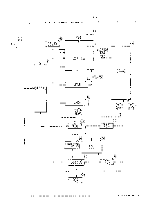
Fig. 1 is a block diagram o an embodiment for memory
21 testing;
22 Fig. 2 illustrates the data linear feedback shift
23 register;
24 Fig. 3 illustrates the address linear ~eedback shift
register;
26 , Fig. 4 illustrate~ a partial se~uence of memory
27 addresses generated by the address linear feedback shift
28 1I register;
29 !I Flg. ~ trates a me~od for testing a memory;
Pig. ~ i11ustrates part al sequences oE memory
,'.
addresses and data generated by the address linear feedback
2 shift register and the data line~r feedback shift register;
3 Fig. 7 illustrates error correction code circuitry;
~ , and
I ~ig. 8 illustrates an error correction code.
7 DETAILED ~ESCRIPTION
8 !~ With reference to the drawings, Fig. 1 illustrates in
9 block diags~m form the basic apparatus for testing the memory.
The bus 10 provides a path for data to be transferred
11 throughout many parts of a computer system. Memory system 11
12 connects with bus 10 throug~ the drivers 12, and data can flow
13 to or from bus 10 through drivers 12. Control 14 contalns,
14 among other things, circuitry to interface to and observe the li
protocol of bus 10. Control 1~ also contains circuitry to
16 control the operation of the dynamic random access memori~s
17 ("DRAMS") 16. ThiS includes control 14 providing signal~
18 including address, row address strobe ~"RAS"), and column
19 addresQ s~robe ("CAS"). Alternatively, other types of random
acces~ memories could be used in place of the DR~MS.
21 In one embodiment of the present invention memory
22 system 11 can be a memory board ~or use in a data proces~ing
23 system. In another embodiment of the present invention, the
24 memory system 1~ or use in a data processing system has at
least one memory board.
26 'I Data to be written ~rom the bus 10 into memory passe~
27 from bus 10, through the drivers 12, through data path 18, and
28 11 into DRA~S 16. Da~a to be rea~ from ~he memory onto the bus 10
29 passes fro~ D~AMS 16, through data path 1~, through drive~s 12,
! and onto bus 10.
1 Data path 18 contains error detection and correc~ion
2 circuitry for the data. Register 20 stores data read from and
3 to be written into DRAMS 16. Register 22 stores data that is
4 received from and to be sent to drivers 12. Register 28 ~tore~ ¦
S parity check bits read from and to be written into DRA~ 16.
6 . Error correction code ("ECC") circuitry 24 provide~
7 i the capabi~ity for generating check bits for data words and for
8 pro~iding sets of syndromes for data words. The operation of 'i
9 ECC circuitry 24 will be described in more detail below.
: Decode 30 contains circuitry ~o decode the syndrome
11 produced by ECC circuitry 24. If the syndrome decoded by
12 decode 30 indicates the presence and location of a correotable
13 error in the data, then corrector 26 corrects the bit of the
14 data that is in error. For example, i~ a bit should be a 1
rather than a 0, corrector 26 changes the bit from a 0 to a lq
16 Corrector 26 can of course also chan~e a 0 to a 1.
17 I decode circuitry 30 detects either a correctable
18 or an uncorrectable error, the syndrome associated wi~h that
19 error is stored in register 46. Alternatively, only if decode
l'
30 detects an uncorrectable error is the syndrome associated
21 with that error stored in register 46. Upon the detection of
2~ either a correctable error or an uncorrectable error by decode
23 30, decode 30 sends a signal to control 14, and control 14,
~4 after receiving that signal, stores in register 44 the memory
address at which the error occurred. Alternatively, deeode 30
~6 sends a slgnal to control 14 or control 14 to ~tore in
~7 register 44 the address at which an error occurred only i
28 ., decode 30 detects an ~ncorrectable error.
~9 jl Fig. ~ ~15O illus~ra~es a linear ~eedback shift
I register ("LFSRt') 40 that generates a pseudo~random sequenc~ of
!
~ -7-
g,3~ 4
1 memory addresses. The pseudo-random address ~equence simula~e~
2 the rando~ness of real memory use and may stimulate failure
3 modes not discovered by more regul~r sequences. L~SR 40
4 provides a pseudo-random address sequence for seque~cing
throu~h the memory addresses in a march. Control 14 controls
6 the enablement, disablement, and clearing of LFSR 40. The
7 ll addresses generated by LFSR 40 are provided to control 14 for
8 addressing the DRAMS 16r
9 Linear feedback shift register ("L~SR`') 42 shown in
1~ Fig. 1 generates a pseudo-random sequence of data words to be
11 written into the memory. The pseudo-random data sequence
12 simulates the randomness of real memory use and may stimulate
13 failure modes not discovered by more regular sequences. LFSR
14 42 provides a pseudo-random data sequence for generatlng a
pattern of data. Control 14 controls ~he enablement and
16 disablement o~ LFSR 42. The data ou~put o T.~S~ 42 is input
17 into register 22 of data pa~h 18. After a data word generated
1~ by LFSR 42 i~ ~tored in register 22, check bi~ for the data
19 word are then generated by ECC 74 and those check bit~ are
stored in register 28. The data word in register 22 i5 then
21 inputted into register 20. The data word stored in register 20
~2 along with the check bits stored in register 28 ~re then input
23 into DRAMS 16.
24 Delay circuitry 32 helps to avoid a lar~e power
~5 transient during start-up of a ~emory test by providing a
26 1l varlable delay to the initial start of th~ memory self test
27 l depending on the module position in the backplane~ In one
28 ll embodiment of the present inven~ion~ delay circuitry 3Z
~9 ~ncludes a c~u~e~ t~ provide a col~nt f~r the wait to start a
3~ ! memory test. The ~ounter~s count depend~ on which node ~he
~3~ 66~2~
counter is at initially, which has the effect of ,stayyering the
initiation of memory tests which in turn helps to avoid voltage
transien-ts.
Fig. 2 illustrates t~le LFSR 42 of Fig. 1. Again,
LFSR 42 generates a pseudo-random sequence of data, Fach data
word often consists of mixture of one's and zeros. LFSR 42
shown in Fig. 2 is for a 54 bit data word. A data LFSR could
alternatively be provided for generating a data word with Eewer
than 64 bits or a data word with more than 64 bits. LFSR 42
comprises 64 flip-flops and logic circuitry. The output Q of
flip-flop 54 is data bit 63, the output Q of flip-flop 56 is
data bit 62, and so forth. The output Q of flip-flop 54 pro-
vides the input D for flip-flop 56, the output Q of flip-flop
56 provides the input D for flip-flop 58, and so forth. Each
of the 64 flip-flops is clocked by a clock input provided by
control 14 of Fig. 1. The output of a logic circuit 70 that
includes exclusive-OR gates 50 and 52 is connected to inpu-t D
of flip-flop 54. Data bits Q, 1, and 2 provide an input to
logic circuit 70. Logic circuit 70 provides feedback for driv-
ing LFSR 42, and thus logic circuit 70 determines the part-icu-
lar pseudo-random data sequence for LFSR 42. The particular
LFSR 42 shown in Fig. 2 can generate approximately 109 combina-
tions of data bits. A data LFSR could alternatively be provid~
ed with different feedback logic circuitry for generating
different combinations of data bits.
Fig. 3 illustrates LFSR 40 of Fig. 1. Again, LFSR 40
generates a pseudo-random sequence of addresses which permit a
march through the memory addresses. LFSR 40 shown in Fig. 3 is
for a memory having a 25 bit address or 25 address lines. An
address LFSR couId alternatively be provided for generating
g _
. l ~
1 addresses with fewer than 25 bits ar addresses with more than
2 25 bits. LFSR 40 comprises 25 flip-flops and logic circuitry.
3 The output Q of flip-flop 90 is address bit Z4, the output ~ of
4 flip-flop 92 is address bit 23, and so forth. The output Q o
flip-flop 90 provides the input D for flip-flop 92, and so
6 forth. Each of the 25 flip-flops is clocked by a clock input
7 I provided by control 14 of Fig. 1. The output of a logic
8 circuit 106 that includes exclusive-or gates B0, 82, 84, and
9 86, and gat 88, is connected to input D of flip-flop 9U. The
Q ~Q-Not or Q-Bar) outputs o the 25 flip-flops are inputs to
11 AND gate 88. Address bits 0 through 4 are also input into
lZ logic circuit 106. Ls~ic circuit 106 provides feedback for
13 driving LFSR 40~ and thus logic circuit 40 determines the
14 particular pseudo-random address seguence for LFS~ 40. Logic
circuit 106 also permits LFSR 40 to be~in wi~h an address
16 consisting of all zeros, and nevertheless march through other
17 addresses. The all~zero address state can be ach.ieved by
18 providing the ~LEA~ inpu~ signal to all 25 flip-~lops~ Logic
19 circuit 106 also permits LFSR 40 to march through the all-zero
addres~. It should be noted that it is not necessary that data
21 LFSR 42 generate the all-zero data word given that many other
22' combinations o data bits are generated. The all-zero address
23 generated by ~SR 40,~however, permits that address to be
24 accessed during a memory test.
Fig. 4 illustrates a portlon of a pseudo--random
26 , address sequence generated by LFSR 40, including the all-zero
27 , addres~.
28 il Fig~ S illustrates the sequence for a memory te~t an~
29 1~ Fig. 1 illustra~es the apparatus employedO At step 180, a
first patt~rn of data ;s written into D~AMs 16 in accordance
--10~
1 , with a pseudo-random address sequence determined by LFS~ 40.
2 For each address generated by LFS~ 40, data LFSR 42 generates a ,'
3 pseudo-random data word, which is stored in register 22. ECC
4 : circuitry 24 generates a set of check bits for the data word,
and the check blts are stored in register 28. The data word is
6 moved to and stored in register 20, and then both the data word
7 111 in register 20 (generate~ by ~FSR 42) and its check bits in
8, register 28 ~re written into DRAMs 16. Address LFSR 40 then
9 changes to another pseudo-random address, and data ~FSR changes
to another pseudo-random data word~ and the process of writing
11 the data word and its check bits into DRAMs 16 is likewise ,
12 repeated. Fig. 6 illustrate,s a portion of the pseudo-random 'i
13 address sequences generated by L~SR 40 and a portivn of the
14 pseudo-random data words generated by LFSR 42.
E~eturning to Figs. 5 and 1, as discussed abo~e, a
16 data word is written at a memory addre~s, the next data word in
17 the pseudo-random data sequence is written at the next addres~
18 in the pseudo-random address sequence, and so forth, such that
19 a first pattern of data comprising data words is written
throughout the DR~Ms 16
21 ,. At step 184, each data word and its check bits are in
22 turn read from DRAMs 16 according to a pseudo-random address
I
23 sequence determined ~y LFSR 40. The data word read from DR~Ms
24 ~6 is stored ln register 28. At step 188, the data word and
lits check bits are checked for any error. ECC circuitry 24
26 :provides a syndrome for the data word and check bits read from
27 llthe DRAMs 16. Decode circuitry 30 then decodes the syndrome
28 111 produced by ECC cis~uitry 24. If the synd~ome decoded by
29 decode 30 indicates the presence and location of a correctable
error in the data, then correc~or 26 correc~ the bit of the
1 data that is in error.
2 If decode 30 detects either a correctable or an
3 uncorrectable error, the syndrome associated with that error is
4 stored in register 46. (Alternatively, only i decode 30
detects an uncorrectable error is the syndrome associated with
6 that error stored in register 46.) Upon the detection o~
7 1 either a correctable error or an un~orrectable error by decode
8 30, decode 30 sends a signal to control 14, and control 14,
9 after receiving that signal, stores in register 44 the memory
address at which the error occurred. (Alternatively, decode 30
11 sends a signal to control 14 for cont~ol 14 to store in
12 register 44 the address at which an error occurred only if
13 decode 30 detects an uncorrectable error.)
i4 The data word just read is then complemented by
changing all the zero bits to ones and vice-versa. Check bit~
16 for the complemented data word are then generated in data path
17 lB in the manner described above. The complemented data word
lB and its check bits are then written into D~AMs. The process o
19 reading, checking, correcting ~in some cases), and
complementing the data word is repeated for each data word in
21 the march through the memory addresses, the sequence of the
22 march through the addresses being determined by the pseudo-
23 random address sequence of LFSR 40. In that way, a second
24 pattern of data (comprising data words3 -- the complement of
the firsS pattern -- is written throughout DR~Ms 16, in
26 l accordance with step 192.
2~ .... JIl. At s~ep 196, each data word and its check bits are
28 '' read frorn DRAMs 16 according to the pseudo-random addres~
~9 1! se~uence deter~ined by LFSR 4G in the manner described above in
1l connection with step 184.
1! 12-
~3~ 66~2~-~7
At step 200, the data word read from the DRAMs and
its check bits are checked Eor the presence o-E an error in the
manner described above in connec-tion with step l88.
At step 204, a -third data pattern (comprising data
words) is written throug~lout the memory. To wri-te the third
pa-ttern of data words, certain bits of the data word read at
step 196 are complemented such that, for 64 bit data words, the
third pattern of aata is the same as the Eirst pattern of data
except for the fact that in the third pattern of data, bits 40
and 5S of each data word are complemented from what they were
in the first pattern of data. This has the effect of comple
menting those check bits that had remained the same (i.e.,
uncomplemented) when the first pattern of data was complemented
to generate the second pattern of data. Check bits are genera-
ted for the resulting new data word, and each new data word and
its check bits are written into DRAMS 16, resulting in a third
pattern of data being written throughout the memory.
At step 204, each data word and its check bits are
read from DRAMs 16 according to the pseudo-random address se-
quence determinecl by LFSR 40 in the manner described above inconnection wit~l step 184.
At step 208, the data word read from the DRAMs and
its check bits are checked for the presence of an error in the
manner described above in connection with step 188.
In one embodiment of the present invention, a correc-
table error detected during memory testing will be flagged and
the address and syndrome information will be latched for later
retrieval. A subsequent correctable error will not be flagged.
The address of the first correctable
v~
~4~6~ 1
1 error will stay latched. If only a correctable error is found
2 in the memory array, the memory will pass the self-test. An
3 uncorrectable error wi~l be flagge~ over any correctable erro-rO
4 The address and syndrome information will be latched in the
normal manner and the self-test will have failed. Any
6 subsequent correctable or uncorrectable error will not be
7 l, flagged or latched. If another uncorrect~ble error is detected
8 before the first one is cleared, a multi-error indication will
9 be set.
Fig. 7 illustrates the ECC circuitry 24. The data
11 word stored in register 20 is inputted into the decode
12 circuitry 160 of the ECC circuitry 24 shown in Fig~ 7. The
13 encode circuitry 112 generates 8 parity check bits or the data
14 word from register 20 by perorming an exclusive-OR logical
~5 operation (o~ its logical equivalent~ between certain selected
16 bits o~ the data word.
17 The generation of check bits in ~he encocle circuitry
18 160 is done according to the error correcting code ~"ECC'~) 70
lg of Fig. 8. ECC 70 is a modified Hamming Code. Each check bit
~ of the set of check bit~ is generated by an exclusive-OR
21 ("XORI') opera~tion between certain data word bits determined ~y
22 ECC 70. By reference to ECC 70 of Fig. 3, one can see which
23 data word bits determine which ch ck bits. Each check bit has~
24 its own column in ECC 70. Each "one" in the column for the
check bit of interest lines up with a bi~ position of a d~ta
26 1 word.' The data word bit positions so associated with the
2~ j "ones" in the column of interest become ~he per~inent bi~
28 ! position~. For example, for check bit S2v the pertinent data
29 1; word bit positions are 4-7, 12-~3~ 20-23, 2~-29, 36-39, 44~46,
3a 52-55, and 60-62. ~ r~eck bit is generated by ~n exclu~ive-OR
?
14-
~3~L~
1 operation between the data in the pertinent bit posi~ions of
2 the data word. For this example, check bit S2 is generated by
3 an exclusive-OR operation between the data in bit positions 4-
4 . 7, 12-23, 20-23, 28-29, 36-39, 44-46, 52-55, and 60 62 of a
data word. The 8 check bits resulting from the generation of
6 check bits in the encode circuitry 160 are stored in register
7 I' 162.
8 The 8 check bits stored in register 28 that were read
9 from memory are then inputted through gate 166 into exclusive-
OR circuitry 164. Exclusive-O~ circuitry 164 generates a
~1 syndrome by performing an exclusive-OR logical operation
12 between corresponding bit~ of each set of check bits inputted
13 into the exclusive-OR circuitry 164,
14 The syndrome generated by exclusive-OR circuitry 164
lS is then inputted into decode 30 o~ Fig. 1. The decode
16 circuitry 30 performs logical operations on the syndrome to
17 determine:
18 ~1) whether there is no error in the data word stored
19 in register 20 or the check bits stored in regist~r 28;
~2) whether the data and check bits stored in
21 registers 20 and 28 have a correctable error, and i so, the
2~ location within that data of the bit in error;
23 (3) whether the data words and check bits stored in
~4 registeIs ~ a~d 28 ~ave an uncorrectable error; and
~5 (4~ whether a failed partial write operat;on has
26 1! OCcurred.
27 ll The assumption is made, however, given the power of
28 1l ECC 7~ of ~79. 8, that there are no errors lnvolvi~ ;ee or
~9 more bits ~ the data word 7 '
l For a "write to memory" opera~ion~ the check bits of
l register 162 pass through gate 166 and are stored in register
2 ~8.
3 In an alternative embodiment of the pres2nt
4 invention, a comparator rather than error correcting code
' circuitry is used to check data for errors. In a memory te~ter
6 employing a comparator rather than error correcting code
7 ll circuitry in memory testing~ for each pattern of data in the
8 memory, the comparator detects whether or not there i5 any
9 error in the data read from the memory.
In the foregoing specification~ the invention has
ll been described with reference to specific exemplary embodiments
12 thereof. It will, however, be evident that various modifi-
13 cations and changes may be made thereto without departing from
14 the broader spirit and scope of the invention a~ set forth in
the appended claims. The specification and drawings are,
16 accordingly, to be regarded in an illustrative rather than a
}7 restrictive sense.
18
19 .,
! ;
21
2;~!
~!3
;~4
27
28 1'
29
i
-16-