Note: Descriptions are shown in the official language in which they were submitted.
~ ~3~35
Electric switching device
TECHNICAL FIELD
The present invention relates to an electric switching device
of the kind comprising a contact device with at least two co-
operating contacts, at least one of which being movable between
a closed and an open position, connection members for connec-
ting the switching device into a circuit, and two runner rails
which are each connected to a respective one of the two contacts,
said runner rails being arranged such that the arc that is crea-
ted upon contact opening, when current flows in the circuit,
under the influence of the magnetic field generated by the
current, is moved away from the contact device with the foot
points of the arc running along the rails. The switching device
may, for example, be a current limiting circuit breaker or a
current limiter arranged in series with a circuit breaker, for
example of the kind described in U.S. Patent No. 4,714,974.
BACKGROUND ART
In current limiting switching devices of the above-mentioned
kind, it is desirable that the arc leaves the contact material
as quickly as possible and travels out on runner rails 7 which
may, for example, be diverging to achieve a high arcing voltage~
or which are adapted to-insert a resistance into the circuit
in order to limit the current.
In prior art switching devices operating in accordance with the
above-mentioned principle, the arc commutation from the contacts
to the runner rails has not taken place until a relatively large
contact distance has been achieved and a relatively great amount
of ionized gas has been formed at the front end of the runner
rails. This deteriorates the current limiting ability of these
devices.
~ ~ 30 In circult breakers with separate main and break contacts it
,.. ~,. - :
-
.
304435
is known to arrange the movable break contact on a runner rail,
which in turn is movably arranged in relation to the movable
main contact (see e.g. German patent publication No. 1 272 423).
In such a circuit breaker~ a certain amount of time is required~
on the one hand, for the current commutation from the main to
the break contacts and~ on the other hand~ for the above-mentioned
arc commutation from the break contacts to the runner rails.
SUMMARY OF THE INVENTION
The present invention aims to provide, in a switching device
of the above_mentioned kind, a fast arc commutation from the
contacts to the runner rails at the initial stage oP a breaking
operation, when the contact distance is relatively small. This
is achieved according to the invention by designing the switch-
ing device so that the runner rail connected to the movable con-
tact consists of or is connected to a movable commutating con-
ductor which is so arranged that~ during the initial stage of
the contact opening~ it is at least approximately stationary
and then moves together with the movable contact to the open
position.
By arranging a movable commutating conductor, which is practi-
cally stationary during the initial stage of thR contact ope-
ning but which then moves together with the movable contact to
the open position, a more rapid arc commutation is attained
since a smaller volume needs to be ionized between the commu-
tating conductor and the opposite runner rail. This resultsin reduced cantact wear and in a faster voltage increase
across the arc.
Suitable further improvements of the invention, and the parti-
cular advantages thereof, are clear from the subclaims and the
embodiments described below.
BRIEF DESCRIPTION OF THE DRAWINGS
The invention will be described in greater detail with reference
~,:
., .
'' ~.
304435
to a number of embodiments shown in the accompanying drawing,
wherein
Figure 1 shows a schematic side view of a prior art con-
tact device~
5 Figure 2 shows in similar manner a contact device for
a first embodiment of a circuit breaker con-
structed according to the invention,
Figures 3a-3c show a contact device for a second embodiment
of a circuit breaker, constructed according
to the invention, in the closed position (Fig.
3a), at the initial stage of an opening opera_
tion (Fig, 3b), and in the open position (Fig.
3c),
Figures 4a and 4b show a section along the line IV-IV in Fig,
3b according to a first and a second alter-
native, respectively,
: Figure 5 shows a contact device for a third embodiment
of a circuit breaker constructed according
to the invention, in the open position, and
: ~20 Figure 6 shows a section along the line VI-VI in Fig,
: 5,
DESCRIPTION OF THE PREFERRED EMBODIMENTS
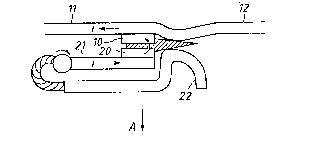
The prior art contact device shown in Figure 1 comprises a fixed
: ~ contact 10 secured to a fixed contact carrier.11, which.contact
cooperates with a movable contact 20 secured to a movable contact
:
carrier 21:, The fixed contact carrier 11 is connected to a fixed
~runner rail 12 and the movable contact carrier 21 is connected
~ :to a movabIe runner rail 22., The arrows designated i show~the
~ current direction through the contact device at a certain moment.
: : ~ :
.
' ~:
:
1304~35
The movable contact 20 is movable between a closed position,
in which it makes contact with the fixed contact 10, and an
open position, in which it is situated at insulating distance
from the fixed contact 10. Arrow A shows the direction of
movement of the movable contact 20 during an opening movement.
Figure 1 shows the device at the initial stage of an opening
movement, when the distance between the contacts 10, 20 is
still small and an arc is burning therebetween
A disadvantage of the embodiment shown in Figure 1 i5 that
it requires a relatively large contact distance before the
plasma rays P from the arc make contact~with the runner rails
12~ 22 and the arc commutation to these can take place. This
means that it takes a relatively long time before the arc leaves
the contact region so that the current can be limited and~
possibly, interrupted. During this time, considerable quanti-
ties of ionized gas and metal vapour will have time to form at
the contacts, which renders the movement of the arc from the
contact region still more difficult. In addition, burns on the
contacts may easily occur.
The above-mentioned drawbacks can be considerably reduced by
forming the runner rails as shown in Figure 2, where the movable
runner rail 22 is fixed at the beginning of the breaking opera_
tion and then~ after the arc commutation~ together with the
movable contact 20~ creates the necessary insulation distance.
The advanta~e of this embodiment is that the plasma rays which
arise at the initial stage can cause the current to commutate
rapidly because of the slight volume that needs to be ionized
between the runner rails. This leads to reduced contact wear
and a sharper voltage increase across the arc.
In the switching device of which Figure 3a shows a part, both
the fixed contact 10 and the movable contact 20 are connected
to fixed~ re:istive runner rails 12 and 23, respectively, of
the kind described in the above-mentioned U.S. Patent No.
4~714j974. The runner rails 12~ 23 are connected, via connec_
~ 35 tlng rail: 14 and 24~ respectively, to connection members 15
::
~'' ' ' ' '
' ' . .
" ~3~4~35
and 25, respectively, provided with apertures, for connecting
the switching device into a circuit. The connection member
15 is formed integral with the contact carrier 11 for the fixed
contact 10. The movable contact 20 is fixed to a contact carrier
21, which is rotatably journalled in the connection member 25
and electrically connected thereto by direct contact between
the axis of rotation and the bearing surface of the contact
carrier 11, where a relatively great contact force prevails in
the closed position of the switching device~ To prevent the
occurrence of burns in the bearing surfaces when the contact
force disappears in conjunction with the contact opening, a
flexible connecting conductor (not shown) is arranged between
the contact carrier 21 and the connection member 25. This con-
ductor may be relatively thin since it need only carry current
for a short period of time.
The rotatable conctact carrier 21 is connected to the runner
rail 23 via a commutating conductor 22 in the form of an elon-
gated resilient sheet. One end of the commutating conductor
22 is fixed to the contact carrier 21 by means of a joint 26.
The other end of the commutating conductor 22 is pressed by the
action of the natural spring force of the conductor against a
connection flap 27. To obtain as rapid an arc travelling as
possible at the contact opening phase, it is important that not
too great a part of the current is supplied to the arc via the
conductors 24, 22, since a current in this path would influence
the arc with a force in the wrong direction_ In view of this~
the electrical contact between the commutating c~nductor 22 and
the flap 27 should not be too good. Therefore, these elements
may possibly be separated by an insulating layer. To facilitate
the arc commutation, the commutating conductor 22 is fo~rmed with
a portion 28l located immediately in front of the contact 20
and projecting towards the connecting rail 14.
When a short-circuit occurs in the circuit into which the switch_
in~ device is connected~ the contact device 10, 20 is immedia-
tely opened by the influence of an automatically acting opera-
ting device ~not shown in the Figure)~ which rotates the contact
1304~3S
carrier 21 in a counter-clockwise direction. To be able rapidly
to limit the current, it is very important that a contact gap
of a certain minimum size (about 1 mm) is attained in the shor-
test possible time and that the arc thus created is rapidly
removed from the contact surfaces. As will be clear from Figure
3a, in the closed position of the switching device there is a
certain distance between the commutating conductor 22 and the
free end of the rotatable contact carrier 21~ In this way it
is prevented that the movable contact is slowed down by the
commutating conductor 22 during the initial stage of,the break-
ing operation to the position shown in Figure 3b. During the
first part of the breaking operation, the commutating conductor
22 is practically stationary. This facilitates the movement
of the arc from the movable contact 20 to the pro.jecting por-
tion 28 on the commutating conductor 22 by the action of themagnetic field generated by the current. Thereafter, the arc-
ing foot points move rapidly along the commutating conductor
22 and the connecting rail 14, respectively, to the resistive
runner rails 23 and 12, whereby the current, during the con-
tinued movement of the arc, is rapidly limited. During thelatter part of the opening movement, the commutat~ing conductor
22 moves together with the contact carrier 21 to the open posi-
tion shown in Figure 3c~ the free end of the conductor sliding
against the contact:flap 27.~
The commutating conductor 22 will carry a high.current for only
a very short time, so its thickness can be re,latively small
~e.g. 1 mm).
The movement of the arc from the contact surfaces can be further
facilitated by arranging, on each side of the contact device,
walls 41, 42 of such insulating material as gives off deionizing
gas under the influence of the arc, as will be clear from Fig-
ure 4a. In the example shown the walls are fixed on.the side
surfaces of the contact carrier 11 and project in ~ront of the
contact surface of the contact 10. A still fast.er arc commu-
tation can be achieved if, in addition, as shown in Fi.gure 4b,a plate 43 of a material eiving off gas is arranged in a recess
.
:
LS~L435
19, open towards the contact surface, in the fixed contact 10.
Also this plate 43 projects in front of the contact surface of
the fixed contact 10~ and the movable contact 20 is therefore
formed with a recess 29 adapted to the plate 43,
In the embodiment according to Figures 5 and 6, the connection
flap 27 shown in Figure 3a is omitted and instead the commuta-
ting conductor 22 rests against wedge-shaped plates 33 7 34 of,
for example, aluminium oxide (Al203), which form the inlet to
a narrow gap for the arc between the runner rails 12, 23. The
plates 33, 34 are arranged on the inside of walls 35, 36 of in_
sulating material.. At the orifice of the gap inlet.~ electrically
insulating spacers 37 are arranged~ with whi.ch the projecting
portion 28 of the commutating conductor 22 makes contact in the
closed position of the switching device~ thus obtaining a fixed
gap width of~ for example~ 1.5 mm between the commutating con_
ductor 22 and the connecting rail 14. The spacers 37 may be
made integral with the walls 35, 36. Because the free end of
the commutating conductor 22~ in the embodiment according to
; Figures 5 and 6, slides in under the end of the rurner rail 23,
the movement of the upper foot point of the arc from the commu_
ta~ing ccnductor 22 to the runner rail 23 is facilitated.
: