Note: Descriptions are shown in the official language in which they were submitted.
~304~l~5
Title of the Invention:
A PARALLEL-TO-SERXAL CONVERTER
Background of the Invention:
This invention relates to a parallel-to-
serial converter, and more speci~ically, to a
parallel-to-serial converter for multiplexing a
plurality of parallel input data into a serial
data.
Recently, transmission apparatus with high
speed operation has been achieved. The current
transmission rate in such an optical communication
system has reached the order of gigabit/second.
To obtain such a high speed transmission
rate, it is conventional practice to use multiplex
techniques. Since a parallel-to-serial conversion
is considered a simple method of multiplexing, a
parallel-to-serial converter is often used for a
multiplexer operated under high speed.
Moreover, it has also been known to employ a
synchronous multiplexing network, such as
Integrated Services for Digital Network ("ISDN")
and Synchronous Optical Network ("SONET"), to
easily connect the communication systems. The
basic transmission rate is selected to several
tens of megabit/second and a multiplexing pulse
!
~L3~
21.1525 - 2 - PATENT
code modulation ("PCM") hierarchy is set to an
integer multiple of this basic transmission rate.
In this synchronous multiplexing system, each
network and each transmission line are
synchroni~ed with each other in order to easily
connect one network to another and to form a
simple and less costly multiplexer by parallel-to-
serial conversion.
Therefore, a parallel to-serial converter is
now fre~uently employed for a multiplexer to
realize a stable high speed data transmission yet
less costly system.
As transmission speed has increased, however,
converting a plurality of parallel input data into
a serial data adversely reduces the phase margin
in the parallel-to serial converter, in view of a
phase relation between a clock signal deciding an
output timing of each of the parallel input data
and the parallel input data themselves.
Accordingly, in such a high speed operation, a
rising time and falling time of a waveform of an
input data, and a set up time and holding time of
circuit elements in a parallel-to-serial converter
cannot be neglected so that the phase margin of
,
21.1525 - 3 - PATENT
input data is occupied by the above rising and
falling time and the set up and holding time.
When the phase margin becomes reduced, it is
difficult to realize a stable operation and a
S higher speed operation of a parallel-to~serial
converter.
Summar~ of the Invention:
Therefore, it is an object of the present
invention to improve the phase margin oE a
parallel-to-serial converter.
It is a further object of the present
invention to realize a stable and higher speed
operative parallel-to-serial converter.
Additional objects and advantages of the
invention will be set forth in part of the
description which follows, and in part will be
obvious from the description, or may be learned b~
practice of the invention. The objects and
advantages of the invention may be realized and
obtained by means of the instrumentalities and
combination particularly pointed out in the
claims.
~3~4~
.
4 25307-212
According to a broad aspect of the invention there ls
provided a parallel-to-serial converter for multlplexing a
plurality of parallel input data into a serial data, comprislng:
(a) means for multiplying an input clock by n, wherein n is
an integer greater than or equal to 2, sald input clock being in
synchronism with one of the plurality of parallel input data and
for generating a multiple clock in synchronism with ~he serial
data;
(b) means for dividing the multiple Glock by n and
generating a plurality of divided clock signals, each of said
plurality of clock signals being in synchronism with one of the
plurality of paralle]. input data;
(c) means for converting the plurality of parallel input
data into a.serial data output in reference to a tlming of said
plurality of divided clock signals from said dividing means;
(d) means for shaping a waveform of the serial data output
from said conver~ing means using the multiple clock from said
multiplying means;
(e) means for comparing a phase relationship between the
divided clock signal and the input clock representing a phase of
one of the plurality of parallel input data; and
(f) means for adjusting a phase relationship between the
plurality of parallel input data and the plurality of divided
clock signals under the control of said comparing means.
,h~
~L3~4~
21.1525 - 5 - PATENT
rief Description_of the Drawings:
The aeeompanying drawings, which are
ineorporated in and eonstitute a part of this
speeifieation, illustrate embodiments of the
invention and, together with the description,
serve to explain the prineiples of the invention.
FIG. 1 is a eireuit diagram of the prior art
parallel to-serial eonverter;
FIG. 2 is a timing ehart illustrating signal
waveforms at respeetive points of the circuit
diagram of FIG. 1 for explaining the operation of
the prior art eonverter of FIG. l;
FIG. 3 is a bloek diagram of an embodiment of
a parallel-to-serial eonverter in accordance with
the present invention;
FIG~ 4 is a bloek diagram of another
embodiment of a parallel-to-serial eonverter in
accordance with the present invention;
FIG. 5 is a timing ehart illustrating signal
waveforms at respeetive points of the parallel-to-
serial converter of FIGS. 3 and 4;
FIG. 6 is a eircuit diagram for the parallel-
to-serial converter of FIG. 3;
.
~31[~9~5
21.1525 - 6 - PATENT
FIG. 7 is a timing chart illustrating signal
waveforms at respective points in the circuit
diagram of FIG. 6;
FIG. 8 is another circuit diagram for the
parallel-to-serial converter of FIG. 3;
FIG. 9 is a timing chart illustrating signal
waveforms at respective points of the circuit
diagram of FIG. 8;
FIG. 10 is a circuit diagram for the
parallel-to-serial converter of FIG 4; and
FIG. 11 is a timing chart illustrating signal
waveforms at respective points of the circuit
diagram of FI&. 10.
Detailed Description of the Preferred Embodiments:
lS Before describing the present invention, the
prior art parallel-to-serial converter will be
described and then the reason for and method of
improving a phase margin will be explained.
FIG. 1 is a circuit diagram of the prior art
parallel-to-serial converter. In FIG. 1, a
multiplexing circuit 13 receives a pair of input
data D1, D2 for parallel-to-serial COnversiQn and
outputs a serial multiplex data MD1. These input
~48~L5i
21.1525 7 - PATENT
data Dl, D2 are synchronizing with each other. An
input clock ~0 is also synchronizing with these
input data Dl, D2. A flip-flop circuit 15 is
provided at the output of multiplexing circuit 13
for discriminating and shaping multiplex data MD
and for outputting a multiplexed data MD2. A
multiplier 17~ connected to input clock ~0,
outputs multiple clock ~3 by multiplying two times
a frequency of the input clock ~0. A dividing
circuit 19 divides a frequency of multiple clock
~3 into 1/2 and generates a couple of divided
clocks ~1 and ~2 having reverse polarities
respectively.
The multiplexing circuit 13 has three NOR
circuits to convert the input data Dl, D2 into
serial multiplex data MDl by alternately selecting
such input data with the phase of frequency
divided clocks ~ 2 input from the dividing
circuit 19. Namely, the input data Dl, D2 are
read out one-by-one when the divided clocks ~ 2
are in the "L" or "0" level and either this read
out input data Dl or D2 is output as the multiplex
data MDl. The multiplex data MDl is then input to
the flip-flop circuit 15, discriminated "0" or
~3~ 45
21.1525 - 8 ~ PATENT
"1", and shaped therein by the multiple clock ~3
from the multiplier 17 through reformation. This
is then the output as the multiplex data MD2.
A time chart of respective signals in the
prior art parallel-to-serial converter of FIG. 1
is shown in FIG. 2. Operation of this parallel-
to-serial converter will be further ~xplained with
reference to FIG. 2.
As shown in FIG. 2, the input data D1, D2 are
mutually shifted in the phase by ~ (radian) to
keep the sequence between the two input data D1,
D2. Phase relations of the input data D1, D2 and
input clock ~0 are previously adjusted by the
phase adjusting circuit not illustrated so that
they are in a constant phase relation.
The multiplexing circuit 13 selects the
parallel input data D1, D2 in the timing of
divided clocks ~ 2 to convert these parallel
data into the series data as the time series
multiplex data MD1. Namely, the multiplexing
circuit 13 selects and outputs the input data D
when the divided clock ~1 is in the "0" or "L"
level and the input data D2 when,the divided clock
~2 is in the "0" or "L" level.
~30~5
21.1525 - 9 - PATENT
This multiplex data MD1 is discriminated "0"
or "1" and shaped by the fl.ip-flop 15 in the rise
timing of the clock ~3 and is then output as the
multiplex data MD2 in the defined phase and time
interval.
In this prior art parallel-to-serial
converter, the multiple clock ~3 output from the
multiplier 17 is divided in the dividing circuit
19 and the divided clocks ~ 2 are used as the
multiplexing clocks in the multiplexing circuit 13
in order to synchronize the divided clocks ~ 2
with the multiple clock ~3.
In the prior art parallel-to-serial converter
shown in FIG. 1, the polarity of divided clocks
~ 2 output from the dividing circuit 19 cannot
be defined because of the nature of discrimination
flip-flop 15 so that it is possible, for example,
that the converter provides the divided clocks
~ 2 having polarity inverted from divided
clockS ~ 2- Therefore, in case the read
timing defined by divided clocks ~ 2 is set to
be located at the center of input data D1, D2 on
the occasion of reading the input data D1, D2 by
the multiplexing circuit 13, if the polarity of
~481~
21.1525 - 10 - PATENT
divided clocks ~ 2 is inverted and the divided
clocks ~ 2 appears, the data is read at the
data converting point of the input data D1, D2 and
read error may be generated.
Accordingly, in the prior art parallel-to-
serial converter, the timing of reading the input
data D1, D2 with the divided clocks ~ 2 is set
to the front half or back half position of the
input data D1, D2 and thereby read error is no
longer generated if the polarity of divided clocks
2 is Converted.
However, using only the front half or back
half position of input data D1, D2 for a read out
timing substantially reduces the phase margin to a
half. With recent advancement in transmission
rates, a high transmission rate system cannot set
the rising time t(r) or falling time t(f) of the
input ~ata D1, D2 to a sufficiently higher value
relative to the transmission rate and also cannot
neglect the setup time and hold time of the
discrimination flip-flop 15. Accordingly, such a
high transmission rate system would significantly
reduce the phase margin in the prior art parallel-
to-serial converter.
~L3~AS
21.1525 - 11 - PATENT
In accordance with the invention, it has been
found that the phase margin must be improved by
conducting discrimination at the center point of
each of the input data in a parallel-to-serial
converter. Block diagrams of two preferred
embodiments of the present invention are shown in
FIG. 3 and FIG. 4.
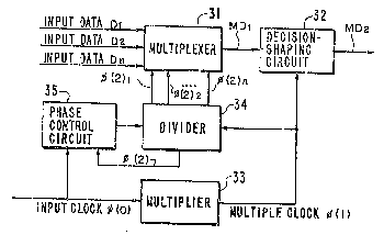
The first preferred embodiment of a parallel-
to-serial converter of the present invention is
shown in FIG. 3. A multiplier 33 generates a
clock ~(13 having N-multiple frequency of an input
clock ~(o)~ As used herein, N is an integer which
is equal to 2 or larger than 2. A dividing
circuit 34 generates N divided clocks ~(2)1 ~
~(2)n by dividing the fre~uency of multiple clock
~(1) of the multiplier 33 into 1/N. A
multiplexing circuit 31 receives in parallel the
inpu~ data D1 ~ Dn to be converted into a series
data MD1 and multiplexes input data D1 ~ Dn in
accordance with the phase of N divided clocks
~(2)1 ~ ~(2)n from the dividing circuit 34. As
previously described with reference to the
converter of FIG. 1, the input data D1 ~ D~ are
synchronizing with each other and the input clock
. ~3048~S
21.1525 - 12 - PATENT
~(0) is also synchronizing with these input data
D1 ~ Dn~ A decision and shaping circuit 32
discriminates "0" or "1" of the multiplex data MD
received by circuit 32 from the multiplexing
circuit 31 and shapes such data MD1 with multiple
clock ~(1) received from the multiplier 33.
phase control circuit 35 compares the phase of the
input clock ~(0) with that of divided clock ~(2)
of the dividing circuit 34 and controls the output
phase of divided clock ~(2) of the dividing
circuit 34 so that the divided clock ~(2)1 ~ ~(2)n
synchronizes with the input clock ~(0).
The above embodiment is based on the concept
of controlling a phase of the divided clock ~(2)1
- ~(2)n for improving a phase margin. Namely, by
controlling a phase of the divided clock ~(2)1 ~
~(2)n~ a phase relationship between the parallel
input data Dl ~ Dn and the divided clock ~(2)1 ~
~(2)n can be adjusted so that a phase of the
divided clock is positioned at the center of a
phase of the parallel input data D1 ~ Dn.
Another preferred embodiment of the parallel-
to-serial converter of the present invention is
shown in FIG. 4. A multiplier 33 generates a
~30~1 34~i
21.1525 13 - PATENT
multiple clock ~(1) from an input clock ~(0). A
dividing circuit 34 generates N divided clocks
~(2)1 ~ ~(2~n by dividing the frequency of
multi.ple clock ~(1) from the multiplier 33 into
1/N. A phase shif~ circuit 261 ~ 26n respectively
shifts phases of input data D1 ~ Dn to be
converted into d1 ~ dn by a predetermined value.
A selection circuit 27 selects either input data
D1 ~ Dn or shifted input data d1 ~ dn~ A
multiplexing circuit 31 receives in parallel the
input data D'1~ Dln from the selection circuit 27
and multiplexes D'1 ~ Dln into MD1 in accordance
with the phase of N divided clock ~(2)1 ~ ~(2ln
from the dividing circuit 34.
As was explained with reference to the
embodiment of FIG. 3, input data D1 ~ Dn and input
clock ~(0) are synchronizing with each other. A
decision and shaping circuit 32 discriminates "0"
or "1" of the multiplex data MD1 from the
multiplexing circuit 31 and shapes such multiplex
data MD1 with the multiple clock ~(1). A
selection control circui~ 28 compares the phase of
the divided clock ~(2) with that of input clock
13~45
21.~525 - 14 - PATENT
~(0) and controls a changeover operation of the
selection circuit 27.
This second preferred embodiment is based on
the concept of controlling a phase of the input
data Dl ~ Dn instead of the divided clock ~(2)1 ~
~(2)n in order to improve a phase margin. Namely,
by controlling a phase of the parallel input data
D1 ~ Dn/ a phase relationship between the parallel
input data D1 ~ Dn and the divided cloc~ ~(2)1 ~
~(2)n can be adjusted so that a phase of the
divided clock is positioned at the center of a
phase of the parallel input data D'1 ~ Dln.
A time chart of signals at respective points
for the parallel-to-serial converters of FIGS. 3
and 4 is shown in FIG. 5. With respect to the
converter of FIG . 3, phase control circuit 35
compares the phases of input clock ~(0) and
divided clock ~(2) and thereby controls the output
phase of the dividing circuit 34 so that data is
read out at the center position of the data D1 ~
Dn to be converted by the divided clocks ~l2)1 ~
~(2)n in the multiplexing circuit 31.
In the parallel-to-serial converter of FIG.
4, if the phase of data D1 ~ Dn to be converted
i30~EI4LS
21.1525 - 15 - PATENT
and the divided cloeks ~(2)1 ~ ~(2)n are mutually
deviated in the multiplexing eireuit 31, such
deviation can be deteeted by eomparing the input
eloek ~(0) and the divided eloek ~(2) ln the
seleetion eontrol eircuit 28 because the input
eloc~ ~(0) is synehronized with data D1 ~ Dn. The
ehangeover operation is earried out in the
selection circuit 27 depending on such deteetion
and thereby the ~data d1 ~ dn to be converted whieh
have been shifted a speeified amount in the phase
shifting eircuit 261 ~ 26n are supplied to the
multiplexing circuit 31. As a result, the data
read out operation is carried out at the eenter
position of data d1 ~ dn to be converted by the
divided eloeks ~(2)1 ~ ~(2)n in the multiplexing
cireuit 31 and thereby the phase margin can be
improved.
Further details and explanation of the
embodiments of FIGS. 3 and 4 will now be made with
reference to FIG~. 6 to 11.
FIG. 6 is a circuit diagram for the parallel-
to~serial converter of FIG. 3. This circuit
includes a multiplexing circuit 31, a decision-
shaping flip-flop 32, a multiplier 33, a dividing
~3~4~4LS
21.1525 - 16 - PATENT
circuit 34 and a phase comparison circuit 35. The
dividing circuit 34 includes a ~lip-flop having a
set pulse input terminal. When the set pulse is
applied to the set pulse input terminal, the
polarity of output Q (namely, the divided clock
~1) becomes "H" or "1".
Moreover, the phase comparison circuit 35
includes a NOR circuit with three inputs. The
input clock ~0, divided clock ~1 from the dividing
circuit 34 and the clock ~3' obtained by delaying
the phase of the multiple clock ~3 from the
multiplier 33 with the predetermined degree are
such three inputs to circuit 35. When the three
inputs are all "0" or "L", the set pulse ~4 is
output to the set pulse input termiAal of the
dividing circuit 34.
Operation of this embodiment is explained by
referring to FIG. 7 which is a time chart of
signals thereof at respective points of the
circuit of FIG. 6. As explained with re~erence to
FIGS 1, 3 and 4, input data Dl, D2 and input clock
~0 are synchronizing with each other. In this
embodiment, when the divided clocks ~ 2 are in
the "L" level, corresponding NOR circuits are open
,.. ,; , .. ...
1~1048A5
21.1525 - 17 - PATENT
and the input data D1, D~ are read out from a
multiplexing circuit 31 via corresponding NOR
circuits. Here, the input clock ~0 has previously
been adjusted in its phase so that the "H" level
thereof is positioned at the center of input data
D1. In this embodiment the phases of divided
clocks ~ 2 are adjusted with reference to the
phase of this clock input ~0.
Namely, the output phase of dividing circuit
34 is adjusted so that the polarities of input
clock ~0 and divided clock ~1 have inverted
polarities with each other. This polarity
inversion can be achieved by outputting the set
pulse ~4 to invert the polarities of outputs Q, Q
of the dividing circuit 34 whe.n both input clock
~0 and divided clock ~1 are in the "L" level
(refer to time t1 in FIG. 7). Thereafter~ the
input data D1, D2 are thereby read out
respectively by the divided clocks ~ 2 at the
center position of these clocks.
The clock ~3' to be input to the phase
comparison circuit 35 is used for narrowing the
comparison period so that an erroneous set pulse
is no longer output due to the existence of noise
. ~
~L3~8~5
21.1525 - 18 - PATENT
at the time of comparing the input clock ~0 with
the divided clock ~1
It can be readily seen that the present
invention allows for a variety of modifications or
changes in circuit design for the converter. For
example, FIG. 8 is another alternative circuit
diagram for the parallel-to~serial converter
embodiment of FIG. 3. In this circuit diagram,
the phase adjustment of divided clocks ~ 2 is
carried out b~ inhibiting the multiple clock ~3 to
be input to the dividing circuit 34.
The circuit of FIG. 8 includes a multiplexing
circuit 31, a flip-flop 32 as a decision and
shaping circuit, a multiplier 33, a dividing
circuit 34, a phase comparison circuit 35 1 and an
inhibit circuit 35-2. The functioning of phase
comparison circuit 35-1 and inhi~it circuit 35-2
correspond to the phase control circuit 35 of FIG.
3. The phase comparison circuit 35~1 has a NO~
circuit 39 which receives the input clock ~0 and
divided clock ~1 and a flip-flop 38 which receives
an output of the NOR circuit 39 at the data input
terminal D and the clock ~3' having a
predetermined phase dela~ of the multiple clock ~3
~3~4~345
21~1525 - 19 - PATENT
at the clock input terminal C of flip flop 38.
The output pulse ~5 of the flip-flop 38 is output
to the inhibit circuit 35-2.
The inhibit circuit 35-2 is formed by a 2-
input NOR circuit and receives the input pulse ~5
and multiple clock ~3 respectively and supplies
output clock ~6 to the dividing circuit 34.
Operation of this embodiment will be
explained hereunder with reference to FIG. 9.
FIG. 9 is a time chart of signals at respective
points of the circuit of FIG. 8. In this
embodiment, when the polarity of divided clock ~1
is inverted from the normal polarity, it is
detected (refer to the time t1 in FIG. 7) in the
phase comparison circuit 35-1 from the fact that
both input clock ~0 and divided clock ~1 are in
the "O" or "L" level at the rising edge of the
clock ~3'. Thereby the output pulse ~5 is sent to
the inhibit circuit 35 2 and one pulse of the
multiple clock ~3 inhibited by this inhibit
circuit 35-2 is extracted and then supplied to the
dividing circuit 34 as the clock ~6.
Accordingly, the polarities of divided clocks
2 output from the dividing circuit 34 are
",,.:
13~4~3~5
21.1525 - 20 - PATENT
inverted and thereafter the input data D1, D2 are
read out at the center position by the divided
clockS ~ 2~
A circuit diagram for the converter
embodiment of FIG. 4 is shown in FIG. 10. In this
circuit diagram for the converter of FIG. 4, the
phases of input data D1, D2 are shifted by
~(radian) (instead of the FIG. 3 converter where
the polarities of divided clocks ~ 2 are
inverted) when the phases of d.ivided clocks ~ 2
for reading out the input data D1, D2 are inverted
with respect to the phase of the input clock ~0,
The operation of the circuit of FIG. 10 is
now described with reference to FIG. 11. FIG. 11
is a timing chart illustrating signal waveforms at
respective points of the circuit of FIG. 10.
As described for the converter of FIG. 6 and
the respective timing chart of FIG. 7, the input
clock ~0 has previously been adjusted in its phase
so that the l'H" or "1" level thereof is positio~ed
at the center of input data D1. See FIGS. ll(a)
and (b).
This circuit of FIG. 10 includes phase delay
circuits 261, 262 for delaying input data D1, D2
~304a4s
21.1525 - 21 - PATENT
with ~ rad respectively. See FIGS. ll(b),(e~ and
(h3, and (i)). That is, the polarities of input
data Dl, D2 are inverted. A selection circuit 27
selects either one of the input data D1, D2 or
delayed data d1, d2 in accordance with selection
signals SEL1 and SEL2 from a control circuit 28.
A control circuit 2~ compares a phase of the clock
~0 with that of the divided clock ~1 and contxols
changeover operation of selection circuit 27
depending on the result of the comparison.
As mentioned previously, the input clock ~0
is adjusted so that the l'H" level thereof is
positioned at the eenter of an input data D1
(FIGS. ll(a) and (b)). This means that the phase
of the input clock ~0 coincides with the phase of
the divided elocks ~1 and ~2. However, since a
controI circuit comprises a flip-flop for
comparing the phases of the input clock ~0 and the
dlvided elocks ~1 and ~2~ this control circuit 28
cannot compare the phases if the phase of the
input eloek ~0 coineides with the phase of the
divided elocks ~1 and ~2~ due to the nature of a
flip flop. Therefore, the phases of the divided
~L3~4~5
21.1525 22 - PATENT
clock ~1 and ~2 from divided circuit 34 are
adjusted to add ~rad delay by buf~er 54 and delay
circuit 51~FIGS. 11 (a), (e) or (g)), so that a
flip-flop of control circuit 28 can compare the
phase relationship between the input clock ~0 and
a divided clock ~1~ that is, between the input
data Dl and a divided clock ~1
When the phase relationship between the input
clock ~0 and a divided clock ~1 is normal, as
shown in FIGS. ll(a), (d), (e), a selection signal
SELl, which is an output from Q terminal of
control circuit 28, is at an "L" level, and a
selection signal SEL2, which is an output from Q
terminal o~ control circuit 28, is at an "~"
level, so that a selection clrcuit 27 selects
input data Dl and D2 for outputs D'l and D'2
(FIGS. ll(b),(h)). Consequently, a multiplexer
converts parall.el input data D'l and D'2 into a
serial multiplexed data MDl as shown in FIG.
11 ( i ) -
To discriminate a multiple~ed data ~Dl at the
center thereof by a multiple clock ~3 (FIG.
ll(k)), a phase of a multiple clock is adjusted by
buffer 52 as shown in FIG. 11(1).
i~4L~3~L5
21.1525 - ~3 - PATENT
On the other hand, when the phase
relationship between the input clock ~0 and a
divided clock ~1 is in reversed condition, that
is, a polarity of a divided clock ~1 rom a
divider 34 is inversed as shown in FIG. ll(f),
selection signals SEL1 and SEL2 from control
circuit 50 turn into "H" and "L" level,
respectively. Then selection circuit 27 selects
input data d1 and d2 for outputs D'1 and D'2 (FIG.
ll(c),(i)). A multiplexer, then converts parallel
input data D'1 and D'2 into a serial multiplexed
data MD1 as shown in FIG. ll(m). A multiple clock
is delayed by buffer 52 like FIG. ll(o).
Furthermore, a buffer 53 is just a timing
interface to a next circuit and includes a flip-
flop.
The embodiments of the converter have been
described above as performing parallel-to-serial
conversion of two input data. However, the
present invention is not limited only to such
input data. For example, when there are N
parallel input data, a multiplier multipl~ing
input clock frequency by N and a dividing circuit
dividing a multiple clock frequency by 1/N can be
13041345
21.1525 - 24 - PATENT
used instead of the multiplier multiplying input
clock frequency by 2 and the dividing circuit
dividiny a multiple clock frequency by 1/N as
shown in FIGS. 3, 4, 6, 8 and 10. It will be
apparent to those skilled in the art that
modifications and variations could be made to the
parallel-to-serial coinverter in accordance with
the teachings of the invention without departing
from the spirit or scope of the invention. Thus,
it is intended that the present invention cover
the modifications and variations of the invention
within the scope of the claims and their
equivalents.