Note: Descriptions are shown in the official language in which they were submitted.
r~ I LN I -- :~U--~
~3~S~
BACKGROUND OF THE INVENTION
.__
The present invention relates to capacit~ve touch pads and
more particularly 'tQ novel touch pad construction enabling the ple3sing
appearance of light-colored touch pids for an applianse control panel.
Use of glass capacitiYe touch control pane~s for appliance
controls ls well known. However, such control panels typitally employ
touch pads which are relatively dark in ~olor. Current trends ln
kitchen design have created a need for a glass capacitance touch
control panel with white touch pads with black lettering a11d/Or
symbols. The control par,el touch pads must meet the normal standards
Ç~ ~or such panels~fti~at the pad nmst be conductive, ~st be of at
least a minimum size, and must be resistant to abrasion and to
corrosive food stuffs. Such pads are normally applied by ;creen
printing a ceramic enamel to which a metallic powder has been added.
The printed film is then fired to form a conductive glassy film. The
conventional approach providss satisfactory results for relatively
dark-colored pads. However, the necessary addition of commonly used
conductive metallic components to a white enamel darkens the enamel
resulting in an off-white or gray color. Use of almost pure silver as
the metallic component results in 2 reasonably satisfactory white
color; howe~er, it lacks other required properties and is subject to
tarnishing on exposure to the air.
In view of the aforementioned shortcomings of the pr~or art, a
reed exists for a means of providing capacitivE touch control panel
havi ng whi te touch pads .
013JECT OF THE ~NVENTION
It is therefore a primary object of the present invention to
provide a glass capacitance touch control panel for an appl~arce
featuring white tollch pads with black lettering.
_l _
~k
PATENT 9D-MA-17064 - Schultz, Jr.
~3~S~
SUMMARY ûF THE INVENTION
A capacitive touch pad Asse~ly in accordance tlrith the present
invention has a thin dielectric layer or substrate having an outer
touch electrode of a relatively dark-colored conductive material
deposited on its outer surface and a pair of spatially separated inner
electrodes for0ed on its inner surface for connecting to the control
circuitry. To achie~le a light-colored appearance for the touch pads, a
layer of relatively light-colored non-conductive decorative material ts
applied to the outer surface overlaying the touch electrode to hide its
dark color except for a small exposed area of the electrode whicll may
define a symbol relating to ehe function nf the Pad. The exposed area
provides the means for direct human body member contact with the outer
touch electrode.
Preferably the outer electrode is formed by screen printing or
otherwise depositing a screena91e paste comprising a mixture of finely
ground black glass particles~,~ a conductive metallic powder, in an
organic medium, ~hich is covered w;th a layer of non-conductive white
ceramic enamel except for the small exposed area. The exposed area
provides the black lettering or other synbol on the touch pad.
In accordance with another aspect of the invention, the layer
of decorative l~laterial may be applied in ~ultiple coats to provide
adequate coverage to hide the underlying dark electrode. Surh Inultiple
eoats if not aligned precisely may result in an unsightly uneven border
for the exposed area. To relieve the alignment ~roblem and enhance the
appearance~ a second layer of dark conductive material covers the
exposed area aad the immediately adjacent portions of the decorative
layer thereby defining a slightly enlarged version of the sy~rbol
deflned by the exposed area.
.
.'
~5~
9D-MA-17064
In accordance with yet another aspect o~ the
invention, the outer el.ctrode is formed of a gray or silver
material to facilitate one coat coverage by the decorative
layer. A layer of black conductive material covers the
exposed area and the immediately adjacent portions of the
decorative layer again defining a slightly enlarged version
of the symbol defined by the exposed area.
BRIEF DESCRIPTION OF TXE DRAWIl!~GS
While the novel features of the invention are set
forth with particularity in the appended claims, the
invention, both as to organization and content, will be
better understood and appreciated from the following
detailed description taken in conjunction with the drawings
in which:
FIGS. lA and lB are respectively top and side views
of a portion of a touch conkrol panel illustrating a pr.ior
art touch pad construction;
FIGS. 2A is a plan view of a capacitive touch
control panel for a range surface unit;
FIG. 2B is a bottom view of a portion of the
control panel of FIG. 2A showing one of the control panel
touch pads;
FIG. 3A is a plan view of the touch pad of FIG. 2B;
FIG. 3B is a sectional view of the touch pad of
FIG. 3A taken along section lines 3B-3B;
FIG. 4A is a plan view of an alternative touch pad
construction for the touch pad of FIG. 2B; and
FIG. 4B is a sectional view of a touch pad of FIG.
4A taken along section lines 4B-4B.
DETAILlE~D DESCRIPTION
Referring initially to FIGS. lA and lB, a prior art
capacitive touch pad construction designated generally 10
includes a dielectric substrate 12; a touch electrode 14 of
electrically conductive material, fabricated on the outer
facing surface 12A of substrate 12, having a preselected
boundary of generally rectangular shape; and pair of inner
'~
-3-
PATENT - 9D-MA-17064 - Schultz, Jr.
electrodes 16 and 18 commonly referred to as a transmitting electrode
and a receiving electrode respecSively, fabricated ~n the inner surface
12B of substrat~ 12 underlying and substantially ~ithin ~he boundary of
electrode 14. The transmitting and receiving electrDdes are adavted
for connection to ~e71-known electronic control circuitry /not shown
for simplicity). Such circuitry typically is configured to dri~e the
transmitting electrode with a scanning pulse and to recogni~e a change
1n the amplitude of that pulse at ~he receiving electrode as the
effective series coupling impedance bet~een transmitting and receiving
~lectrodes varies when touch electrode 14 is contacted by a human body
member.
As described in the Background discussion such prior art touch
pdd assemblies feature dark-colored touch pads because the addition of
metallic powder to the enamel which is deposited on the substrate to
form the pad electrodes inherently darkens the enamel. Thus, there are
no known conductive enamels which meet both the whiteness requ~rement
and possess the aforementioned physical and electr;cal characteristics
required for touch pads for an appllance control panel.
The present invention overcomes the aforementioned deficiences
of the prior art in accordance with the present inYentiOn by pro~iding
a capacitive touch pad assem~y for an appliance control Panel which is
relatiYely light, preferably white, in color.
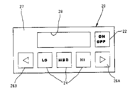
An illustrative appliance control panel 20 for a range cooktop
is shown in Fig. 2A. Control panel 20 is a capacitive touch control
panel with an ON/OFF touch pad 22, touch pads 24 for selecting low,
medium and high ~ower settings for the surface unit, and slew touch
pads 26A and 26B for slewing the power setting selection up and down
resFecSively. Pads 22~ 24 and 26A ~ H ~are formed on a dielectric
substrate 27 preferab~y of t~pered glass. Nsrmally in control panel
PATENT - 9D-MA-17064 - Schultz, Jr.
~3~
applications the inner surface of the glass is coated ~ith an opaque
decorative film prior to ~pplication of the inner electrodes. This
filw may be a ceramic enamel or an organic material. In ~he panel of
the illustrative embodiment a rectangular port;on of the glass is not
covered by ~he opaque film to provide a viewing window 28 for
underlying display elements ~hich may be vacuum ~ uorescent devices or
LEDs or other elements suitable for providing a Yisual indication of
the selected power setting for the surface unit.
In control panel 20, each of the touch pads is a relatively
light color, preferably ~hite. The triangular slew symbol on pads 26A
and 26B and the lettering on pads 22 and 24 is a relatively dark color,
preferably black.
As w~ll be described hereinafter in greater detail with
respect to pad 26B, the various function indicating sy~bols on the pads
are defined by screen printing the white enamel decorative finish over
the black electrode using a drop out lettering technique such that the
exposed area of ~he electrode defines the symbols which may be letters
or other indicia for identifying the function of the pad to the user.
Referring now to Figs. 2B~ 3A and 3B, the constructlon of slew
touch pad 2fiB will be described in greater detail. It is to be
understood that the other touch pads are similarly constructed varying
only in ~he shape of the symbol defining exposed area. Fig. 2B shows a
portion of the inner s~de of control panel 20 contdining touch Pad
26L. The inner electrodes 30 and 32 for touch pad 268 are fabricated
on the inner surface of substrate 27 underlylng and within the boundary
of outer electrode 34 in a conventional manner such as by by screen
printing a cond~ctive metallic paste on ~he glass in the desir~d
configuration. Leads 30A and 32A extend from electrodes 30 and 32
respectively for connection with external electronic control circuitry
(not shown)~
--5--
~3~S~
9D~MA-17064
FIG. 3A is a top view of touch pad 26B. FIG. 3B is
a sectional view of the portion of control panel 20 shown in
FIG. 3A taken alony lines 3B-3B, showing the electrodes 30,
32 and 34 together with the layer of re:Latively light-
colored decorative material 36 which overlays electrode 34except for an exposed area 38 which def:ines the triangular
"slew" symbol. In FIGS. 3A and 3B, the leads from
electrodes 30 and 32 are not shown for simplicity and
clarity; however, it will be appreciated that in practice
leads would be employed as shown in FIG. 2B to connect the
inner electrode pair to appropriate electronic circuitry for
interfacing the key pad with the appliance control. In the
illustrative embodiment the light-colored material is a
white ceramic enamel. It will be appreciated that the
thicknesses of electrodes 30, 32 and 34 and non-conductive
decorative layer 36 have been grossly exaggerated for
purposes of illustration and are not necessarily to scale
relative to the thickness of the substrate or relative to
each other. In addition in the interest of simplicity and
since it is not a part of the present invention, the thin
opaque decorative film on the inner surface of substrata 27
is not shown in FIG. 3B. In practice the inner electrodes
32 and 34 are applied over the opaque film.
The material for electrode 34 is a relatively dark-
colored conductive material preferably comprising a mixture
of finely ground black glass, a metallic component such as
siIver, palladium, or other suitably conductive material
alement in the form of a fine powder or metallo-organic
compound such as a resinate, with an organic medium and
other ingredients conventional in nature, in the form of a
screenable paste. This paste is deposited on the outer
surface of substrate 22 by screen printing. The print is
dried then fired to 600-700C to remove organic
components and fuse the paste resulting in a conductive
', '~
~36~
film pad. A layer of light-rolored non-conductive preferably ~hite
ceramic enamel is then applied, also by screen printing, to cover
electrode 34 except for exposed area 38 fcrmed by a drop-out lettering
technique to define the desired symbol which for pad ~6B is a
triangle. The lettering on the other pads is similarly provided. This
enamel layer is then dried and fired.
By this arrangement a light-colored pad area with black
lettering is provided for a pleasing appearance. The black lettering
also contributes functionally by enabling direct contact between a
hum~n body part and the touch elec~rode via ~he exposed symbol area for
5Wi tch actuation.
In some instances a ~ingle coat of white enamel may not
sufficiently hide the underlying black electrode causing the resulting
touch pad to have a grayish appearance. A second coat of white enamel
could be applied; however, precise alignment of it for sharp letterin~
would be diff;cult. The alternate embodiment illustrated in Flgs. 4A
and 4B overcomes this problem.
In the emhodim~nts to be described with reference to Figs. 4A
and 4B, the relatively dark outer electrode 34' and inner electrodes 30
and 32 are deposited on substrate 22 and a white enamel layer 36' is
applied as hereinbefore described with reference to Figs. 3A and 3B,
except that, for reasons ~hich ~ill be herein~fter apparent, the
exposed area 38' left uncovered by the layer of white enamel 36' is
preferably somewhat smaller than that desired for the symbol with
respect to appearance cDnsiderations. The white layer 36' may be
applied in multiple coats to provide the desired hiding of the black
electrode. HoNever, it is very diff;cult to control alignmen~ with
sufficient precision to retain sharp symbol definition with m~ltiple
coats. To ccmpensate for such multiple co~t alignment problems, a
7-
sf~
PATENT- 9D-MA-17064 - Schultz, Jr.
~econd layer 40 of black conductive ~aterial is applied to the exposed
area. Actually the pa~tern ~r screen printing of this second black
layer is slightly larger than the exposed area to overlap adjacent
portions of the white layer. This overlap provides alignment
compensation for the sy~bol with the underlying s~nrbol and also covers
the edges of the exposed area which may have been blurred by the
application of 0ultiple coats. Touching the sy7bol deffned by layer 40
will actuate the touch pad just as in the en~odiment of Figs. 3A and 3B.
As yet another alternative using the basic fabrication
technique just described with reference to Figs. 4A and 4B, electrode
34' may be formed using an electrode material having a lighter grayish
color such as with greater silver content. Since the electrode is
ultimately completely sealed by additionat layers, tarnishing is not a
concern. This lighter color enables a sfngle coat of white enamel to
more reliably hide the still relatively dark electrode. However, the
resulting exposed area is gray rather than the desired black. This is
remedied by again applying layer 40 of black conduc~fve naterial to the
exposed pattern. The overlap of the enlarged pattern allows for some
mi sal i gnment duri ng appl i cati on O
In both the black electrode and gray electrode embodiments
just described, the enlarged black s~bol proYides electrical
continuity from the point of contact with the human body n~ember to the
underlying electrode serving as a capacitor plate, enabling touch pad
actuation by touching the sy0bol.
While specific enbodi~llents of the inven~ion have been
fllustrated and described herein, it ts realized that numerous
modifications and chanses may occur to those skflled in the art. It is
therefore to be understood that the appended claims are fntended ~o
oover all such modifications arld chan~es which fall within the trl~e
spirit and scope of the invention.