Note: Descriptions are shown in the official language in which they were submitted.
~3~5;5~
., .
. .
.. . ~ .
ADAPTER-BUS SWITCH FOR IMPROVING THE AVAILABILITY
OF A CONTROL UNIT
Field of the Invention
, . . ~
This invention' relates to the structure of a Control Unit
which is in charge of managing a plurality of adapters, or
o her devices such as line adapters of a communications
controller, or other devices such as disk drives, tape drives
etc...The Control Unit is part of a data processing device or
network, and has to exchange data and~or control signals with
the devices to be managed. The structure of the Control Unit
permits to improve its overall reliabillty in case one of its
sub-parts becomes inoperative.
Conventional Control Units are composed of a Processing unlt
(PU);~operating a Control Program (CP), a Service Processor
(SP)_in;charge of various tasks, such as Ioading the Control
Program into ~e Processing Unit,~a communication bus (farther
referred to~as'Adapter~Bus), and a pIurality of adapters. !
A maj'or drawback of such a structure is that the Control Unit
becomes totally inoperative in case of a failure in either the
Processing~ Unit;;~hardware or the Control Program, since the
unique'Processing Unit is coRnected to all the adapters.
Another ~Control~Unit structure -is ~known, wherein the~
'Processing Unit~is~ duplicated, each part being connected in
turn to al~l the adapters by a centralized switching device.
This allows to~get rid of a single PU~`or CP failure, but the
Bus'~Switch itself is unique and thus can neither fail nor be
powered down ~without afecting' the entire Control Unit
. ~ . , .
~function. Accordingly, the aforementioned drawback is not
~ solved by this second Control Unit structure.
; It is then an object o the invention to provide a reliable
Control Unit structure and a protocol for operating said
.
~L3g~5S~5
......
FR 9 86 020
:
Control Unit, which permit a continuous control of the devices
connected to it, even if one or several parts of the Control
Unit become inoperative.
.
It is a further object of the invention to provide a Control
` Unit structure designed to enable the Control Unit to
~ communicate with the devices and adapters without siynificant
;~ decrease of performance when a Control Unit part is
- inoperative.
. : -
Summary of the Invention
According to the present invention, the Control Unit includes
a partitioned Processing Unit and partitioned Switching Means.
The Processing Unit comprises at least two independent
Processing Unit Parts. Each part of the Processing Unit is
connected to a different set of adapters or devices by a
dedicated bus.~ The Switching Means include as many Switch
; parts as there are independent Processing Unit parts, and they
permit, under control ~of a Service Processor, ! the
disconnection of a set of adapters from a failing Processing
Unit part, and the reconnection of said adapters to a valid
~i Processing Unit part.
~ ~ ,
The present lnvention further provides a protocol for
sw1tching a set of adapters from a first PU part which is
~ inoperative, to a second PU part. This protocol includes the
`following steps: ~
: ~
clearing the bus which connects a set of adapters to a first
PU part, if the latter is inoperative;
disconnecting said bus from said first PU part;
,
- re-connecttng said bus to a second PU part which is
operative.
'
.
.
13~
FR 9 86 020
Brief description of the drawirlgs
Figure 1 represents schematically the structure of a
conventional Control Unit. Figure 2 represents schematically
another usual Control Unit structure.
'::
Figure 3 represents s~hematically the basic Control Unit
structure according to the invention.
~ ~ Figurë 4 represents the Control Unit structure of figure 3 in
--- - a particular operation mode.
~ Figure 5 represents schematically a generalization of the
~ i, ~, ~ . . . .
Control Unit structure shown in figure 3.
. ~ : :
.,
Figure 6 represents a logical table defining the possible
operation modes of the Control Unit represented in figures 7
and 8.
Figure 7 represents in greater detail the structure of the
I
Control Unlt o figure 3 for "outgoing" signals.
Figure 8 represents in greater detail the structure of the`
Control Uni~t of figure 3 for "1ngoing" signals.
Figure~9 repres0nts in ~ greater detail the structure of the
Control Unit of figure 3 for bi-directional signals.
;Figures IO and 11 ~represent in greater detail two possible
implementations of features within sub-part I of figure 3.
Figures 12 and 13 represent the implementations of two
additional features provided by the Switch parts shown in
figure 3. ~ ~ ~
The invention wiIl be better understood if the conventional
Control Unit structures are briefly explained.
_ .
..
- : :, , . . :
:ll3~
FR 9 86 020
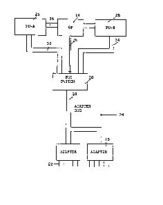
As shown in figure 1, a Control Unit ~10) is usually composed
of a processing unit (12), a service processor (14), a
communication bus or adapter bus (20) ancl a plurality of
adapters (18). The processing unit (12) operates a Control
Program, which is loaded by the service processor (14)
connected to the PU (12) by a control bus (163. Furthermore,
the processing unit ~12) is connected to the adapters (18) by
the adapter bus (20) which comprises a plurality of wires on
which circulate data and control signals exchanged with the
peripheral devices as disk drives, tape drives,...(not shown)
connected to the adapters (18~ by wires (22).
With such a structure where al] the adapters are connected to
a single processing unit (12), the Control Unit (lO) becomes
totally inoperative in case of a failure in either the
hardware of the processing unit (12) or in the Control
Program. The same is true îf the processing unit (12) or the
Control Program has to be stopped for maintenance reasons, and
the reliability of the Control Unlt is accordingly affected.
In figure 2, another known Control Unit structure ~24) is
shown, wherein the processing unit has been split into! two
independent parts (26, 28).
Those independent parts (26, 28) have each a dedicated power
supply, and the adapters (18) are powered by still another
supply, either lndividually or by groups of adapters.
The advantage of thls structure (24) in comparison to the
structure described in figure l consists in the presence of a
bus-switching device l30j connected to the adapter bus t20) on
the one hand, and to each of the independent
Processing Units (26, 28) by separate busses (32, 34). This
bus sw1tching device ~30) allows any processing unit (26, ~8)
to control all the adapters (18), one PU being active at a
given time, the other being standîng by.
The standing-by PU must be ready to take control of the
adapters (18) at any time, so a communication link must exîst
~3~i5~S
s
FR 9 86 020
between both PUs (26, 28), for example through a Service
Processor (14~ connected to each PU part (26, 28) by a control
bus (16~. Thus, the SP (14~ continuously checks the status of
both PUs (26, 28), and in case of a failure of one of the PUs,
it controls the bus~switching device (30) by way of a control
bus (36) in order to have the adapter ~us (20) always
connected to an operative PU (26, 28~ by a bus (32) or (34~.
Consequently, this structure allows to get rid of a single PU
or CP failure. It also allows to a given PU to be stopped for
being serviced, without affecting the operation of the control
unit t24).
However, in this known structure, the bus-switching device
~30) itself is unique, and thus a failure of it would affect
the whole Control Unit operation.
In another known structure this drawback could theoretically
be solved by appending a switching device to each adapter, in
order to attach a given adapter to either one or the other PU,
depending on its availability. But the multiplication of
distributed switches at adapter level is much too complex! and
expensive as soon as the Control Unit comprises a great number
of adapters.
The Control Unit structure t50) shown in figure 3 corresponds
to the principle of the present invention and permits to solve
the drawbacks of both previously described structures ~10,
24). ~ ~
The basic principle consists in using a bus switching device (
called "switch" hereafterj, composed of two identical switch
parts (38, 40). These switch parts are logically independent,
but each one is logically part of its associated PU t26, 28).
.
For the commodity of the explanation, the switch parts ~38,
40) and their associated PUs t26, 28) will also respectively
be called switches A and B ( or SW-A, SW-B ), and processing
units A and B ( or PU-A, PU-B ).
_,,
'
~3~ 5
~. .
FR 9 86 020
As schematically represented in figure 3, the basis of the
Control Unit (S0) according to the present invention consists
in using a partitioned PU comprising (at least) two
independent PU parts PU-A ~26) and PU-B (28), together with a
partitioned switching device comprising (at least) two
independent SW parts SW-A (38) and SW-B (40), said partitioned
switching device being logically associated to the
corresponding partitioned PU.
In other words, SW-A can be-seen as a part of PU-A and is, in
the best embodiment of the invention, powered by the same
source as PU-A (source not represented). Similarly, SW-B can
be seen as a part of PU-B and is powered by the same source as
PU-B.
;~ .
Consequently, no SW part exists which would be related neither
to PU-A, nor~to PU-B.
Prac~ically, it results that the failure of a SW part (either
5W-A or SW-B) would have the same impact on the operation of
the Control Unit, as a failure of its associated PU. That is
to say that in case only one SW part and/or PU part A or B
becomes inoperative, t~e Control Unit can continue to operate,
should~do it with less performance.
For~ using~ the above Control Unit structure (50)
advantageously, the~adapt rs (18) are grouped into two sets
(56, 58)~,~each set being connected to a dedicated adapter bus
52, 54) (primary bus).
:
However, the Control Unit (50) would be of poor interest if it
only comprised two independent PU parts (PU-A, PU B) connected
each to a dedicated adapter bus (42, 52) or (44, 54). The
interest of the SW parts SW-A t38) and SW-B (40) is that they
j allow the swltching of the whole data traffic of the adapter
sets (56, 58) onto one PU part (PU-A or PU-B) when the other
PU part is inoperative.
,.
~L3~S~i
FR 9 86 020
Therefore, as shown in figure 3, each PU part is connected to
its own set of adapters by a primary bus, and to the other set
of adapters by a secondary bus. ~or example, the PU-A is
connected to the set of adapters (56) by the primary bus (52)
on the one hand, and it can on the other hand be connected to
the set of adapters t58j by the secondary bus ~48). Similarly,
the PU-B is connected to the set of adapters (58) by the
primary bus (54) and to the set of adapters (56) by the
secondary bus (46).
Indeed, some device will have to control the switching
operations performed by the switching device, according to the
status of each PU part (A,B) at a given time: operative, or
non-operative because failure or service requirement. The
control of the switching will be done by the SP (14) (Service
Processor), which is known in the prior art (cf CU of the
Communications Controller referenced IBM 3725). This SP (14)
is connected to each PU part (26, 28) by a control bus (16)
which allows it the monitoring of the status of each PU part.
Besides, the SP (14) is connected to each SW part (38, 40) by
a control bus (36), on which switching commands are prolided
to each SW part for changing the connection scheme between the
PU parts (A,B) and the sets of adapters (56, 58) when
necessary (failure of a PU or SW part, service...) In case of
no present failure detected by the SP (14), each PU part A and
B controls its dedicated set of adapters ( respectively 56,
58): this can be called the "duplex normal" operation mode of
the Control Unit. If for example PU-A (26) becomes inoperative
( schematically represented by a dotted cross-line in fi~ure
4), ths set of adapters (56) will be connected to PU-B (28) by
way of the secondary bus (46~ and on request of the SP ~14):
this can be called the duplex fallback-B mode, wherein the
adapters set (S6) previously connected to PU-A falls back onto
PU-B, so that all the adapters be connected to the still
operative PU:-PU-B. Indeed, a symmetrical fallback A operation
mode is entered as soon as PU-B becomes inoperative, if PU-A
remalns operative. It is to be noted that in each fallback
mode, the operation of the adapters connected to a PU part
~L3~
.
FR 9 86 020
(26, 28) by a main bus (42, 44) and a primary bus (52) or (54)
is not disturbed by the switch reconfiguration allowing the
connection of the adapters which are connectled to a secondary
bus ~46, 48).
It is also to be noted that the operation u~der a fallback
mode as previously described~ requires that the control
program operated by each PU (A or B) be configured so as to
enable a given PU part to control both adapters sets (56, 58).
But in what extent the con`figuration of the Control Program
should allow or not a decrease of the performance of the
Control Unit in a fallback mode, is a matter of appreciation
which is outside the scope of the present invention: accepting
a performance degradation in case of fallback, or
under-loading each PU in duplex normal mode, if no performance
degradation can be tolerated in fallback mode. ~
With reference to figure 5, it will now be described how the
basic Control Unit structure shown in figures 3 and 4 can be
generalized and extended to more PUs and switching devices. In
figures 3 and 4, two PUs were considered. As a matter of fact,
the ~described switch structure (50~ can theoretically be
generalized to any number of PUs. For example~ figure 5 shows
how~ three PUs (62,64,661 could be connected, each one
controlling~a set of adapters ~(82,84,86).
The switching device is now composèd of three~ switch parts:
SW-A~ (70),~SW-B !72~, SW-C ~(74). To each signal of a PU bus
~(76) correspond three signals (P, S~ Sl) on adapter busses.
Thus, when a PU fails~ or must be stopped, the adapters
normally~connected to it can be switched to one of the still
operative PUs.``For example, if PU-A or SW-A becomes
inoperative, the set of adapters` (82~ connected to SW-A by
primary bus (78) ~alls back onto SW-B or SW-C by way o
secondary bus- 180), according to the control signal sent by
SP (68) to SW~A, SW-B and SW-C, on control hus (36). However,
a similar fallback operation would be performed i~ another PU
:L3~
, .
.1. 9
FR 9 86 020
part (PU-B, PU~C) or switch part ISW_B, SW-C~ would become
inoperative.
It is to be noted that, for a given PU part becoming
inoperative, the PU-part on which it will fallback may be
determined in advance by any means, for example by fallback
tables memorized by the SP.
;~ ~Although this structure can in theory be generalized to any
number of PUs, it will be limited in reality, by the numbex of
adapters to be connected to the PUs, and by the growing
complexity of the SP (14) which will have to command the
different SW parts.
It should be understood that the Control Unit according to the
invention is not meant to be limited to a very specific
; control unit, for ~instance a communications controller. In
such an application, the adapters are the channel adapters of
the communications controller, which connect the
Communications Controllex to a Host computer~ and the line
adapters which connect the communic ations controllel to
transmission lines through modems, while the Central Control
Unit~of the communications controller is equivalent to the PU
in the~ present specification. However, although the
application of the invention to the Central Control Unit of a
communications controller is very advantageous, the control
unit of the invention can be fully described in more general
~ ~ ~ terms, as will be done farther.
:: : .
Figures 6 to 9 rel~ate to a basic Control Unit structure
according to the invention, said Control Unit comprising two
duplicated PU parts PU-A, ~PU-B and two duplicated SW parts
SW-Aj SW-B as previously shown in figures 3 and 4. Generally
speaking, the husses (42,44,46,48,52,54) (figures 7,8) to be
switched contain a given number of bidirectional data wires
and outgoing or ingoing signals, the "out" direction of the
signals corresponding to signals going from the PU toward the
adapters.
s~ ~
FR 9 86 020
It is ~o be noted that in some communications controllers, the
corresponding busses contain 16 data wires and about 15 wires
for the transmission of tags or commands~ But in the present
invention, said busses may contain any number of data or
command wires, and the corresponding data a commond will more
generally be called "signaIs".
If it is necessary to make a change of the Control Unit
configuration consecutive to a PU part failure, the SP (14)
(figure 3) will transmit thë right commands to the Switch and
accordingly, the SW part 138,40) will perform the needed
switching of the busses (46,48,52,54). Figures 6 and 7 show
how the switching commands are transmitted from the SP (14) to
the switch parts PU-A, PU-B. Each SW part contains a Switch
Configuration Register SWCONF-A (88) or SWCONF-B (90), the use
of which will be described farther.
~Figure 7 shows in greater detail the structure of the Control
Unit_1n relation to the outgolng signals (from the PUs and SP
to the adapters). Each PU part (26,28) is connected to the SP
(14) by a control bus permitting to the SP to be informed of
the status of e~ach PU (operative, non operative...). PU-A t26)
~and PU-B~ (28) are respectively connected to SW-A (38) and SW-B
`(40) by a bus (42,44) on which outgoing signals are sent
through the Switch parts~toward the adapter sets (52,54).
These~outgoing~signals are received by receiver circuits (100)
which~ do ~not~ have any ~logical; function, but perform the
technologica1 adaptati~on (voltage levels,...) between the PUs
and the -adapt~ers if ~ecessary. Such receiver circuits are
well-known in the art~ Accordingly, they are not urther
described in the present specification.
The output of each receiver circuit ~100) is applied in
parallel to a gating circuit (104,106) in SW-A (or (108,110)
in SW-B) comprising two AND gates (104,106) or (108,110). The
second input of each AND gate (104,106) receives a gating
signal PA and SA (or PB and SB) transmitted by Switch
Configuration Register SWCONF-A (respectively SWCONF-B)
~ 3~PSSSS
11
FR 9 86 020
composed of two latches (92,94) (respectively (96,98) for
SW-B).
Again, drivers (102) are needed for transmitting the signals
outputted by AND gates (104,106,108,110) to the adapter sets
(52,54) which may be separated by a distance of several
meters from the SW parts SW-A, SW-B of the Control Unit.
It appears that, according to the binary value (0 or 1) set
into ; each latch (92,94) of SWCONF-A, the signal
transmitted by PU-A on wire (91) will be outputted by SW-A on
wire (105) and/or (107). Thus, according to the content of
SWCONF-A, the signal on wire (91) will be outputted toward
adapter set (56) on primary bus (52) (normal operation mode),
or toward adapter set (58~ on secondaxy bus (46) (fallback-A
mode), and/or toward both. Similarly, aocording to the content
of SWCONF-B, the signal on wire (95) will be outputted toward
adapter set (58) on primary bus (54) (normal operation mode)
and/or toward adapter set (56) on secondary bus (48)
(fallback-B mode) and/or toward both.. Thus, for each outgoing
signal (91,95), the operation performed by a switch part
SW-A,SW-B) consists in transmitting said outgoing signal
(91,95) to the corresponding adapter set (56 or 58), or to
both in case of a fallback mode.
All~the possible si.tuatlons are shown in f~lgure 6, where all
the valid contents of the~ SWCONF registers A and B are
represented. For example, if latches (92,94) of SWCONF-A are
respectively set to 1 and 0, the signal outputted by PU-A on
wire t91~ will be gated only through AND gate (104) and
transmitted to one (or several) adapters of adapter-set (56~.
Further, if latches (96,98) of SWCONF-B are respectively set
to 1 and 0 too, the signa~ outputted by PU-B on wire (95) will
be gated only through AND gate (108) to one (or several)
adapters of adapter-set (58).
This situation corresponds to the "normal mode", where:in each
PU part and SW part is in relation with the adaptar-set
:~3a5s~5
; 12
FR 9 86 020
connected to lts own primary bus. On the contrary, if for
example PU-B is inoperative, the adapter-set (58) can only be
addressed by PU-A through SW-A. This requires that the latches
(92,94) of SWCONF-A be both set to 1, so that the signal
outputted by PU-A on wire (91) be transmitted by SW-A to
adapter-set (56~ on primary bus (52), and to adapter-set ~58)
on secondary bus (48). But in the mean time, the latches
(96,98) of SWCONF-B must be both set to 0 in order to avoid
logical conflicts between busses (52) and (46~, or ~54) and
(48j.
Figurè 7 shows that the setting of logical values into the
latches (92,94,96,98) of both SWCONF registers is performed by
the SP (14) through command busses (36). Indeed, the SP
chooses automatically ~by software) the right values to be set
into said latches, according to the status of each PU part, as
detected by said SP.
Thus L the SP chooses~ the best operation mode (normal,
fallback,...~ in order to maintain the Control Unit operative,
and loads the latches (92,94,96,98) accordingly. It is to be
noted that, although one wire (91) and one gating circuit
~(104,1Q6) have been represented, the SW-A contains as many
wires and gating clrcuits of that type, as there are outgoing
signals transmitted by PU A. However, the SW-A contains only
one SWCONF register,~comprising two latches (92,94) providing
. .
the gating~signals PA~(i.e relevant to primary bus connected
to SW-A) and SA (i.e relevant to secondary bus connected to
SW-A). Similar remarks are true for the SW-B~
Figure 8 shows how the ingoing signals provided by the
adapters are transmitted to the PUs PU-A and/or PU-B according
to their availability. In accordance with the principle of the
~present invention, each set of adapters transmits the ingoing
signals to b~th SW parts A and B in parallel. Each SW part
comprises one selecting circuit (111,115) per primary t99) or
secondary (101) incoming wire. The incoming signals are
transmitted to the select:ing circuits ~111,115) through
~3~ii5~iiS
13
FR 9 86 020
receivers (103) which, again, perform the technological
adaptation of the signals to the PU technology, and are known
in the art. The operation performed by the selecting circuits
(111,115) consists in selecting the adapter-set which will
have its incoming signals transmitted to a given PU, in
accordance with the content of the SWCONF register of said
given PU. For example, the selecting circuit (111) of SW-A
decides whether an incoming signal on a wire (99) of primary
bus (52) will reach PU-A, or whether an incoming signal on a
; wire l101) of secondary bus (48) will do so.
Therefore, the selecting circuit (111) of SW-A comprises, for
each pair of incoming wires of busses (52,46), two AND gates
(112,114) having each an entry connected respectively to a
wire (99) of primary bus (52) and a wire (101) of secondary
bus (48). Furthermore, the other entry of each AND gate
(112,114~ is respectively pro~ided by the SWCONF-A register
~(92,94), with the PA and SA signals, these signals enabling
the gating of either a signal provided on wire (99) (by
adapters-set (56)) or a signal provided on wire ~1013 ~by
adapters-set (58)) toward an OR gate (120).
Consequently, at the output of OR gate ~120) of selecting
circuit (111) of SW-A, either an incoming signal from primary
adapter bus~(52) or an incoming signal from secondary adapter
bus ~48) is~ transmitted to~PU-A for being processed. For a
better adaptation of logical levels, this transmission is
~ preferably made through a driver (102) similar to the drivers
(102~ mentioned in relation to figure 7.
,~ :
It is clear that the selecting circuit (115) of SW-B has the
same function as selecting circuit (111) of SW-A and
~accordingly it is symmetrically composed of AND gates
(116,118) connected to OR gate (122).
Figure 9 shows how bi-directional signals are transmitted
between the PUs PU-A, PU-B and the adapter-sets.
~3~ii5~i
,. ~ . . ` .
. 14
FR 9 86 020
The structure of the SW parts for each bi-directional line,
is shown. Thus~ SW parts SW-A and SW-B of the Control Unit are
in fact, for each bidirectional signal, a combination of the
structures shown in figures 7 and 8 for respectively outgoing
and ingoing signals, said structures being connected in
parallPl.
For example, for each bidirectional signal to be exchanged by
PU-A and an adapter-set, SW-A comprises for the outgoing
direction: a receiver circuit (103) connected to a wire (91)
of primary bus ~42) and a gating circuit composed of AND gates
(104,106) for gating an outgoing signal toward primary bus
(52) or secondary bus (48) through drivers (102).
For the transmission of ingoing signals from one of the
adapter-sets toward PU-Ar SW-A comprises receiver circuits
(100) having their entries (140)~ connected in parallel with
the outputs (142~ of the dri~ers (102) used for the
transmission of the outgoing signals.
Similarly to figure 8, these receiver circuits (100) have
their outputs connected to one of the inputs of two AND gates
(112,114), the outputs of which are ORed by OR gate (120). The
output of OR gate (120) is then transmitted toward PU-A
through a driver (102).
It is clear that the~SW-B has the same structure as SW-A and
performs the same switching function, but between PU-B and the
adapter-sets.
However, for transmitting bi-directional signals on some of
the~wires between each PU part and its primary or secondary
adapter-set, it is necessary that the direction of
transmission within each switch-part be indicated at every
moment. Consequently, a specific outgoing signal W (write)
provided continuously by PU-A on line l144) is used, being
understood that a symmetrical means is used within PU-B (line
146~. This W ~ignal alone is used as an enabling command or
~3~5~
FR 9 86 020
receiver (103) (figure 9). This W signal is also inverted by
inverter (130) which accordingly delivers a Read signal , used
as an enabling command for driver (102~ connected in parallel
to said receiver (103).
Furthermore, the Write signal W is ANDed with the PA and SA
signals provided by the SWCONF-A register as described before,
by respective AND gates (132) and (138). This results into two
command signals P.W and S.W applied respectively to one entry
of AND gates (104,106~. Similarly, the Read signal R is ANDed
with the P and S signals provided by the SWCONF-A register, by
respective AND gates (134) and (136). This results into two
command signals PA.R and SA.R applied respectively to one
entry of AND gates (112,114).
From this structure it results , according to the permitted
values of PA and SA as shown in figure 6, that if the W signal
on line (144) is high (W=1~, the signal on line ~91) will be
in the outgoing direction, and will be transmitted toward the
primary bus ~52) or secondary bus (48) according to the value
of the PA and SA signals transmitted to the SW-A by the S~.
.
For example, if W = 1 and PA = 1 while SA = 0 (normal mode),
the signal transmitted by PU-A will cross the receiver ~103)
and reach AND gate tl04~. There, since PA.W = 1 and SA.W = ~,
; it will only be gated:through the driver (102) connected to
:AND gate II04), and thus, it will reach the primary bus (52)
~~lead~ing toward the primary adapters-set.
In another example, if W = 1 while PA = 1 and SA = 1 (fallback
mode on PU-A~, the signal transmitted by PU-A will cross both
AND gates (104,106) since PA.W = 1 and SA.W = 1. Thus, it will
reach both the primary bus (52) leading to the primary
adapters-set, and the secondary bus (48) leading to the
adapters-set connected to PU-B and SW-B.
In still another example, for an ingoing signal to be
transmitted by an adapter set, to one of the PUs PU~A or PU-B
~3~5~S~5
. ~ .
FR 9 86 020
according to the decision of the SP, said ingoing signal will
reach a given PU only if the Read signal is high: R = 1.
If the incoming signal is provided by the primary adapter-set
(56) (figure 4~ on a wire of primary bus (52), it will be
applied to both the SW-A and the SW-s (on secondary bus (46)).
Thus it will reach the inputting receiver (100) of SW-A and
the inputting receiver (150) of SW-B. Then, if PA = 1 and SB =
0 Ifallback-A mode), the ingoing signal will cross AND gate
(112l of SW-A and reach PU-A through OR gate (120) and driver
(102), while said signal will not be able to cross AND gate
: (118) of SW-B, since SB = 0 and SB.R = 0 (with positive
logic).
Of course, all the possible operation phases of the SW parts
SW-A and SW-B will not be described herein, but could easily
be obtained with the previously described structure of the
switch, if the signals PA, SA, Ps~ ss and W, R are given all
the valid values.
However, among the 16 different combinations of values PA, SA,
PB, SB, some are not valid, because they would lead to
conflicts on busses. For example if W = l (outgoing signals)
and if PA = 1, the SB signal available in SW-B must be low: if
the logical value of SB became equal to l while PA = 1, it
wouId mean that both SW parts could transmit outgoing signals
on busses~52) and ~46) through respective drivers (102) and
:(152) (figure 9). This would lead to conflicts on bus l52)
~ ince bus (46) is connected to it.
Besides, since drivers (102) and ~152) have their outputs
connected to:gether through busses (52, 46), they must be
technologically glitch-less when powered up or powered down,
and must present a high impedance when powered down, in order
to avoid interactions. Indeed, the same remarks are true for
the dr.ivers connected to bwsses (54, 48)~
Although the structure of the Control Unit as detailed with
reference to figure 9 permits to obtain the basic switchi.ng
function between two PUs and two adapter~sets, the best
_.
~3~
: 17
FR 9 86 020
embodiment of the invention comprises several additional
features for a more reliable operation of the Control Unit.
I~hese additional features will now be described; with
reference to figures 10 to 14.
In all the previous developments, it was assumed that it is
always possible for the SP to accede to the latches (92, 94,
96, 983 of the SWCONF registers for defining the operation
mode of the Control ~nit. However, this may be difficult in
some cases, and the additional features that are provided are
aimed to enable a very reliable loading and controlling of
said SWCONF registers. In the Control Unit, the actual
configuration status of each switch part is contained in its
SWCONF register ( figure 9 ). It would be quite dangerous, as
far as the availability of the system is concerned, to alter
the content of the SWCONF registers by simple Write commands
issued by the SP (14~.
:,
Thus, a more complex procedure must be followed by the SP,
:including confirmations of the various contents of the command
registers, :for minimizing :unexpected SWCONF registers
modifications: due to hardware or software failures in the
Service Processor.
Thls~aim ~lS achieved with~the status control means shown in
figure 10, related~to only:one SW:part (for instance SW-A) for
more simplicity, being understood:that the same features exist
within SW-B.
The SW-A comprises two additional registers NEWCONF t NEW
CONFIGURATION~3 and ACTCONF ( ACTIVATE CONFIGVRATION ), each
of which comprises two cells (190, 191) and (200, 202). These
registers NEWCONF and ACTCONF are made accessible through
wires (201,203-,205,207j to the Service Processor (not shown) ,
which may modify their content, in order to allow any change
of switch confi.guration (fic3ure 10). Thus, NEWCONF register
(190, 191) can be loaded With the P,9 bits corresponding to
~3~ iS
1~
FR 9 86 020
the expected configuration, and ACTCONF register (200, 202)
must have the same new configuration pattern as the one
specified in NEWCONF, when an ACTSW (ACTIVATE SWITCH) latch
~218) is set ON. The event of NEWCONF and ACTCONF having the
same content is tested by comparators (204,206), the outputs
of which are ANDed in AND gate (208), together with the status
of ACTSW latch (218)o
Besides, the contents of SWCONF and NEWCONF registers are
compared by XOR circuits ~210, 212), the outputs of which are
applied through WORKCONF register ~224, 226) (later
explained), to AND gates (214, 216), together with the output
of AND gate (208) mentioned above. As a result, the new values
(P,S) for the determination of the new con~iguration of the
SW, are gated from the NEWCONF register (190, 191) into the
SWCONF register (192, 194) only if the new configuration is
different from the one present in the SWCONF r`egister , and if
the SP simultaneously gives ( by means of ACTCONF and ACTSW )
an authorization for transferring the new configuration into
the 5WCONF register (192 r 194)-
Any mismatc~ between NEWCONF and ACTCONF will keep the SWCONFunchanged.
Similarly, SWCONF is altered only if NEWCONF and ACTCONF
pa~tterns are dlfferent from the pattern of bits present in
SWCONF.
NON DISRUPTIVE SWITCHING OPERATION
In the above description, the SWCONF register of a given SW
part is updated as soon as ~the SP has loaded NEWCONF and
ACTCONF with the values corresponding to the new configuration
expected, and ACTSW latch has been set ON.
In fact, it is important to be sure that this operation is
non-disruptive. As an example, if a SW configuration change
must be performed from duplex normal mode to fallback-B rnode,
~3~
19
FR 9 86 020
this change must not disturb the operation of PU-B with its
own adapters-set (58~ (figure 7). In this example it is
therefore necessary to perform the configuration change while
there is no activity on the adapter-bus driven by PU-B through
SW-B. Two possible alternatives are then to be considered as
far as the main busses (42,44) connected between the Switch
parts and the PU parts are concerned:
- Upon SP control, a specific "bus disable" line (not shown)
can be raised by the SW part to its associated PU part just
before a configuration change is to be don~ by the Service
Processor. The PU must then terminate its current data
*ransfer (if any) and stop serving any new transfer request
~rom adapters. The configuration change thus takes place
during a "switching window" defined by hus disable line being
active, and no data transfer being granted any longer.
.
- More currently, it is not possible to add a new bus line (as
previously the "bus disablei' line). However, conventional bus
control lines exist to indicate that a bus activity is in
progress, and thus permit to design a feature ensuring a
non disruptive switching operation.
Such a bus control line called "operation in progress" (225),
is shown in figure 11. It is activated by the PU at the
beginning of each data transfer. In this case, the switching
window is defined by the fact that the "operation in progres"
line is inactive.
Figure 12 shows how the "SWITCHING WINDOW" signal is used as
an entry to AND gate (208), the output of which must be high
for enabling the content of SWCONF (192, 194) to be changed by
NEWCONF (190, 191).
However, a switching window (during which the values of P and
S may be modified, to change the Control Unit operation mode),
is defined by a logical combination of the contents of NEWCONF
register (88) and the I/O line (225), as shown in figure 11.
iiS~i;5
.. ..
FR 9 86 020
More accurately, the outputs of AND gates (228, 230) transmit
the right values of P and S, which determine the operation
mode after switching, provided that the inputs of said AND
gates (228, 230) receive the adequate values: I/O line (225)
high (i.e PU inactive), output of inverter (234) high, and
SWCONF registar (88) containing the same values as NEWCONF
register.
However, it is necessary to get rid of the ca~e in which
"operation in progress" line would become active just after
the switching window has been activated. Therefore, a WORKCOMF
register (224, 226) is provided, the content of which is
different from (0,0) only when NEWCONF is different from
SWCONF (configuration change in progress). The outputs of both
latchas ~224, 226) are ORed by OR gate (232~ and inverted by
invertar (234). Thus, the output of inverter ~234) is high
only if both WORKCONF latches are zero. This event is used to
allow the propagation of "operation in progress" signal on
line_(225) through AND gates ~228, 230).
~; ~As long as WORKCONF is not all zero, the output of inverter
(234) inhibits propagation of "operation in progress" signal,
thus allowing a configuration change~
RESET LINE
When the SP decides to perform a switching action from duplex
to fallback mode after ~a failure of one of the PUs, the
adapter-bus connected to the failing PU, which is to ba
switched onto the still~operative PU, i5 in an unknown state.
Therefore, it is necessary to perform an adapter-bus Claar
operation, before changing the SW configuration. This is done
by activating a special adapter-bus line called RESET line
(figure 13). When receiving this signal, each adapter clears
its bus interface, i.e no more control in, data, request or
interrupt lines are active on the adapter-bus, and thus each
adaptar connected to the failing PU i8 ready, once the
~3(~ i5
FR 9 86 020
adapter-bus has been cleared, to accept a command from the
still operative PU after switching.
This adapter-bus Clear operation is mandatory to avoid any
disturbances on the adapter-bus onto which the adapter-bus
presently in trouble will be connec~ed after the switching.
Normally, the resetting of the adapter bus connected to a
given PU part and SW-part should be done by the SP through
said SW-part. ~ : -
.But it may happen that the failure which needs a fallback be
such that the SP cannot use the RESET line of the failing
SW-part to clear the corresponding adapter-bus.
This is particularly the case if the failure is due to one of
the SW~part~ land not to a PU-part). To allow an Adapter Bus
Clear operation in all cases,~ the SW structure is such that
the SP can clear any adapter-bus through any SW part,
reg~ardless of the SW co~nfiguration.
To achieve this, each ~SW part comprises, as shown in figure
13,~ a BUSCLEAR register (2~), accessible by the SP, said
BUSCLEAR register being able to generate a RESET-P signal, and
a RESET~S signal. For more reliability when a reset signal has
to ~e generated, each BUSCLEAR register comprises four bits:
two Busclear bits (1,2)~ must ~be simultaneously active to
activate the RESET-P signal, and two Busclear bits (3,4) must
be~simultaneously actlve to activa~te the RESET-S signal.
This allows to SP running diagnostic programs (out of the
scope of the invention) to perform a complete BUSCLEAR
register test without~actually generating a RESET signal,
simply by reading back one bit of BUSCLEAR register after the
other and ch~cking it. The RESET-P and RESET-S signals are
respectively outputted of the SW parts as particular lines of
primary busses ~52,54) or secondary busses (46,48) as shown in
figure 3.
~3~ 5
22
FR 9 86 020
DISCONNECT SWITCH
Further, in case of a severe failure in a SW part (SP control
bus failure or SW part internal error), it is necessary to
have a DIRECT way to disconnect the adapter bus from this SW
part in order to allow a fallback reconfiguration.
Therefore, as shown in figure 13, the SP uses two special
lines (250, 252), one per SW part, called "DISCONNECT SW-A"
and "DISCONNECT SW-B". -
In each SW part, the corresponding "DISCONNECT SW" signal islatched into a "DISCONNECT LATCH" t254, 256), the output of
which is ANDed ( AND gates 260,262,264,266) respectively with
the PA, 5A, PB, SB signals provided by the SWCONF registers
(not shown). Whatever the status of said PA, SA, PB, SB
signals is, :any outgoing or bidirectional line (268,270) can
be logically disconnected, as soon as a DISCONNECT LATCH
(254L256) sends a "zero" to AND gates ~272,274,276, 278)
through AND gates (260j262,264,266).
This is equivalent to a physical disconnection ( such as SW
part powered-off or removed) of the SW part corresponding to
the active DISCONNECT LATCH.
Furthermore, each latch (2-54, 256) can be reset by a command
sent from the other SW part on lines (280, 282), said command
resetting the status of the DISCONNECT LATCH of a given SW
part ( which is equivalent to a reconnection of said SW part).
The reset command sent by a given SW part to the other SW part
is generated by two dedicated registers RDISC (Reset
Disconnect) (284) for SW-A and (286) for SW-B, and CRDISC
(Confirm Reset Disconnect) (288) for SW-A and (290) for SW-B.
For a better reliability and serviceability, two bits must be
active in both RDISC and CRDISC re~isters of each Switch part~
~3~5~;S
FR 9 86 020
in order to be permitted to reset the DISC latch of the other
SW part.
According to the previously described features, a switching
operation from duplex normal mode to duplex fallback-B mode
(for example, if PU-A became inactive) would require following
stages:
1. Clear the adapter bus (52) connected to the inactive PU
part (26), in order to avoid conflicts on said bus (due to
erroneous values) when it is going to be connected to the
active PU part (28).
2. Disconnect the adapter bus (52) from the inactive PU part
(PU-A). This would require:
- writing zeroes into the NEWCONF register ~88) o~ the SW
part ~S~-A) corresponding to the failing PU part (PU-A).
_
- writing zeroes into the ACTCONF register (200,202) of the
same SW part (SW-A).
- setting ON the ACTSW latch (218) of the SW part
corresponding to the failing PU part.
If these operations revealed unsuccessful (i.e SW-A also
inoperative), it would be necessary to issue a DISCONNECT
SWITCH command through the SP (as explained in relation to
figure 13), in order to have PU-A really disconnected from its
dedicated adapter bus (523.
: ~ .
3. Connect adapter (52) to the still active PU part (PU-B)
through secondary bus (48).
This means t~at all the adapters of adapters-set (56) fall
back onto PU-B. This operation would require following
operations to be done by the Service Processor:
~3~ 5
24
FR 9 86 020
- writing all ones into the NEWCONF register (90) of the 5W
part(SW-B) corresponding to the still active PU ~PU-B).
~ writing into ACTCONF register of SW-B, the same pattern as
the one contained in NEWCONF register of SW-B.
- setting ON the ACTSW latch of the same SW part (SW~B)o
- resetting the ACTSW latch of said SW part (SW-B).
Once these operations have been done by the SP , the Control
Unit is in fallback-B mode, and all the adapters of both
adapter-sets ~56, 58) are connected to PU-B through SW-B. This
permits to PV-A to be fixed, if necessary, and then a reverse
switching operation can be done: from duplex fallback-B mode
to duplex normal mode, with~two phases analog to those
previously described:
- Disconnect the secondary bus (48) connectinq the set of
adapters (56)~ to the active PU part (PU-B).
- Re-connect said set of adapters (56) to the other PU part
(PU-A~ by primary bus (52).
It~is to be~noted that the switching from duplex fallback to
duplex normal~:mode does not require, at first, the adapter bus
to be cleared: since it was connected, just before, to an
active PU, it normally should not contain erroneous logical
levels on its lines. ~
: ~ :
_.