Note: Descriptions are shown in the official language in which they were submitted.
~ ~3CJ1~77~7
Circuit arrangement having a plur~lity of electrical ele~ents to
be cooled
:
The invention relates to a circuit arrangement in accordance
with the classifying part of patent claim 1.
It is an o~ject of the 1nvention to provide a circuit
arrangement of compact construction which is electrodynamically
sta~le even ~ith low-reæistance high-current circuits, which
ensures optimum, oven cooling of tha elements and only requires
one cooling medium inlet and one cooling mediu~ outlet
~onne tion, without addition~l cooling medium piping and
~ i :
fittings being required.
::
The present inv~ntion r~Iates to the solution of this problem.
:
:~ j
, ': :
'~
'
`
~3~ 77
- 2 01559-94/PATENToAMD/LCS/fs
Su-rnmary of the Invention
In one aspect of the invention, a circuit arrangement of compact
construction giving even cooling of the elements include a
transformer having at least one secondary winding with a center
tapping and a plurality of rectifier elements. Provlded are a
plurality of substantially plate-like electrical conductors for
electrically connecting -the rectifier elements. The plate-like
electrical conductors have channels therethrough adapted to carry
a cooling medium for cooling the rectifier elements. A cooling
medium distributor is provided in the Eorm of an electrically
conductive substantially rectangular bar having a Eirst and a
second side which are opposite to one another, and a third side,
and having an inlet cavity and an outlet cavity Eor a cooling
medium, with the inlet cavity being in -the first side and the
outlet cavity being in the second side. The elec-trical conductors
and the rectifier elements are arranged in rows along the ~Eir~st
side and the second side of the distributor. Means are provided
~or holding the dis-tributor and the rows of the conductors and
rectifier elements ~together in sandwich-like manner with the
distributor in the middle. The third side o~ the electrically
conductive cooling medium distributor is electrically connec-ted
with the center -tapping oE said secondary winding.
In another aspect of the invention there is provided a circuit
arrangement having a transformer which has a plurality of
secondary windings each having a first end tapping and a second
end tapping. A cooling medium dis-tributor includes a bar having a
;`
. . ~
~3C~777
- 2(a) - 01559-9 4/PATENT . AM~/LCS/f S
first side and a second side which are opposite to one anotherO
The cooling medium distributor has an inlet cavity and an outlet
cavity for a cooling medium with the inlet cavity being in the
first side and the outlet cavity being in the second side. A
group of rectifier elements for each secondary winding is provided
with each group including first and second rectifier elements
arranged opposite to one another at the Eirst side and at the
second side of the distributor. ~ plurality of electrical
conductors are included for electrically connecting the rectifier
elements. The plurality of electrical conductors have channels
therethrough adapted to carry a cooling medium Eor cooling the
rectifier elements, and each of the Eirst rectifier elements are
disposed between a Eirst pair of the electrical conductors and
each of the second rectifier elements are disposed between a
second pair of the electrical conductors, so that for each
secondary winding there is a respective group of first and second
rectifier elements and a respective group of first and second
pairs of electrical conductors arranged opposite to one another at
the first side and at the second side of the distributor. The
electrical conduc-tors and the rectifier elements are arranged in
rows along the first side and the second side of the distributor.
The distributor and the rows of the conductors and rectifier
elements are held together ln sandwich like manner with the
distributor in the middleO The first end tapping oE each
secondary winding is electrically connected with one electrical
conductor of each of -the ~irst pairs of electrical conductors
associated with the respective secondary winding. The second end
tapping of each secondary winding is electrically connected with
i777
~ - 2(b) - 01559-94/PATENT.AMD/LCS/fs
one electrical conductor of each of the second pairs of the
electrical conductors assoclated with the respective secondary
winding.
In yet another aspect of the invention~ a circuit arrangement
includes a transEormer having a secondary winding with a first end
tapping and a second end tapping. A plurality of rectifier
elements is provided and a plurality oE substantially plate-like
electrical conductors for electrically connecting the rectiEier
elements is included. The plate-like electrical conductors have
channels therethrough adapted to carry a cooling medium for
cooling the rectifier elements. A cooling medium distributor in
the form oE a bar having a Eirst side and a second side~ opposite
to one another, and having an inlet cavity being in the Eirst side
and the outlet cavity being in the second side. The electrical
conductors and the rectifier elements are arranged in rows along
the first side and the second side of the distributor. The
distributor and the rows of the conductors and rectifier elements
are held together in sandwich-like manner with the distributor in
the middle. Each of the rectifier elements are disposed between a
pair of the electrical conductors. The first end tapping of the
second winding is electrically connected wi-th one electrical
conductor of each pair of the electrical conductors arranged in
the row at the Eirst side of the distributor and the second end
tap~ing of the second winding being electrically connected with
one electrical conductor of each pair of the electrical conductors
arranged in the row at the second side of the distributor.
;7~
- 2(c) - 01559-94/PATENT.AMD/LCS/fs
There follows a more detailed explanation of an embodiment of the
invention with re:Eerence to the drawings. There are shown in:
ig. 1 an electrical circuit diagram of a circuit arrangement
of a three-phase transformer with semiconductor diodes,
ig~ 2 a perspective representation of part of the circuit
arrangement of Fig. 1, _ / ,
/
~,' /
: /
:: /
/
, /
::::~ :
57~7
Fig. 3 a side view of the pressure plates of the circuit
arrang~ment,
Fig. 4 a section in the plane shown in Fig. 2 with ~ broken
line in the direction of the arrow IV.
The circuit arrangement may be used in a DC resistance
weldin~ machine. It consists of a three phase high-current
transformer 4 having primary wintings 5, 6, 7 and second~ry
windings 1, 2, 3. The sacondary windings 1, 2, 3 are connected
at the ends to copper bars 101/102, 201/202 and 301/302 and with
in ~ach case one middle tapping to a middle tapping bar 13 (of
copp~r) (Fig. 1, 2, 3). PressQd thereto by means of screws (not
æhown) is ~ middle bAr 8 so that the bars 8 and 13 ara joined in
an electrically conductive and mechanically stable manner. The
bars 101, 201, 301 are disposed aligned together in a row
parallel to the bar 13 to the right side thereof shown in Fig. 2
and insulate~ a~d distancad therefrom by an insulating plate 53
~Fig. 2 ~nd 3), The bare 102, 202, 302 are correspondingly
disposed in a row to the left side of the bar 13 and separated
therefrom by an insulating plat~ 54. The bars 13, 101, 102, 201,
202, 301, 302 and the insulating plates 53, 54 thus form a
package disposed on the front side of the transformer 4. An
iDSUlAting foil 55 and 56 is disposed batween th0 surface of the
row of bars 101, 201, 301 and/or 1~2, 202, 302 away from the
tr~nsformer and other parts of thQ circuit arrangement t~ be
described b-low.
.
!
~3~
-- 4
Rectification is effected in each case ~y four semiconductor
diodes for the half wave of each phase. The polarity of the
output voltage to the output conductors of the diodes formed by
elongated plates 9, 10 is positive, but can, however, be ch~nged
over to negative if required by fitting all the diodes with into
their holders with reversed polarity~
The total of twenty-four diodes are disposed in two rows of
twelve diodes e~ch on both sides of the middle bar 8 and
designated by three-digit referen~e numbers beginning with the
num~er 1. The second numbers .1. to .3. designate the phase, the
third numbers are A continuous numbering from ..1 to ..4 for the
diodes to the right of the middl~ bar 8 and ..5 to ..8 for those
on the left side.
The removal of the dlssipated heat of the diodes 111 to 13~ is
e~fected by means of cooling water flowing in the electric~l
conductors. The rectangular middle bar 8 has on its lower end
face one connection each 17, 18 for the inflow and outflow of
cooling water which open directly into cavities 11, 12 in its
interior. The cavities 11:, 12 are designed as U-shaped cut-outs
opposite to one another, whar~by the cavity 11 in Fig. 4 is open
to the left and cavity 12 to the right and the two cavities are
separated from one another by a crosspiece 19, the width of
which is sufficient to take up through holes for screws ~not
:~L3~7~
shown) for securing the middle bar ~ to the ~iddle tapping 13.
The cooling water is sealed in the cavity 11 from the plAte 10
by means of a sealing and insulating fo:il 52 lying between the
middle bar 8 and the plate 10 and, analogously, the cavity 12 is
sealed from the plate 9 by means of a sealing and ins~lating
foil 51. Since the middle bar 8 hae a different potential to the
two plates 9 and 10, the sealing and insulating foils 51, 52
provide electrical insulation as w~ll as liquid sealing.
The plate 9 with the foil 51 and the plate 10 with the foil 52
are each screwed onto one side of the middle bar 8 with an
assembly constructed in layers containing a diode by means of
four screws 20 for each assem~ly. Each asssmbly comprises from
inside to outside an inner connection conductor plate adjacsnt
to the plate 9 or 10, the diode with resilient intermediate
plate, an outer connection conductor plate, a twin conductor, an
outer insulating oil and a pressure plate.
~' :
The connection conductor plates resting against the electrodes
(cathode and anode) of the diode are hereinafter referred to as
electrode pl~tes.
, :
The deoignation of the two electrode plates, the resilient
intermediatQ material, the ~wo connection pieces, the outer
insulating foil and the pressure plate follows that o~ the
diodes with threa-digit referenca num~ers, wherQhy the innQr
'.
777
-- 6
electrode plate hetween diode and plate 9 or 10 is gi~en a
number beginning with the figure 2.., the following resilient
intermediate plate beginning with 7.., the outer electrode plate
beginning with 3.., the twin conductor beginning with 8.., the
outer insulating foil beginning ~ith 6.. and th~ pressure plate
beginning with 4.... The assembly composed of the inner
electrode plate 211, the outer electrod~ plate 311, th~
resilient inte~mediate plate 711, the twin conductor 811, the
outer insulating foil 611, the pressure plate 411 ancl the dioda
111 is secured with the plate 9 and the sealing and insulating
foil 51 by the four ~crews 20 to the middle bar 8 by means of
the pressure plate 411 as counter plate. In order to achieve the
pre~sure required ~r a good electrical contact of the diodQ 111
the pressure plat~ 411 has a pressure screw 14 with a cylinder
head 15, a pressure spring 16 and a pressure washer 21.
Similarly, the remaining assemblies c~ntaining the diodes 112 -
114, 121 - 124 and 131 - 134 are secured with the plate 9 and
the foil 51 and the assemblias containiny the diodes 115 - 118,
. ~
; 125 - 128 and 135 - 138 aro secured with the plate 10 and the
foil 52 to the right or left side of the middle bar 8.
The screws 20 are conductive and contained in insulating sheaths
80 that th~ pressure plates 411 - 438 have the same electrical
.~ potential as the middle bar ~ and the intermediata parts are
~, i
insulated from the plates 411 - 438 and the bar 8. Plat~s 9 and
10 and the inner electrode plates 211, 212, .., which are
I
, I
~3~ 7
insulated ~rom the ~iddle bar 8 and the outer electrode plates
311, 312 by means of thQ insulating foil 51 and the intermediate
plate 711, 712, ... have the same potential. Of similar
potential are the outer electrode plates 311, 312, ... with the
twin conductors 811, 812, ~.., which are insulated by maans of
the insulating foils 511, 612, ... from the pressure plate 411,
412, . and by ~eans of the intermediate plate 711, 712, ...
from the inner electrode plate 211, 212, ....
The diodes 111 to 114, 121 to 124 and 131 to 134 lie :Elat
immediately against the relevant inner alectrode plAtes 211 to
214, 221 to 224 and 231 to 234 and these, in turn, lie against
the plate 9; the remaining diodes 115 to 118, 125 to 128 and 135
to 138 lie ~y analogy against the plates 215, 216, ... and these
against the plate 10. Both plates 9 ~nd 10 have the same
electrical potential and are only separated from one another on
tha basis of the mechanical construction.
The electrical conne~tion of the diode anodes to the bars 101,
102, 201, 202, 301, 3G2 connected ~ith the secondary wlndinys 1,
2, 3 of the transformer 4 i~ effected by means of the twin
conductors 811, 812, ... and tha outer electrode plates 311,
312, .... Tha twin conductors 811, 812, ... are secured ~ith
screws 22 to th~ bar 101, 102, .... Four diode anodes are
i:
conne~ted per bar or per end of the secondary windings 101, 102,
20i, 202, 301, 302. Thus, for e~ample~ the anodes o~ the diodes
, .
130~ ~
111, 112, 113, 114 are fixed to the bar 101 of the winding of
the first pha-qe 1 by means of the twin conductors 811, 812, ...
and the outar electrode plates 311, 312..
The width of the plates 9 and 10 is slightly wider (by a few
millimeters) than the width of the adjoining surface of the
middle bar 8 (Fig. 2) so as to be abla to link the two plates 9
~nd 10 having the same potential electrically by ~Qans of
plate-shaped conductors (not shown) without cont~ct with the
middle bar 8 o~er and ahove this.
The entire sandwich-like design permits the connection to the
middle bar 8 and to the plates 9 and 10 of electrical consumers
such as welding machines. The bore holes required herefor (not
shown) for connecting the contact rails to the consumer are
already present on the sides of the middle bar 8 and the plates
9 and 10 pointing away from the transformer 4 (outside the area
of the cooling water bore holes and the cavities).
The cooling medium piping to the diodes 111 - 138 is now
explained on the basls of Fig. 4 taking as example tho cooling
medium piping to diode 111 and 112. The cooling medium piping to
the other diodes is effected in analogous manner.
.
,:
~3~7~
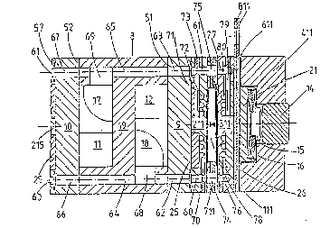
Two bor~ holes 60 and 61 runni~g in th~ direction of the
sandwich~like ass~mbly are disposed on each of th~ upper and
lower ~dge~ of the i~ner Qlectrod~ plate 211 shown in Fig. 4.
These bore holes 60 ~nd 61 are continued Vi& in ~ach case ~
drill hole 6~ and 63 aligned thereto in the dir~ction of thQ
middle bar 8 by me~ns of the plates 9 ~nd linkQd by in each cnse
ona bore hol~ 64 and 65 in the middl~ bQr 8 with the
corresponding bore holes 66 and 67 in thQ pl~te 10. Tha bore
hole 64 is linked to the cavity 12 ~nd the bore hol~ 65 is
connected with the c~vity 11 by mean~ of cut-outs 68 ~nd 69
r~specti~ly par~llel to the crosspiece 19.
The bor~ hols 61 is linked vi~ ~ furth~r bore hole 71 le~ding
radially Ero~ the edge of the inner electrode pl~te 211 through
~ lid 25 with the inner end of a cooling channel 72 formed by
groove having sever~l ~indings, for ex~mple spiral sh~pad
windings, lying in a plane parallel to the diode barrier
layer and the bore hole 60 is linked by a bore hole 70 with
the outer end of the same cooling channel 72. The
cooling channel 72 is covered by the lid 25 which terminates
with the inner electrode plate 211 to form a tight cooling
water system. The part of the bore hole 70 leading from
the outer edge of the inner electrods plate 211 to the
bore wall of the bore hole 60 and also the corresponding
part of the bore hole 71 are each provided with a plug 73.
~7~
w ~ ,7
- 10 -
The diameter of the resil ient intermediate plat~ 711 has, in
comparison to the bore holes 60 and 61 in the i~ner electrode
plate 211, e~panded bore holes 74 and 'J5 running in the
direction of the a~is thereof.
Bore holes 74 and 75 in the resilient intermediate plate 711 are
continued along the same axis direction in the outer electrode
plate 311 and end there in ~lind holes 76, 77 respectively.
From the blind hole 77 in the electrode plate 311 a bore hole 79
leads radially from the edge of tha elactrode plate 311
therethrough and a lid 26 leads to the inner end of a, for
example, spiral-shaped cooling channel 80 formed by a groove by
analogy with the cooling channel 71 in the electrode plate 211
and the lid 25.
Recesses are provided at the exits of the bore h~les 62, 63, 66,
67 ending at the surface facing a~ay from the middle bar 8 to
take up seal rings 57 which reliably seal the bore junctions.
Starting from connection 17 of the cooling medium inlet from a
heat exchanger or cold ~ater connection (not shown~ the
inflowing watar is distributed from the ca~ity 11 by means of
parallel cooling circulations to the individual diodes to be
: cooled and is led back to the heat exchanger or to a waste water
piping via the cavity 1~ ~nd its outlet 18. Th~ flon of uooling
,~
I
~3~i7~7
mediu~ to the individual diodes is again described using as
example the two diodes 111 and 115 arranged symmetric~lly to the
middle bar 8. The cooling water flows rom the cavity 11 into
the cut-out 69 and branches there into the bore hole 65 to the
right and to the diodes 111 and 115 to the left. The right path
laads via the bo~e holes 63, 61 and branches in the inner
electrode plate 211 via the bore holes 71 in the direction of
the cooling channel 72, cools the cathode of the diode 111
during its, for example, spiral path therethrough and then flows
through the bore holes 70, 60, 62, 64 and the cut-out 68 back
via the cavity 12 to the outl~t 18~ The other cooling water path
of the branch into the inner electrode plate 211 leads further
via the bore hole 61 to the bore hole 75, the blind hole 77 and
the bore hole 79 to the cooling water channel 80, cools the
anode of the diode 111 a$ this point and flows back via the hore
hole 78, the blind hole 76, the bore hole 74, joins up in the
bore hole 60 with the cooling water of the cathode and then
flows along the above described path to the outl~t 18. The left
path leads from the cut-out 69 via the bore holes 65, 67 to the
branch in the inner:electrod~ plate 215 whereby cathode and
anode of the diode 1~5 are cooled as described above and the
cooling water ~lows back through the bore holes 66, 64 and the
cut-out 68 to the cavity 12.
~'
~: :
~3~ 7
- 12 -
Other coolable electrical elements, for example resistances, can
be incorporated in place of the diodes 111 to 138 with
correspondingly adapted electrode plates 211 to 238 and 311 to
338.
It is, however, also possible to use in each case only one to
three semiconductor diodes instead of the in each case four
semiconductor diodes 111 to 138 for each phase half wave. It is
also possible to incorporate other electrical elements to be
cool~d, e.g. resistances with corre~pondingly adapted electrode
plates 211 to 238 and 311 to 338 in place of the diodes 111 to
138.
The three pha~e high-current transfo~mer 4 can also be replaced
by three single phas~ high-current transformers, the sQcondary
windings of which are connected on one side to the copper bar
101/102, 201/202 and 301/302 and to in each case one middle
tappin~ bar 13. In place of the three single pha~e high-current
transformers with secondary side middle tappings it is also
possible to use recti~ier circuits in bridge circuit, in which
case the middle bar 8 is absent and one or both plates of the
direct current c~nductor or one each o~ the cavities 11 or 12
tak~s up the cavities 11, 12 for inflowing or outflowing cool ing
water. Switch arrangements with few~r tha~ three phases are also
posslb1e.
.
.
- 13 -
The preferred material for assem~lies in which cooling water is
conducted is electrolyte copper. It has been found that,- unlike,
for example, aluminium, electrolyte copper shows no or only
slight corrosion when tap water is used as the cooling medium.
It was surprisingly ~ound in the context of tha invention that
normal (electrically conductive) tap water can be used AS
cooling ~aterial. This is baOE~d on the finding that the
potential differences hetween the individual assembles
electrically insulat~d by insulation material 51, 52, 711, 712,
..., but traversed by the same cooling madium flow ~re minimal.
Electrochemical material erosion is reliably ~voided by using
copper and copper alloys for all the conductors comin~ into
contact with the ~ooling fluid, but would, for example, occur in
the case of alumlnium. Instead of normal tap water it is of
course also possible to use poorly conducting or insulating
cooling fluids such as deionized water or oil.
The cooling water inlets an~ ou~lets 17 and 18 are adapted to
the lower front end of the middle bar 8, but c~n also be
provided on the upper face end of the middle har 8 without
. ~
impairing the mode of operation.
In the case of plates 9, 10, 211 and 215, ... consisting o~
aleatrolyte copper, i.e. of a soft material, thQ sQal rings 57
may be dispensed with and the surfaces o~ the plates 9 and 10
~ '
.
.
,' ' ~ ~ '-
, ' : ' ' . '
577~
- 14 -
and/or the surfacas of the adjacent plates 211 and 215, O.. can
: be roughened with ridges so that they f~rm a saal when
subsequently assembled by tiyhtening the screws 20 between the
pressure plates 411, 412, ... and the middle bar 8.