Note: Descriptions are shown in the official language in which they were submitted.
~q,.l"~
1. Field of the Invention.
The present invention relates to the field of computer
memory management units, and more specifically, to mapping less
than 32 bits onto a 32-bit memory address bus.
2. Prlor Art.
In most computers, a central processing unit (CPU)
communicates directly with both an address bus and a data bus.
These buses are coupled to a memory system in addition to
numerou~ other items, such as input/output ports, specialized
processors, DMA units, etc. The new generation of
microcomputers of today utilized single chip CPUs such as the
8086, 80386, 68000 and 68020. More recent chips, such as the
80386 and the 68020 utilize 32 bit address signals to access
variou locations within the memory.
Memory management units are well-known in the prior art and
are used to provide efficient utilization of the computer's main
memory. These units perform housekeeping functions, such as
remapping, and often include a memory which stores data
containing relocation of an address base and providing paging
functions. Because of the complexity of present day CPU chips,
more complex memory management units are provided to perform
extensive and complicated memory management functions. One such
chip is the 68851 paged memory management unit by Motorola Inc.
to support the 68020 chip.
However, until the advent of the 32-bit microprocessor
chips the earlier CPUs operated on 16-bit and 2~-bit addressing
schemes. Considerable software, including operating systems,
~ 5~
1 have been written to run on the~e prior art 16-blt and 24-bit
computers. Prior art memory management units operating ln
conjuction with these earlier CPUs are not able to provide the
extended addressing bit capability of the new 32-bit processors.
Although 32-bit memory management units are available, such as
the aforementioned 68851, such units are very complex, costly
and provide significantly more complex functions than the basic
memory remapping which is required to convert the prior art
16-bit and 24-bit address ranges into a 32-bit address map.
For example, the MacintoshTM computer sold by Apple
Computer Inc. of Cupertino, California, provided a 24-bit
address scheme, wherein 24 bits physically addressed the memory.
A newer computer operating on the 68020 CPU is now capable of
addressing considerable more memory space due to its 32-bit
lS address configuration. However, to run the earlier software
written for the 24-bit machine, the 32-bit system must be
capable of converting the 24-bit address range of the older
system to a 32-bit address range of the newer computer system.
Although other memory management units are capable of performing
this function, the memory remapping of 24 to 32 bits can be
accomplished much more simply and economically with the present
invention.
The present invention builds upon those prior art memory
management units, as well as the more recent 32-bit memory
management units. The memory mapping unit of the present
invention is simplistic in design and function and is economical
from a cost stand point. The memory mapping unit of the present
invention is capable of providing a 32-bit address range to
physically access the memory by using the more recent 32-bit
l~S ~.~`l) .~
1 addressing scheme, or alternatlvely, converting the prior art
address scheme having less than 32 bits to a 32-bit address.
J
1 S~ aY_QE_I~E T NYFNTIQ~
The present invention describes an apparatus for permitting
a 32 address bit CPU and main memory to run 24 address bit
programs. A memory mapping unit (MMU) of the present invention
is placed between the CPU and the main memory Whenever the CPU
runs programs designed to generate 32-bit addresses for
accessing main memory, the MMU permits the address signal to
pas4 without remapping. However, whenever the CPU runs programs
designed to generate 24-bit addresses, the MMU converts the 24
bits and provides a 32-bit physical address signal. The
remapping is essential because equivalent tasks of each program
need to access equivalent areas of memory.
The MMU as implemented in the preferred embodiment
processes the four most significant bits of the 24-bit address
signal and generates the twelve most significant bits of the 32-
bit physical address signal. Further, the processing is
achieved using comb~natorial logic implemented in gate-array
technology.
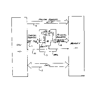
Figure 1 ls a block digram showing the various disposition
of address signals processed by the memory mapping unit of the
present invention.
Figure 2a is a schematic diagram showing the upper left
quadrant of a mapping circuit of the preferred embodiment.
Figure 2b shows-the upper right quadrant of the mapping
circuit.
Figure 2c shows the lower left quadrant of the mapping
circuit.
Figure 2d shows the lower right quadrant of the mapping
circuit.
3 ,~6 ~
ION
A memory mapping unit ls described for use in a digital
computer which includes a central processing unit (CPU) and a
main memory. In the following description, numerous specific
details are set forth such as specific memory sizes, part
numbers, circuits, etc., in order to provide a thorough
understanding of the present invention. ~owever, it will be
obvious to one skilled in the art that the present invention may
be practiced without these specific details. In other
instances, well-known structures and circuits are not described
in detail in order not to unnecessarily obscure the present
invention.
Referring to Figure 1, the memory mapping scheme of the
present invention is shown. A CPU 10 is coupled to access
memory 11. A data bus 12 couples the data between CPU 10 and
memory 11. The memory 11 is arranged such that it is mapped by
a 32-bit address signal from CPU 10. The memory mapping unit
(MMU) 15 of the present invention is located to accept logical
address signals from CPU 10 and to provide physical address
signals to memory 11. The CPU 10 of the preferred embodiment is
a Motorola 68020 CPU chip which provides a 32-bit address
signals. The eight lower significant bits (LSBs) are passed
directly to memory 11 on address bus 16 to provide the 8 LSss
for the physical address signal. The other 24 bits are provided
from the CPU 10 as logical address on logical address bus 17.
Bus 17 is coupled to MMU i5, wherein the 24 address bits,
LA8-LA31, are split into two paths. Bits LA8-LA19 are directly
coupled to provide physical address bits A8-Al9 on physical
~ .~5 ~ &(~:~
l address bus 18. Bits LAl~-LA31 are coupled to mapplng circuit
20, wherein circuit 20 provides the 12 most significant bits
(MSBs) A20-A31 of the physical address signal on bus 18.
Although bus 16 and 18 are shown as two separate ~uses in Figure
1, in actuality buses 16 and 18 comprise a single 32-bit
physical address bus for accessing memory 11. Various other
lines are coupled between CPU 10, MMU 15 and memory 11, and are
shown by a single line 22 in Figure 1 for the purpose of
simplicity. Clocking signals, function code signals, bus
acknowledge signals, strobing signals and other control signals
are included as part of line 22.
In operatlon the lower order 8 bits, A0-A7, are coupled to
memory ll without transitioning through MMU 15. The other 24
address bits from CPU 10 are coupled to MMU 15 on bus 17.
Physical address bus 18 provides address bits A8-A31, which when
combined with address signals A0-A7-provide the 32 bits needed
to access memory 11. When CPU 10 is processing software which
was written to provide 32 bits of addressing, circuit 20 will
accept LA20-LA31 and pass the 12 bits through to provide address
bits A20-A31. Therefore, in the 32-bit mode all 32 bits from
the CPU 10, A0-A7 and LA8-LA31, are coupled straight through to
memory 11 as physical address signals A0-A31 permitting the CPU
10 to provide the physical address of memory 11.
When executlng earller Maclnto~hTM computer software, only
the 24 LSBs of the 32-bit address field emanating from CPU 10
contain useful information. The 8 MSBs, LA24-LA31, are not
relevant to the address field, and hence, are ignored by the MMU
15. The 8 LSBs are generated directly onto bus 16 as address
signals A0-A7. The other meaningful address bits, LA8-LA23 are
I~f'~
1 inp~t~ed lnto ~MU 15. ~MU ~5 pa8ses LA8-~Al9 dlrectly as before
to b~ 18 a8 A8-Al9. The MS~3 of the 24-blt sddress, LA20-LA23,
are rem~pped by circuit 20 to provide the 12 phy3ical addre~s
signal~ A20-A31, ~herefore, ln the 24~ mode, the lower 20
address bitS a~e passed di~ectly through to memory 11 as ~ddress
siqn~l~ AO-A19 and the upper 12 b~t from CPU 10 are converted
and remappe~ by circult 20 to pro~lde address 8~ gnals A20-A31.
The mapp~ng ~cheme o~ mapping a 24~bit addre~s r~nge to a
32-~lt addregs xanqe to acces~ memory 11 a~ ~qed in the
preferre~ e~bodiment i~ shown below:
2g~t addr~ ra~ ~ hl~ addre~s ra~4~
$xxOO 0000 $xx7F FFFF $0000 0000 $~07F FFFF
~xx80 0000 $x~F FFFF $4000 0000 $400F FFFF
$xx30 0000 $~x9F FFFF $F9o~ 0000 SF9OF FFFF
$xx~0 0000 $xxAF FFFF $FAOO 0000 $FAOF FFFF
$xx~0 0000 $xxBF FFFF $FB00 0000 $FBOF FFFF
$xxCO 0000 $xxCF FFFF SFCOO 0000 $FCOF FFFF
$xxD0 0000 $xxDF FFF~ $FDOO 0000 SFDoF FFFF
$xx~0 0000 $xx~F FFFF $FEOO 0000 SF~OF FFFF
SxxFO 000~ $xxFF FFFF $5000 0000 S500F FEFF
~ble 1
~he addre8se8 ~e 8hown daplcted in hexide~al code, .~uch
that each di~it iB xepresented ~y 4 ~ddr~ss blts. For sxample,
~ 24-blt ~ddre~8 of $90 0000 1~ converted by ~he M~N 15 to a 32-
blt addre~g $F900 0000. It sho~ld be noted that in th~
remapplng schsme thè lower f~.ve dlgltg, which determlne addres~
B
l bits A0-A19 are never changed when remapped to the 32-bit
address range. Only the most significant digit ~the 4 MSBs) of
the 24-bit addre~s is converted to provide bits A20-A31, when
remapped to the 32-bit physical address. For example, a 2g-bit
address of SBo 0000 is converted to a 32-bit address by
remapping the digit B to provide the three most significant
digits FB0 of the 32-bit address. For an address of $BF FFFF,
the digit B is still remapped to digits FBO to provide a
physical address of $FBOF FFFF. An address between $B0 0000 and
$BF FFFF is remapped linearly between $FB00 0000 and $FBOF FFFF.
The other address ranges are remapped equivalently. In
functional terms, circuit 20 when in the 24-bit mode will take
the most significant digit of the 24 bit address, LA20-LA23, and
generate a new three digit, 12 MSBs, of the 32-bit physical
address.
Referring again to Table 1, the remapping scheme of
remapping the 24-bit physical address space of the earlier 24-
bit software into a 32-bit physical address space is arbitrary
and is left to the designer. However, the remapping scheme of
the preferred embodiment as shown in Table 1 is designed
specifically, such that portions of the memory allotted to a
particular task in the earlier version of the MacintoshT~
computer is mapped to an equivalent memory space in the memory
of the newer computer system using the 32-bit memory address.
Obviously, because of the size of memory 11, there will be
excess memory space when the 24-bit physical address space is
mapped into memory 11. Although a particular addressing scheme
using a 24-bit to a 32-bit conversion is described, ~t is
appreciated that other remapping address schemes, including
3 ~ o~
1 converslon of other than 24 bits, can be practiced without
departing from the spirit and scope of the invention.
Referring to Figures 2a-d, a circuit schematic of circuit
20 of Figure 1 is shown. Various logical address signals LA14-
LA31, as well as various control signals, are shown as inputs to
input buffers 31. The upper signals LA14-LA19, R/W, FC0-FC2,
LASr and clocking signal C16M are utilized to develop PAS and
BER~ signals, and are not pertinent to the address conversion
provided by the MMU 15. The actual address translation is
provided by a portlon of the circuit associated with input
signals LA20-LA31 and function code signal FC3.
The BGACK is a bus acknowledge signal, which is not
actually used for ramapping, but is necessary for activating
output buffers 60 and 101. A 68020 users manual can be
consulted for a precise purpose of the various CPU signals
described above. The 24 or the 32-bit mode of the circuit 20 is
controlled by the state of signal FC3. Whenver FC3 is low, the
MMU 15 operates to transfer the 32 bits from the CPU straight
through as physical address to memory 11. Whenever FC3 is high,
MMU 15 is in its 24 bit mode and signals LA20-LA23 representing
the MSBs of a 24-bit address signal is used to provide a
remapped 32-bit address ~ignal.
When in the 32-bit model signals LA24-LA31 are coupled to
NAND gat~s 41-48, which outputs are coupled to NAND gates 51-58.
2S The outputs of NAND gates 51-58 are each coupled to its
~ respective tristate output buffers 60. When in the 32-bit mode,
FC3 is high, placing a high on second input of each of NAND
gates 91-48 such that the outputs of gates 41-48 will be
determined by the state of the signals LA24-LA31. FC3 siqnal is
L
l inverted by lnverter 71, which output is coupled to an input of
various NAND gates 81-91. The output of NAND gates 81-91 are
coupled to various input of NAND gates 51-58 and 65-~7 as shown
in the schematic. Signals LA23-LA20 are coupled through buffer
73 to AND gate 64 and NAND gates 61-63, respectively. In the
32-bit mode, signals LA20-LA31 are coupled through dual NAND
gate configuration, such as NAND gates 41 and 51, or through a
single AND gate, such as for LA23, wherein t~e state of the
signals LA20-LA31 are unchanged as they are outputted as A20-
A31.
The outputs of gates 51-58 and 64-67 are each passed
through its respective tristate output buffer 60 to provide
address signals A20-A31. Buffers 60 have their tristate enable
line coupled to BGACK signal through inverter 75. As long as
signal BGACK remains high, tristate buffers 60 are enabled to
provide an output. However, when BGACK goes low the tristate
buffers 60 are placed in its trlstate position and circuit 20 is
decoupled from provlding address signals on lines A20-A31.
When operating in the 24-bit mode, function code FC3 goes
low and a low state is placed on the input of gates 91-48 and
61-64, such that the output of these gates 41-48 and 61-63
remains high and the output of gate 64 remains low causing LA20-
LA31 from transitioning to the output A20-A31. Therefore,
signals on LA24-LA31 are basically decoupled from passing
through circuit 20, due to the operation of gates 41-q8 and 61-
64. In the 24-bit mode, where bits 24-31 represented by LA29-
LA31 are non-functional bits, they are excluded from the
operation of the circuit 20.
0 1
1 Signals LA20-LA23, which represent the most significant
digit of a 24-blt address and which provide the remapping in the
preferred embodiment, are used for the necessary decoding to
generate remapped signals A20~~31. Buffer 73s and inverters 74
couple signals LA20-LA23 to corresponding NAND gates 81-91 as
shown on the schematic to provide the necessary decoding for the
address translation. FC3 is low in this instance such that the
output of inverter 71 is at a high state, permitting gates 81-91
to respond to various inputs coupling signals LA20-~A23.
Outputs of gates 81-91 are coupled to NAND gates 51-58 and 65-
67, wherein further address translation is provided in gates 51-
58 such that LA20-LA23 of a 24-bit addres~ signal is converted
to provide A20-A31 of a 32-bit physical address signal to
address memory 11 of Figure 1.
It should be pointed out that a single AND gate 64 is used
for the generation of address signal A23 in the preferred
embodiment, because address sign~l A23 will be 0 whenever
converting 24 bitQ to 32 bits. This is done in the preferred
embodiment because, as can be seen in Table 1, the largest value
~ encountered by the sixth digit during the remapping is a value
of 7. However, address line A23 could be implemented using two
NAND gates and appropriate decoding as is the case with the
other address signals. Therefore, in the 24-bit mode, input
lines LA24-LA31 are disregarded and signals LA20-LA23 are used
to provide the decoding for generating the most significant 12
bits A20-A31 by gates 81-91, 51-58 and 64-67.
The remaining portion of circuit 20 is not required for the
remapping described above, but does take advantage of the 32-bit
line from the CPU 10 to provide certain user functions. The
12
Jl) L
1 twelve input address signals LA20-LA31, as well as address
signals LA14-LAl9, are coupled through various NOR gates 92 and
the output of NOR gates 92 are coupled to a five input NAND gate
93, such that only when all inputs LA14-LA31 are low the output
of NAND gate 93 will be low. The output of NAND gate 93 is
coupled to an input of NOR gate 94 along with FC2, LAS and R/W
signals, such that whenever signals LA14-LA31 are all low, FC3
is in user mode (low state) and a write is attempted, a bus
error signal BERR will result at the output of buffer 95.
Flip-flop 96 is a D-type flip-flop coupling the output of
NOR gate 94 to buffer 95. Output of NOR gate 94 is coupled
through inverter 96 to an input of NAND gate 97, which also has
its input an inverted LA~ signal (LAS), as well as a combination
of FCO-FC2 coupled through NAND gate 98. Gate 97 provides an
lS output to a J input of a J-K flip-flop 99. The Q output of J-K
flip-flop 99 is coupled through inverter 100 and then through
buffer 101 to provide a PAS signal. Buffer 101 is a tristate
buffer, wherein the enable line is coupled to the same enable
line as buffers 60. Output of NAND gate 97 sets the J-K flip-
flop 99 and provides a low on the Q output of the flop-flop 99.
The output of ~AND gate 97 is also coupled to the K input of
flip-flop 99 through inverter 102 to reset flip-flop 99. Clock
signal C16M is coupled to clock inputs of flip-flop 99 and 96
for sychronizing these two flip-flops. The purpose of flip-flop
99 is to simply convert the LAS signal to a PAS signal at the
output of buffer 101.
As stated earlier the upper portlon of circuit 20 is
nonmaterial to the operation of the address translation of
converting 24-bit address space into a 32-bit address space.
~`~q~
l Further, circuit 20 of the preferred embodiment is structured
using known gate array techniques, such that circuit 20 is
embodied in a single semiconductor chip. However, other
configurations and techniques, not necessarily gate arrays, can
be used to provide the address translation of the present
invention without departing from the spirit and scope of the
present invention. Also, circuit 20 shows other components,
such as pull-up resistors associated with buffers 31, unused
inverters ~shown within the dotted lines associated with gates,
such as gate 51), and pads for coupling various signals to and
from the chip, but these features are well-known in the art and
do not add to the teaching of the present invention.
Thus, a memory mapping unit for a computer is described.
14
.;
~ ,