Note: Descriptions are shown in the official language in which they were submitted.
~3~
MAGNETORESISTIVE MAGNETIC SENSOR
BACKGROUND OF THE INVENTION
The present invention relates to magnetic
field sensors based on magnetoresistive material and,
05 more particularly, to such sensors requiring low
usage of electrical power.
There are many situations in which there is
a need to measure a magnetic field. Among such
situations are the measurement of position or
proximity of a magnetized portion of a structure, the
readout of stored magnetic information, the
measurement of current flows without the need of a
measuring device in the current flow path, etc.
Many of the magnetic effects in such
situations are relatively small and therefore require
a sensitive magnetic sensor. A magnetic sensor
capable of sensing such small magnetic field
perturbations, and which is economical to fabricate,
is provided on the basis of the magnetoresistive
effect. Such magnetoresistive material based
magnetic sensors can be fabricated using monolithic
integrated circuit fabrication techniques, and so can
not only be made economically but also made quite
small in size. The magnetoresistive material is
provided as a thin film when fabricated using
monolithic integrated circuit techniques.
A magnetoresistive material based magnetic
sensor is arranged by providing a maqnetoresistive
material to be used as an electrical resistor. A
current is passed therethrough, and the voltage
thereacross will depend on the effective resistance
of the material over the path in which the current
flows. That resistance value will depend in turn on
~3r~0~
the state of the magnetization of the material. If
the magnetization is parallel to the current flow,
the material will exhibit a maximum resistance, and
it will exhibit a minimum resistance for
05 magnetization perpendicular to the current ~low.
In the magnetoresi~tive material there will
be an effective magnetization, and this will be
directed primarily along the easy axis of the
material. An external field acting on the magneto~
resistive material will rotate the magnetization
direction therein to change the resistance of that
material as a result. The changed resistance
carrying the current causes a voltage drop change
across the resistor which can be sensed as an
indication of the magnitude of the external field.
The effective resistance of such a film will
vary as the square of the cosine of the angle between
the effective magnetization direction and the current
flow direction through the material. The total
resistance, however, is usually not of interest but
rather the change in resistance in response to a
change in the applied external magnetic field. This
change is o~ten best measured at a point along the
squared cosine response curve where the curve
approximates a linear function.
To provide operation on such a linear
portion of the response curve requires that there be
an initial angle between the direction of current
flow and the nominal direction of magnetization in
the absence of any externally applied fields~ This
can be accomplished in alternative ways in a bias
arrangementO The magnetoresistive material can be
placed on the device substrate as a continuous
resistor in a "herringbone" pattern or set of
continuously connected multiple inclines, wi~h the
angle of incline being approximately 45 with respect
to the direction of extension of the resistor. There
05 then must be provided a source ~or a magnetic bias
field to be pointed in a direction which is 90 to
the direction of the extension of the resistor.
Another method is to provide a linear strip
of magnetoresistive material, but to add individual
conductors across that strip at an angle of 45 with
respect to the direction of the strip. This, in
effect, causes the current to flow at an angle
through the magnetoresistive strip with respect to
the direction of elongation of the strip itseLf.
This latter configuration is often called a "barber
pole" sensor because of its configuration, and such
an arrangement can eliminate the need for an external
source of a magnetic bias field~
For low power usage, such a "barber pole"
sensor is most eff~ctive if the magnetoresistive
material strip is very long with respect to its
width. This increases the resistance of the
magnetoresistive material strip between its ends to
thereby lower the power required to operate the
device, and further, it substantially reduces
demagnetization effects within the magnetoresistive
material strip. However, there are limits to the
length that such a strip can be continuously provided
in a monolithic integrated circuit chip, and so the
strip is often folded into a series of parallel
portions. ~ach portion, as a series link, then folds
back ~ith respect to the preceding series link to
thereby foxm a much more compact ma~netoresistive
material structure.
s~
This leads to a relatively sharp curvature,
however, at the locations where the magnetoresistive
material in the folded strip completes one series
link portion and then is bent: around 180 to continue
05 in a direction parallel to the precedin~ link to form
another. These sharp turn regions lead to the
formation of so-called magnetic end-domains in and
near these bend regions. The magnetization direction
in such domains can vary substantially with respect
to the direction of magnetization in the parallel
portions of the continuous strip. The magnetization
of the parallel portions themselves will be well
aligned with the direction of extension of each
portion because of the length compared to the width
thereof leading to reduced demagnetization effects
therein.
A particular difficulty with such end-domains
is that they are susceptible to change with
temperature and external magnetic field excursions,
and so does the magnetization direction therein.
This has the effect of causing random fluctuations in
the resistance of the strip and so in the voltage
value occurring across the magnetoresistive material
sensor for a given current therethrough. If four
such magnetoresistive material sensors are used in a
bridge circuit, these voltage variations due to
thermal changes in the end-domains will lead to
randoml~ changing values or fluctuations in the
voltage of the bridge between the sense connections
leading to errors in measurements based on a
magnetometer using such a bridge. Thus, there is a
desire to provide a magnetoresistive magnetic sensor
having a more stable voltage occurring across the
o~
64159-1097
magnetoresistors therein despite temperature excuræions.
~UM~ARY O~ T~ INYE~TION
The present invention provides a magnetoresistive device
having a plurality of magnetoresis~ive material strips, there
being a first conductor positioned over the strips near the first
end of each but isolated from such strips, and a second conductor
positioned over such stripæ near the second ends thereof but again
being isolated from the strips. The strips are connected together
to pass current therethrough. This connection can be made at the
ends thereof for strips that are parallel to one another 50 that
the strips are electrically connected in series. These ends may
be tapered outslde of the conductors. More than one of these
arrangements can be connected toge~her to form a sensing circuit
including forming a bridge circuit.
According to a broad aspect of the invention there is
provided a magnetoresistive device for sensing magnetic fields,
said magnetoreslskive device having iirst and second power
terminal regions, said device comprising:
a first plurality of magnetoresistive material strips
provided on a substrate each having a first end and a second end
by which it is connected to pass electrical current if provided at
said first power terminal region;
a first conductor electrically connected to a first terminal
means adapted for connection to a first source of current, said
first conductor positioned over each of said first plurality of
magnetoresistive material strips near said first end thereof but
lsolated therefrom; and
~L3`~6~
5a 64159-1097
a second conductor electrically connected to a second
terminal means adapted for connection to a second source of
current, said second conductor positioned over each of said first
plurality of magnetoresistive material strips near said second end
thereof hut isolated therefrom.
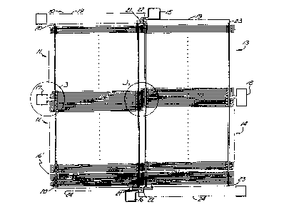
BRIEF DESCRIPTION OF THE DRA~INGS
Figure 1 shows in part a layout dlagram of an embodiment
of the present lnvention,
Figure 2 shows a cross section view of a portion of the
present invention, and
Figure 3 shows fragment views from Figure 1.
DETAILE~ DESCRIPTIO~ OF THE PREEERRED EHBODIMENTS
Figure 1 shows a monolithic integrated circuit layout
diagram for a "barber pole" magnetic field sensor, 10, based on
four arrays, 11, 12, 13 and 14, of magnetoreslstive material
strips. Each of arrays 11, 12, 13 and 14 have a set of parallel
positioned magnetoresistive strips electrically connected in
series with one another which will be described in more detail
below. The dots within each
r~
~o~
~ 6
array indicate that only some of the strips are
shown. ~ot all of the layers are shown, and some
hidden lines are suppressed for clarity.
Arrays 11 and 13 are electrically connected
05 together by an associated interconnection arrangement
electrically connected also to a power supply
terminal pad, 15. Arrays 12 and 14 are electrically
connected together by another associated
interconnection arrangement electrically connected
also to a power supply terminal pad, 16. The
interconnection arrangement associated with power
supply terminal pad 16 involves a resistance value
balancing arrangement, 16', formed of the same
magnetoresistive material. Arrays 11 and 12 are
electrically connected together through an associated
interconnection arrangement electrically connected
also to a sense signal output terminal pad, 17.
Arrays 13 and 14 are electrically connected together
by an associated interconnection arrangement
-electrically connected also to a sense output
terminal pad, 18. Alternatively, terminal pads 17
and 18 could ju~t as well be for a power supply with
terminal pads 15 and 16 being sense signal outputs.
Sensor 10 of Yigure 1 has a further
interconnection arrangement to provide supplementary
magnetizing fields near the ends of the
magnetoresistive material strips in each array. A
first current supply terminal pad and current
distribution arrangement, 1~, distributes current
with respect to four conductors to provide four
current paths, 20, 21, 22 and 23, being electrically
joined thereto. A further current supply terminal
pad and current distribution arrangement, 24, is
-- 7 --
provided at the other end of these four conductors
and is electrically joined thereto.
Figure 2 shows the general construction of
the monolithic integrated circuit involved in the
05 layout of Figure 1, though not to scale and not
necessarily in proportion for purposes of clarity.
This monolithic integrated circuit is fabricated
based on a semiconductor material substrate, 30,
typically of silicon doped in the manner necessary to
support other circuit portions of the monolithic
integrated circuit. Substrate 30 has an insulating
layer, 31, typically of oxides of silicon, primarily
silicon dioxide. The thickness of layer 31 is
typically l.O~m. A further insulating layer, 32, is
provided thereon and is typically a silicon nitrida
of a thickness of 0.5~m. Layer 32 provides a
suitable surface on which to provide the
magnetoresistive material.
The magnetoresistive material forming a thin
layex, 33, on layer 32 is typically a ferromagnetic
thin film having a thickness of 200 A and formed of
an alloy composed of nickel, cobalt and iron. As one
example, the film material might comprise
appro~imately 81% nickel and 9% of iron. In some
situations, other materals are added to the alloy in
relatively small amounts to improve selected
properties of the film. The suggested composition
will lead to there being relatively little
magnetostriction occurring in the film, but there
will be significant magnetoresistance and the ~ilm
will exhibit uniaxial anisotropy.
The films may be annealed at an elevated
temperature for several hours in the presence of a
~3~ g
substantial magnetic field applied in a direction
coincident with the axis of elongation of the
magnetoresistive thin film strips to improve film
stability. This occurs through increases in grain
05 sizes and improving the coincidence of the material
easy axis with the shape induced easy axis to reduce
magnetic dispersion.
A film of tantalum nitride, 34, of a
thickness of only 150 A is provided over the
magnetoresistive material. Such a film will be
conductive vertically in Figure 2, but will be highly
resistive laterally because of its thinness and the
material properties. Thus, the provision of a series
of conductive straps, 35, to impart current
directionality in magnetoresistive layer 33, at an
angle of 45 to the direction of elongation of the
magnetoresistive material strips on the surface of
layer 34 leaves these straps (i) in electrical
contact with magnetoresistive material layer 33, but
(ii) effectively electrically isolated from one
another because of the properties of layer 34.
Straps 35 have a thickness of approximately 0.5~m and
are formed of aluminum alloyed with approximately 4%
copper. The sideways extension of straps 35 due to
their angular placement is omitted from ~igure 2 for
clarity.
This set of aluminum straps is covered with~
and the separations therebetween were filled, by a
further insulati~g layer, 36, of typically silicon
nitride extending approximately l.O~m above the
surface of tantalum nitride layer 34. L~yer 36
protects the surface of the aluminum straps and
provides an insulating barrier between them and the
next layer above.
This next layer, 37, on nitride layer 36 is
typically a further layer of aluminum alloyed with 4%
copper, and is used to provide conductors 20, 21, 22
and 23. Layer 37 is provided typically in a
05 thickness of l.O~m. Layer 37 is covered with a
further insulating and protecting layer, 38, again
typically of silicon nitride to a thickness of
0.5~m. Interconnection terminal pads can be formed
thereon, again with aluminum alloyed with 4% copper
for interconnection purposes as desired. Such pads
have not been shown in the structure of Figure 2.
The formation of silicon wafer 30, in
providing the variously doped regions therein
necessary for other circuit portions, is done by
methods well known in semiconductor device
fabrication. Similarly, the provisions of the
various layers, and straps 35, generally all the
structures above silicon substrate 30, are also
fabricated using well known monolithic integrated
circuit fabrication techniques.
Arrays 11, 12, 13 and 14 of Figure 1 each
form a separate magnetoresistor comprising, as
indicated above, many series-connected
magnetoresistive strips. As such, and interconnected
as described above by the interconnection
arrangements associated with terminals 15, 16, 17 and~
18, these resistors form a four element bridge
circuit in Figure 1. In operation, current can be
supplied to terminal 15 and out at terminal 16, or
vice versa. The signal voltage is taken
differentially between terminals 17 and 18.
To balance the bridge output signal to as
near zero as possible in the absence of an external
~3~ 39
-- 10 --
magnetic field, resistive portions in balancing
arrangement 16' are usedO A substantial number of
long resistors are provided in arrangement 16' which
can be broken as necessary to equalize the resistance
05 between the two alternative current paths between
interconnection pads 15 and 16. The resistors in
arrangement 16' are formed of the same
magnetoresistive material as the strips aboved used
for sensing, but with a narro~wer dimension.
The resistances in arrangement 16' primarily
to the left of pad 16 are connected in parallel with
each other, and this group is connected in series
with arrays 11 and 12~ The slanting interconnection
line from upper left to lower right of these
resistors excludes the portions thereof to the left
to give several differing resistance values in
parallel to permit accurate balancing. The
resistances to the right of pad 16 in arrangement 16'
are connected in parallel, and this parallel group is
connected in series with arrays 13 and 14. The
slanting interconnection arrangement is used here
also. Breaking selected resistance tracks in either
increase~ the resistance in that leg of the bridge
circuit containing the arrays associated therewith.
The magnetoresistive material strips of
Figure 1 are shown in more detail in Figure 3, these
fragment Yiews being taken from the portions of the
sensor with the circles marked 3 in Figure 1. One of
these sections involves the interconnection
arrangement associated with sense signal terminal pad
17 and that terminal pad. This is shown in the
fragment view on the left in Figure 3 where it
extends to and contacts two magnetic material strips,
11' and 12', one from array 11 and one from array 12,
and each on either side of the space separating these
two arrays from one another. That is, this is the
point where these two arrays are joined in series
05 with one another by the interconnection arrangement
shown.
In addition to this interconnection,
magnetorssistive material strips 11' of array 11 are
each connected in series with one another as
indicated above. This is also true for the
magnetoresistive material strips in array 12, and in
arrays 13 and 14. The interconnections on the left
for magnetoresistive material strips 11' in array 11,
and for strips 12' in array 12, are formed by the
copper alloyed aluminum interconnections, 40. In the
left-hand portion in Figure 3, interconnections 40
are shown across the two magnetoresi~tive material
strips 11' and 12' connected together by the
interconnection arrangement associated with sense
signal terminal pad 17, and then successive pairs of
strips in each direction therefrom are connected
together by an interconnection 40.
The right end portions of magnetoresistive
material strips 11' and 12' are shown in part in the
~5 right-hand fragment view of Figure 3 where further
alloyed aluminum interconnections, 41, are provided
joining pairs of strips. The two magnetoxesistive
material strips 11' and 12' connected together by the
interconnection arrangement associated with sense
signal terminal pad 17, as well as by interconnection
40, are left apart and not connected together in the
right~hand view of Figure 3. Rather, each is
connected to the magnetoresistive material strip in
~3~ 9
- 12 -
its own array next adjacent thereto. Again,
thereafter successive pairs of these magnetoresistive
material strips in each array are connected together
by interconnections 41. Thus, the magnetoresistive
05 material strips in each array can be seen in the two
fragmentary views of Figure 3 to be connected in
series with one another. Further interconnections,
42, are shown interconnecting the ends of
magnetoresistive material strips 13' and 14' of
arrays 13 and 14, respectively, in the right-hand
fragment view of Figure 3.
This interconnecting of all of the many
magnetoresistive material strips in each array into a
single resistor comprising a long series o
interconnected strips as multiple links in the
resistor is done, as indicated above, to provide a
large resistance value for that resistor. This
increase in resistance leads to much lower power
drain when operating the sensor. The use of
interconnections 40, 41 and 42 avoids having any
bends in the magnetoresistive material which can lead
to end-domains. However, terminated strips are
subject to having so-called "buckling" magnetic
domains form at the terminated ends thereo~.
Buckling domains axe also a source of difficulty
through having the magnetization therein again being
susceptible to changing due to temperature and
external magnetic f ield changes.
Conductive straps 35 are shown in Figure 3
at 45 with respect to the direction of elongation,
or the direction of ext~nsion, of the
magnetoresistive material strips 11', 12', 13' and
14' shown there. Straps 35 have a positive slope for
~3~6~
the magnetoresistive strips of arrays 11 and 14, and
a negative slope for arrays 12 and 13. This results
in an external magnetic field, applied to the sensor
10, tending to cause an increase in resistance in two
05 of the arrays and a decrease in the resistance o~ the
other two. As a result, the bridge will become
unbalanced in resistance values in the t~o legs
thereof between terminal pads 15 and 16, and, for a
current therethrough, sense signal terminal pads 17
and 18 will exhibit a voltage difference
representative of the strength of the external
magnetic field, and, to some degree of the direction
of that field.
The direction of the field will be sensed
with respect to the axes of the sensor, one of which
passes through signal terminal pads 17 and 18 and the
other approximately perpendicular thereto. This
directionality dependence occurs because the
magneti7ation of the magnetoresistive material strips
is primarily along the axis of elongation, or the
extension, of those strips. An external field is
most able to rotate that magnetization in those
strips i~ it is perpendicular thereto, but is unable
to rotate magnetization if it is parallel thereto.
Arrays for such a bridge circuit sensor
arrangement have been provided in the past formed as
a continuous magnetoresistive material strip.
However, as indicated above, the resulting sharp
bends lead to the formation of magnetic end-domains
in the magnetoresistive mAterial at the bends,
domains having a magneti7ation which can shift ~ith
temperature excursions or the like so as to lead to a
varying voltage di~ference between output signal
~3~ 9
terminal pads 17 and 18 in the absence of an
externally applied magnetic field.
The use of interconnections ~0, 41 and 42 in
Figure 3 to electrically interconnect adjacent
05 magnetoresistive material strips into a single series
resistor, as indicated above, helps to eliminate this
source of output variation by electrically
interconnecting adjacent magnetoresistive material
strips with a nonmagnetic interconnection material to
avoid having sharply curved magnetoresistive
material. There is a gain using these interconnections
through positioning these interconnections on the
magnetoresistive material strips before reaching the
ends of the strips. Thus, the interconnections are
made before the portions in the magnetoresistive
material strips are reached in which buckling domains
tend to occur anyway, even without the bends in the
magnetoresistive material which is near the ends
thereof. This positioning of the interconnections
40, 41 and 42 assures that the current flow through
the magnetoresistive material strips does not take
placa in the end portions subject to having buckling
domains formed therein to thereby avoid voltage
variations from this source.
At least this last result will be true if
the buckling domains occurring at the ends of the
magnetoresistive material strips are confined to
remaining closer to the end portions of the strips
than are the positions of the interconnections ~0, 41
and 42 with respect to the magnetoresistive material
strip ends to which they are adjacent. Two further
measures are taken in sensor 10 to assure that such
buckling domains stay toward the strip ends beycnd
~3~iO~9
- 15 -
the locations of the strip interconnection. The
first of these measures is to taper the ends of the
magnetoresistive material strips as shown in Figure
3. Such tapering has been shown to reduce the
05 formation of buckling domains compared to those
formed in strips with squared-off ends. The tapering
reduces the surface magnetic pole density and seems
to provide some volume poles in the material itself.
The tapering should occur over a distance which is
typically one to four times the width or more of a
magnetoresistive material strip which has a typical
width of 20.0~m.
The other measure is the provision of
conductors 20 and 21 on either side near the ends of
magnetoresistive material strips 11' and 12' in
arrays 11 and 12, respectively, and conductors 22 and
23 on either side near the ends of magnetoresistive
material strips 13' and 14' of arrays 13 and 14,
respectivelyO The current direction through these
conductors is such as to create a magnetic field
therebelow at the magnetoresistive material strips
~hich has a direction substan~ially paralleling the
direction of desired magnetization in those strips.
Thus, this additional ~ield tends to strengthen the
existing magnetization in each of the
magnetoresistive material strips and, in effect,
prevent the occurrance of domains forming therein
having a magnetization in the opposite direction to
that desired. For thi~ purpose, further conductors
could be pxovided over other parts of the interiox of
these magnetoresi~tive material strips.
In addition, the magnetic fields resulting
from current flow through thes~ conductors tends to
~3~16~
- 16 -
pin or lock the existing maynetization occurring in
the center of the strip into continuing to extend
thereunder. This provides, :in effect, a barrier to
bucXling domains or other magnetic instabilities,
05 present near the ends oE these strips, from
propagating inward toward the portions of the
magnetoresistive material strips being used in
providing the sensing for magnetic sen~or 10.
Conductors 20, 21, 22 and 23 are typically
l.O~m in thickness, as indicated above, and have a
width comparable or greater than the width of the
magnetoresistive material strips. Strips of these
dimensions can support a substantial current on the
order of 10.0 mA or above to provide a magnetic field
thereunder of three Oe or more without causing
electrical migration of the material in the
conductors themselves.
These measures lead to a substantially
improved stability of performance of the magnetic
sensor insofar as having a much more stable voltage
appear between output sensor pads 17 and 18 over
temperature excursions. This results in less
variation in the output signal over substantial
periods of ti~e and between tests separated by
substantial periods of time, and so leads to less
uncertainty in the value of the externally applied
field being measured.
Although the present invention has been
described with reference to preferred embodiment~,
workers skilled in the art will recognize that
changes may be made in form and detail without
departing from the spirit and scope of the inVentiQn.