Note: Descriptions are shown in the official language in which they were submitted.
`` ~306310
Application of Epstein et al
. .:
~ . ~
~` l o Background of the Invention
1.1 Field Or the Invention
-~ Thig invention relates to digital computers, and particularly to dig~tal
computers adapted for use in a distributed data processlng system compri~ing andsharing load among a plurality of indlvidual digital computers.
1.2 Des~riptlon Or the E'rlor Art
Digit~l computers in general are well known in the prlor art. Digital
computerR have been employed ln "distributed computing networks" in which a
plurality of computers are interconnected and are progra~med to cooperate on an
overall data processing task lnvolving a related body of data and a related body.7 Or tasks to be performed thereon, with some computer3 doing some Or the
~rocessing and then passing results or status information to other of the
computers which perform other Or the processlng.
~91
Using traditlonal general purpose computers in distributed computing
networks has required that each computer perform a portion Or the networking
runotlons (intercommunication, coordination, priority arbitration, etc.) in
addition to its direct data processing work. With such traditional computers, it
~, has generally been neces~any to interconnect them by means Or their input/output
1 buses so that each views the others as I/0 devices and i8 thus responsible for
r~, detailed contro} over all transmissions to and from them.
r ' .`
1.3 Su nary Or the IDventlon
~!
~ ~ .
j The computers of the present invention overcome the overhead-prone
i drawbacks Or the prior art by provlding an architecture in which additional
i -11- ,,
`l
1306.~0
Application Or Epstein et al
intelligence is provided at junction points Or the computer network, this
intelligence being surficient to perform the networking overhead functions.
bus is provided for data transrers between each computer' 3 CPU and an intelligent
I/0 controller; another bus is provided for memory transfers; another bus is
provided for interconnecting the computers; an intelligent bus controller is
provided to tranQfer from any to any Or the the three buses. Flow Or data and
status information around the network is thuQ expedlted, and the CP~ Or each
computer is rreed to devote its attention to direct data processing tasks. An
., .
intelligent controller i9 provided ahead Or the video RAMs to free the CPU Or
detailed bitmap manipulation in support Or graphic dislays.
;~1 It i9 thus a general ob~ect Or the present invention to provide improved
digital oomputers.
.'~
It is a particular ob~ect Or the present invention to provide digital
computers that may be interconnected to form a highly efricient distributed
computlng system.
Additlonal obJects and advantages will be apparent to one skilled in the
art, arter referrlng to the descrlptlon or the preferred embodiment and the
~, appended drawings.
Brle~ Descrlptlon or the Dra~lngs
~'~
For olarlty, the rigure numbers are based on the number Or the section
re~errlng to the rlgure. For example, rigures rirst rererred to in Section 1 are
numbered in the "100" series, figures rirst rererred to in Section 2 in the "200"
Qeries, and so on.
~ i .
Flgure numbers 1 - 100 are not used.
.
Figure 101 (prlor art) i3 a block diagram Or a typlcal prior art general purposecomputer employed ln a dlstributed computer network.
-12-
~ ~ 130fi3~0
~ Application Or Epsteln et al
:,
~ ~ Figure 102 is a block diagram of the computer of the present invention employed
; in a distributed computer network.
Figure 103 i8 a block diagram of CPU 101
Figure 104 iQ a block diagram of IOC 202
Figure 105 is a block diagram of MC~ 201
Flgure numbers 106 through 200 are not used.
,,
I Figures 201 through 235 pertain to MCU 201 and I-Bus 204:
.~, , .
Figure 201 depicts the flow of an even double-word 32 bit trangfer.
1 Figure 202 depicts the flow of an odd double-word 32 bit transfer.
l
-i- Figure 203 depicts the flow Or justified 16-bit transrers.
,. ..
"~! Figure 204 depicts the ~low the un~ustified 16-bit transfers.
~i Figure 205 depicts the flow of justified 8-bit transfers
~, Figure 206 depicts the flow of un~ustified 8-bit transfers.
~.j
~ Figure 207 depicts the flow Or a block transfer.
,:
Figure 208 show~ the logical organization of glob~1 memory.
Figure 209 shows the makeup of a control word.
Flgure 210 is an overview of bus arbitrat~on ti~ing.
Figures 211a-211e schematlcally depict the bus arbltration priority
' ~' scheme.
-13-
; .
~ 1306310
Appllcation Or Epstein et al
.~., '.:
Figure 212 is a schematlc diagram Or the bus arbitration priority wiring.
'.,, . . -
', Figure 213 depicts an example of bus priority arbitration.
,~' Figure 214 iR a timing dia~ram of bus priority arbitration.
Figure 215 depicts a data format.
j Figures 216 through 223 are timing charts pertaining to bus arbitration
and bus data transmission.
Figure 224 is a table of command encodings.
Figure 225 illui~trates the timing of the Bus Clock signal
Flgures 226 through-234 illustrate the timing of var~ous bus control
signals in relation to the Bus CLock signal.
':~
O Figure 235 shows the timing of various control signials relative to the
,`
power-up condition.
`:~
t Figure numbers 236 throu p 300 are not used.
Figures 301 through 315 pertain to the IOC 202 and LMB bus 203:
~I Figure 301 depicts data and address transmission rormats.
Flgure 302 depicts 32-bit memory storage formats.
. .j,
Figure 303 depicts ~ustified bus transmission formats.
Figures 304 throu p 315 are detalled timing charts of various esamples of
bus transmissions.
,
~ Figure numbers 316 throu p 400 are not used.
: ``
-14-
. ~ .
~306310
Appllcation Or Epstein et al
,
:- :
~ Figures 401 through 419 pertain to MBus 205:
, ,
Figure 401 depicts the addressing breakdown Or Memory 102.
, ! I j . ,
Figures 402 through 419 are detailed timing charts pertalning to Mbus
t''~ 102.
:,,
Figure numbers 420 through 500 are not used.
Figures 501 through 557 pertain to Video Control Unit 206:
~'. .
~ Figure 501 is a functional overview.
: I
Figure 502 depicts pixel data flow.
Figure 503 depicts character data rlOw.
-l Figure 504 depicts an embodiment utilizing a single Graphics Data
ll Processor.
,~l Figure 505 illustrates tbe connections of multiple Graphics Data
Processors.
~¦ Figure 506 illustrates the internal~ or a Graphic3 Data Proces~or.
:,,"j
Figure 507 shows the skewing Or MBus llnes to Graphics Data Processors.
Pigure 508 illustrates the pin layout Or a Graphic3 Data Processor gate
array.
Figure 509 lists the signals assigned to the pins Or Graphics Data
;`~ Processor gate array.
.1 .
'~! Figure 510 illustrates Graphics Data Proce ~or control of MBus lines.
,
: '
~ -15-
'
,
1306310
Application o~ Ep~te~n et al
Figure 511 list~ the Boolean functions that may be performed in the
Graphics Data Processor.
Figure 512 llsts the functions that may be performed in the Graphics
Data Processor.
Flgure 513 illu~trates decoding of the Plane Enable Register Or the
Graphics Data Processor.
Figure 514 references the Plane Enable Register to planes controlled.
~1 .
Figures 515 through 525 illustrate various functions:
Fig. 515 EXTernal Read
Fig. 516 EXTernal Write
``I Fig. 517 EXTern~l PLANE Read
Fig. 518 EXTernal PLANE Write
Fig. 519 INTernal Read
Fig. 520 INTernal Write
Fig. 521 INTernal PLANE Read
Fig. 522 INTernal PLANE Write
Fig. 523 Character Write
Fig. 524 Character Write (1 bit/pixel)
Flg. 525 Character XOR
:, :
Figures 526 through 531 are timing chart~ for the Video COntrol ~nit.
Flgure 532 i~ an overview of video memory co~figuration.
Figures 533A, 533B, 533C, ard 533D illustrate Screen Addre3s to Memory
Address mapping.
Figure 534 illustrates CAS phases in ~ideo Memory.
Figures 535 to 554 illustrate the decoding of various functions:
:.~
..1
-16-
'
1306310
,~,
~ ~ Applicatlon Or Epstein et al
, , .
Fig. 535 LAR to MBus address mapping
Fig. 536 "OTHER space" decoding
Fig. 537 LALU Register
Fig. 538 PLANE ENABLE Register
Fig. 539 Foreground Register
Fig. 540 Background Register
Fig. 541 Mouse~Table* Double Word
Fig. 542 Host Wrlte COM DATA Register
Fig. 543 MOUSE COM~AND
Fig. 544 PALETTE LOAD COMMAND
,
Fig. 545 NMI ENABLE/DISABLE
Fig. 546 BLINE ENABLE/DISABLE
Fig. 547 Mouse double click delay
Fig. 548 Echo Mode
Fig. 549 Manufacturing Test Mode
Fig. 550 COM STATUS Register
Fig. 551 ~EYBOARD Register
Fig. 552 LED Register
Fig. 553 PI~EL ENABLE Register
Fig. 554 "NORMAL spoace" decoding
;'~
~i~ Figure 555 depicts the Pixel Address Path.
~ .
Figure 556 depicts the Rerre~h/Transfer Address Path.
"
Flgure 557 illustrates data alignment.
Figure numbers 558 through 600 are not used.
`.1 .
Flgures 601 through 617 pertain to Operating System 501: ~
,~ .
Figure 601 depicts the operating ervironment.
Figures 602A, 602B, and 602C expand on the operating environment.
~ ''~ ' .
~ Figure 603 depicts the tree-structuring of proces~es.
,~ .
~ 17-
"`'`1 ~ ~
:: ~
306310
~ Application Or Epsteln et ~1
"~
.,., .~.
Figure 604 depicts the form Or the Argument Block
Figure 605 illustrates a Deflection Call Sequence
Figure 606 illustrate~ a call recelving sequence.
,
Figure 607 deplcts the Entity Environment.
;~ Figure 608 is an overview o~ the Transaction Service.
- i
~ ~ Figure 609 shows the structure Or the Transport Service Task.
-. '
Figure 610 shows outgoing data flow.
,:'
Flgure 611 shows incoming data ~low.
Figure 612 illustrates the form Or mesisage burfers.
, Figure 613 shows the flow involved in a transaction.
.;
Figure 614 illustrates a Receive Flcw.
Figure 615 illustrates a Send~Reply Flow.
Flgures 616 and 617 are state diagrEms for examples Or typical use Or
Operating Syistem 501.
1.5 Over~iew Or Detailed Description
.
, :
1.5.1 Prior art: -
Rererring to Figure 101, which is a bloc~ diagra~ Or a typical prior-art
~`~ computer employed in a dlstributed computer networ~, Central Processing Unit
j ~
~ 18-
,~b
~. ~3063~0
Applioatlon of Epsteln et al
(CP~) 101 is the baslo ~eat o~ intelligence in the computer and, as is indlcatedby its being deplcted at the hub of all the other elements, i9 called upon to
control all informatlon transfers between those other elements.
"
CPU 101 is connected to memory 102 by memory bus 103, and must control
all transfers over memory bus 103. System console 104 connects directly into CPU101, which must control all transfers to system console 104. CPU 101 ls
connected to the extern 1 world by I/O bu~ 105, which connects to I/O controller~
108, through which transfers may be made to I/O devloes 109; commurications
controller 106, through which transfers may be made to communication lines 107;
and intercomputer controller 110, through which transfers may be made to other
computers 111 compri~ing the distributed computer network. The controllers 106,
108, and 110 may be provided with some limited intelligence to control low-leveldetails of trans~ers e~fected through them, but CPU 101 must provide all
high-level control, ~etting up the controllers and overseeing returns of status
informatlon from them.
,
Alternatively, intercomputer bu~ 112 may be provided to interface with
:!
other computers 111; this may relieve some of the load on I/O bus l05, but does
O nothing to eliminate the problem of overhead on CPU 101.
Vldeo RAMs 113 may be provided to contain "bit maps" of screen
lnformation for user terminal~. CPU 101 provides bit map data and stores it in
~1 the RAMs i~ a form in whlch it may be displayed on u^~er terminals.
:'1
'~1
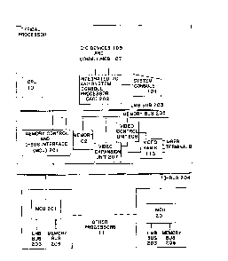
1.5.2 Over~ ot the Fe~ent in~ention:
Referring to Figure 102, an overview block diagram of computers of the
pre~ent invention employed in a distributed computing network, it i9 seen that
CP~ 101 is no longer configured at the hub of all the other elements. Over LocalMemory Bus (LMB) 203, CPU 101 can communicate with integrated I/O controller
(IOC) 202, and memory control and I-Bus lnterface (MCU) 20f, both of whlch
contain sufficlent intelligence to oversee their respective functions without
close supervislon by CP~ 101. MC~ 201 can establlsh connection between LMB Bus
203, IBus 204, and MBus 205, passing data from any one to any of the other two.
.,
: i :
1306~310
Application of Epstein et al
~ .
Communication between computers of the present invention configured as a
dlstributed system, is effected by memory references. All memory locations
within the distributed system are accessible to any CPU-- a CPU may read from awrite to a memory location associated with another CPU on the distributed systemwlth the same facility with which it may access any of the memory locations
as~oclated with itself. All memory access requests from a CPU 201 are passed
over LMB bus 203 to MCU 201, which determine3 from the memory address whether the
desired location is associated with the local computer (the computer containing
the CPU and MCU) or one of the other computers comprising the nstwork. If the
former, MC~ 201 accesses the local memory 102 tor video RAM 113, a~ appropriate)over memory bus 205 performing the requested read or write and obtaining data
from CPU 101 over LMB bus 203 (if a write) or passing data to CPU 101 over LMB
bus 203 (if a read). If the latter, MCU 201 passes the request over I-~u3 204
whence the MCU 201'8 of all other computers on the system examine the memory
address; the computer having that address within its local memory performs the
~-` memory access, the data being passed over I-Bus 204 between the ~CU 201 of the
oomputer having the memory address and the MCU 201 of the requesting computer.
This feature (re~erring briefly to Figure 101) eliminatcs the prior-art need to
have an interoomputer bus (112) connected to and overset~n by the CPU.
An arbltration scheme is provided to ensure that no computer can
monopolize the I-Bus and that no computer can be deprived of the use of the
I^Bu~. This scheme is based on a rotating priority, wherein the computer that
has Just used the bus ls eivsn lowest priority and must wait till other
requesting computers have used the bus before it can-use the bus again.
Inte8rated I/O controller (IOC) 202 contains a microprocessor and is
provided to relieve CPU 101 o~ detail-level 07ersight of data transfers between
the computer and I/O devices 109, and communication lines 107. System Console
; 104 i8 grouped with other user terminals, and is does not occupy the special role
it had in prior-art machines.
LMB bus 203 is provided so that communication between CPU 101, IOC 202,
~ and MCU 201 can take place without contention from any of the memory devices 102
2`~ or 113. Rererences to memory 102 or VRAMs 113 are "passed through" MCU 201 from
~i
~, .
~i -20-
,- 1
~ ` {
~: ~306310
Applicatlon Or Epstein et al
.
LMB Bus 203-to M-Bus 205. Rererences to memory locations of another computer ofthe distributed computer network are "passed through" MC~ 201 to I-~us 204.
Video Control Unit (VCU) 206 is provided ahead of the video RAMs 113 to
relieve CPU 101 of much Or the detailed work Or modifying bitmaps for controlling
displays on user terminals.
Video Expans$on Unit (VEU) 207 may optionally be provided to expand the
pixel size from 8 to 24 bits. VEU 207 includes additional V~AM chlps, but does
not result in the creatlon Or more VRAM locations-- it merely expands the slze
of the existing locations.
~' .
An operating system (not shown on Figure 102, to be discussed in detail
in Section 6) ls provided to facilitate user access to the features provided.
In ~ummaryt the computer Or the present invention is well suited to
distributed processing applications, from two standpoints: one, MCU 201'9
ability to resolve memory requests and honor them regardless Or whether the
desired memory location exists in the requesting computer or some other computer1 Or a network racilitates interconnection and load sharing by a group Or several
Il computers; and two, organization within each computer orrloads functioLs
traditionally perrormed by the CPU and distributes them to other areas Or the
1 computer (IOC 202 to control I/O devices, MCU 201 to handle the details Or memory
-` acoesses and intercomputer communication, VCU 206 to manipulate video bitmaps).
1.5.3 O-errie~ Or the Prererred Eobodiment
In the present embodiment, each computer is a 32-bit computer and is
embodied on a singie 15nx15" printed circuit board. Each board contains its ownLNB Bus 203 which does not leave the board. Each board has a connection to I-Bus
204. Each board h~ a Memory Bus 205 which may leave the board and connect to
, optional expansion memory and video memory boards; up to 2 MBytes Or memory may
' t be accommodated on the computer board and are connected to Memory Bus 205;
-21-
~306310
` Application o~ Epstein et al
~;, ' ,
addltional memory and video memory boards may be connected to the computer
board's Memory Bus 205 to expand each computer's memory capacity.
;
Up to sixteen such computers teach wlth associated memory and video
memory boards) may be accommodated in a single cabinet, the cabinet including a
nbackplane" comprising sockets into which all the boards are plugged, and
permanent wiring interconnecting the sockets. I-Bus 204 is made up Or backplanewiring and interconnects all the computer3 plugged into the cabinet to form a
distributed computer network.
The sixteen computers may share a tot~l memory space Or 512 M~ytes. A~
described above, any Or the computers may access any location Or the 512 MBytes,which may thus be regarded as a "global address spacen.
~.
Figures 103, 104, and 105 together comprise a block diagram Or one
computer board, with CPU 101 depicted on Figure 103, IOC 202 depicted on Figure
104, and MCU 201 depicted on Figure 105.
Rererring to Figure 103, the CPU portion (CPU 101) 's a 32 bit computer
which execute3 microinstructions at a 160ns ma~or cycle speed. It is controlledby a 64 bit microinstruction and uses pipelining techniques for enhanced
perrormance. All data paths, registers and standard accumulators are 32 bits
l wide~ while the FPU registers and runctional units are a full 64 bits wide.
~1
`~1 CPU 101 uses two lnternal non-archltectural buses, A BUS 358 and B BUS 359.
`I These buses conneot the rour maJor subsections Or the computer: MIP
~ ~Microsequencer) 366; ATU (Address Tran~lation Unit) 353; ALU (Arlthmetlc and
;~ Logic Unit) 352; and FPU (Floating Polnt Unit) 351. The B BUS is mainly used for
transrerrlng logical addresses rrom the ALU to the ATU after address calculations
~I have been made. The B Bus also provldes a path to the hardware Referenced and
~l Modified Bit logic 356. The A BUS is primarily used to move data rrom me~ory 102
i;~ (obtained over L~B bus 203, to be disoussed below) through the MIP 366 to the ALU -
352. The A BUS is additionally used ror loading and storing the Floating Point
Accumulators (FPACs) reslding ln FPU 351.
i~'
~,
~`-r, - 22-
3063~
Application of Epstein et al
:
The CPU communicates wi$h other sections Or the board via the LM8 Bus
203, RD bus 362, and EA Bu~ 361. All memory requests are directed through LM8
203 to MCU 201 where the request is either granted locally (if the memory
locations are in the local space), or are redirected to the glob~1 memory bus (an
I-Bus request). A "Read Bus" and "Write Bus" mode is provided on the LM8 which
allcws the CPU and the IOC to communicate without any memory response or
interference. The I-Bus type request provideQ the path to attached computers and
intelligent I/O servers.
The XD and EA bu~es allow IOC 202 to initialize CPU 101 by dlagnosing,
loading and verifying CPU Microcode Control Store 369. These are
non-architectural buses; that is, they support internal, underlying functions and
do not directly bear upon the execution of any user-invoked runctions. The XD is
a bi-directional data path which multiplexes its 16 bits onto and Orr or the 64
bit u~ord bus. The EA path is the address path for the Control Store 369 RAMs.
'I
CP~ 8lock Diagram Summary
ALU- ALU 352 is a full 32 bit ALU inoluding 13 GP registers, a
shlrt reglster and a self incrementing PC. Most
operations are co~pleted in a 160ns cycle with the
remainder Or operations requiring 240ns. It is
j implemented in a 135 pln PGA package.
`" MIP Microlnstruction Processor (MIP) 366 is a 15-blt
~ pipellned microsequencer along with an instruction
`~l prefetch unit (enqueues, cracks and dispatches on
macro instruction~), the MY Architectural Clock, the Real
~- Time Clock (RTC), and a memory data unit whlch accepts
i~ data from the local memory bus. The MIP contains
: ~ selrtest logic and provides a test-OK pin which is
checked on power-up. It is implemented ln a 179 pln PGA
package.
AT~- Address Translation Unit (AT3) 353 contains address
translation and memory address logic (including address
protection support) in addition to a 16 entry ATU cache.
¦ FPU- Floating Point Unlt (FPU) 351 is a 64 blt floating point
! computer chlp lncluding the 4 Floating Point Accumulators
(FPACs~, a full double precision data adder with
rounding, truncation, prescaling, exponent and
normalization support. Thls chip rits lnto a small 64
pln PGA package. `
~.,. :
~3
3 -23-
~ i
~ ~,
,
uStore (Micro~tore) 369 -
a 16~ x 64 bit RAM eontrol store, including a parlty bit
whleh is loaded 16 blts at a time. It eomprises 70ns
8Kx8 SRAMs.
loek Generation -
a multiphased elock based on 80ns basie system cloek
whieh generates a 160ns microcycle. A mieroprogra~mable
stretch to 240ns i8 used for longer oPerations.
eratehpad 365
a 2Kx32 RAM area used rOr mieroeode temporary.ar,d
oonstant ~torage area. It eompri~es 45n~ 2Kx8 SRAMs.
oeal Mem Bu~ Control (latches 354, 355, 364)
Interraoe logic to ~atch the ATU and MIP memory eontrol
si~nal3 to the LMB protocol. This interrace also lncludes
hardware eontrolled refereneed and modified bits whieh
~upport up to 16 MBytes of loeal memory without ~ieroeode
support.
uStore De-mux 370
Memory Portion
Logle for loading the eontrol store via the XD Bu3.
The Memory portion Or the board eontains the main memory control unit
(MCU 201) and 2 Megabytes of main memory 102 itselr. The MCU also provides the
eontrol Or the MBus and the eontrol for the global I-Bus (to be deseribed
below). The MBu~ is A1so the conneetion for blt mapped video sereens that are
attaohed to the main memory addre~s spaee (~ee seotlon 5). The only
eommunication path between CPU 101 or IOC 202 and MCU 201 is the LNB, deseribed
ln detail in seotlon 3.
The Memory portion ls entirely eontrolled by two 8ate arrays: CMOS-MEM
gate array 561 and Bipolar-MEM gate array 562. Since the rormats and protocols
on the varlou~ buses are eontrived to facilitate pas3lnt rrom one to the other,
these two gate arrayq are basieally trar~ie directors and error cheeking devieeswhlch control l l the lnteractionq that take place among the LMB, and I-Bus and
the MBus.
13063~0
Application Or Epstein et al
The LMB and the I-Bus are the two busses that can initiate memory
operations. The LMB initiates all local memory accesses while the I-Bus
initlates all accesses Or this particular node from other global nodes. The MBus
is essentially an lnternal bus to this memory portion which carries the actual
address and data Or the local RAM's themselves. This bus is "rawn, unallgned,
uncorrected data which is stored in the RAMs themselves. This MBus has expansion
capablllty 80 that up to 16 Mbytes can be addressed by this MCU (the two gate
arrays) without adding more control. Thus, the MBus goes ofr-board 90 that
additional memory can be added either in the form Or standard DRAHs or in the
form of memory mapped sraphics.
.
To illustrate the flow Or a memory aQcess~ consider a CPU reference. The
rererence is initiated by ~he CPU via the LMB. The MCU (combination Or CMOS andBipolar MEM gate arrays~ recognizes the start Or the memory operation. It then
makes a determination Or whether the rererence was a local reference - i.e. to
this node - or a global reference. Assuming it was local, the M W generates the-~` proper RAS and CAS (row address and column address) llnes to acce~s the required
data. (The RAS and CAS llnes are part Or the MBus, and will be discussed in
detail in Section 4.j Elther the memory array cn the board ltself (2 Hbytes) oran external expansion memory on the MBus will respond with the data. The MCU now
dlrects that data back onto the LMB and signals the oomputer that the data ls
available. Ir the data required allgning or correcting, the MCU would have taken
the data lnto the gate arrays themselves, manipulated it as required, and
rebroadoast the data baok onto the LMB prior to signaling the computer.
~ ad the rererenoe been global - i.e. not for this node, then the MCU
would not have issued the rererence on the MBus. Rather, the MCU would have
begun arbitrating and re-initlatlng the reference onto the I-B w . The responding
' I-Bua node will return aligned, corrected data back vla the I-Bus at which tlme
- the MC~ will direct the data back onto the LMB, bufrering the data as necessary.
., :~
Memory Blook Diagram Summary
The memory portion Or a computer board is deslgned around MCU 201 which comprises
two 8ate arrays:
-,
~ ~ .
~ -25-
.,
~ . - - :
:
~ ~ ~ 1306310
,~. .
Application Or Epstein et al
CMOS-MEM 561
This Fu~itsu CMOS C8000VH series gate array is
implemented in a 179 pin PGA package. Its main runctiOns
include: Error Detection and correction circuitry
tcorrect all single bit errors and any touble bit errors
that contain at least one hard bit failure); Refresh and
- snipr control; Read-Mod~fy-~rite control; data
alignment; interrupt and special function control.~
~ . .
~ipolar-MEM 562
This Motorola 2800ALS series gate array is an ECL
internal gate array. This primary MCU control chip is
necessary for high speed response to memory requests.
The ma~or functions of this array is: Address
recognition; Data flow direction; Bus arbitration (both
i Bus and LMB); initial Address generation; and Error
detection (correctlon is done in the CMOS array).
MBus 205
The Memor~ Data Bu~ is the common data path for
transmitting data to and from all syste~ memories 102
(including the 2 Megabyte~ that can be on-board) and
VRAM~ 113.
`1, LMB 203
~`1 The Local Memory Bus is the communication path from the
looal comput;er (CPU portion) and from the local I/O
portion. T~is is a specified bus interface which is
- I recognized ~r the MCU and is described in detail in
section 3.
~-' IBus 204
~i This I-Bus is a global memory bus which connects computer
~ nodes vla a common memory space. Section 2 describes
,~ ' this bus in detail.
Main Memory 102
The Main Hemory block repre~ents 2 Mbytes of 256R DRAMs
~; organized into 512~ x 39 blts. The 32 bit data words and
7 ERCC blts implement a portion of the memory address
space. It i9 two way interleaved to enhance consecutive
~ccess performa~ce. Additional off-board memory may be
connected to MBU8 205; this may addition 1 main memory
i 102, or YRAMs 113 for storing screen bit maps (see
section 5).
~- Integrated I~O Portion
i IOC 202 (Figure 104) i8 designed to 3upport the base system I/O devices
as well as SCP tsYstcm console proce~sor~ functions. This subsystem, run by a
. . .
.~,
~` 4
;~, -26-
~1 .
` 1306~0
~:
Appllcation Or Ep~tein et al
:.
microprooessor, i8 the only lntelllgent part Or the board upon power-up. Its SCP
functions include: booting the rest Or the system (including CP~ microcode
load); acting as a system console computer during normal run time; and
; diagnosing the system on railures. The I/O function provides the board with
device support for the basic integrated I/O derices. This includes:
- an SCSI (small computer standard interface) Bus Host-Adapter
Interface 468
- an SA400 Floppy Diskette Controller 467
- an Ethernet IEEE802.3 LAN Controller 480
- Four RS232C Asynch Channels 459 (1 w/modem support)
, :
- a parallel Printer Port 460
- a battery-backed-up Time-or-Boot Clock/Calendar 457
:,~ ,.. .
~t3i The Local Me~ory 8us Inter~ace is the primary communications ch~nnel
between CPU 101, IOC 202, and MCU 201.
~j
The integrated I/O subsystem is centered around the 80186 microprocessor
451 and its associated 16 bit uPAD (microprocessor Address/Data) Bus 465. The
microprocessor co~trols the power up sequence by holding the CPU portion and
i Memory portion or the board in Reset state. (This microprocessor is the sole
`~ controller Or the system RESET signal whlch resets all IBus nodes as well as this
oomputer node.) Uslng mlcroprocessor rirmware stored ln the power up PROMs 452,
lt does a selr-check, verlrylng enough Or this section to read more
~ mloroproce sor rlnmware Orr o~ a disk into the ucomputer RAN Nemory. Any railure ~ ~-
c to thls point will be displayed on the front panel LED 458 which is under control
~ Or the 80186.
:.y -.:
`;~ Once the uP Memory i8 loaded with a full complement Or firmware, a more
~i complete power-up diagnostic is run, including the MIP gate array selrte~t pin
(see CPU seotlon), other CPU testing, memory testing and vldeo dl~play
lndlcatlons. The microprocessor then boots ln host mlcrocode rrom the boot
devlce (Floppy or SCSI Winchester) into the CPU control store using the XD and
EA Busses. It then rinishes the power up diagnostic testing and starts the CPU.
:
-27-
~306310
Appllcatlon o~ Epsteln et al
'
Durlng normal run tlme, IOC 202 serviceq devlces connected to it. All
communication with CPU 101 takes place through buffer 484. CP~ 101 rorwards
requests over LMB 203 u~ing the ~RITE BUS function to be explained below, which
does not involve MCU 201 or memory 102 but which results in writing into buffer
484. The microprocessor does the interpreting, scheduling and device control Or
these request3 in parallel to normal cPn execution. To aid in thi function, the
IOC includes a DMA channel 476 directly connected to the LHB for
non-host-assisted main memory accesses. In this way, the Integrated I/O
subsystem is acting as an independent I/O computer to the host. Data for outputare likewise placed by CPU 101 into buffer 484. Input data are placed in buffer
484, from which CiU 101 may read them over LHB 203 using the READ BUS function
(explained further below) which does not involve MCU 201 or memory 102. The
WRITE BUS and READ 8US runctions of LMB 203 eliminate the prior-art need
~re~erring briefly to Figure 101) to have an I/O bus and a memory bu3 both
connected to and overseen by the CPU.
Integrated I/O Block Diagram Summary
80186 microprocessor 451
All the integrated I/O device~ are managed using the
Intel 80186 microprocessor. The main purpose Or he
' microproce3sor is to rield I/O requests, supervise I/Odata trarric ~ provide I/O status on completion of a data
~i~ transrer. The microprocessor also Eives the systempower-up ~ diagnostic intelligen¢e with which to
load/verify Control Store RAMs.
The 80186 microprocessor ~eatures include: a 16 bit data
bus; 2 integrated DMA controllers and interrupt support.
It ha~ a 1 Mbyte address space which allows all the I/O
' `~ controller~ to be memory mapped as well as the CPU; Control Store. The 80186 will be run at 8 MHz in order
``3I to maximize its perrormance.
Power-up PROM 451 and N W RAM 453
The Integrated I/O portion contains two 2KX8 PROMs and a
non-volatile RAM (32x8). The PRONs are used for power-up
diagnostics and a Floppy/SCSI loader to complete the
power-up procedure. The N W RAMs (non-volatile RAMs) are
used to store configuration informatlon, serial numbers
and LAN adtress information to reduce hardware ~umpers
i ant repetltious user lnput.
uP Memory and Buffer 484
~ ~ .
. ~,
` ' - 28 -
.
-: 1306~,10
Appllcatlon Or Epstein et al
.:, .
Thls 18 a 32 KByte shared memory area. Approximately
two third~ of thls space i9 used for 801 code to control
-j the LAN, I/O devlces, Host Interface, and SCP
functlonality. The remainder of the space i9 used for
data buffering to lnsure high bandwidth burst data
movement support.
The RAM consists of four 8Kx8 CMOS statlc RAMs with
access times of 70ns. The bufrer 18 conrigured to be a
16Rx16 bit ~pace frcm the 80186JLAN side and 8Kx32 bit
space from the Loc~l Memory interface side.
~; The buffer memory system will bs shared by LAN, Local
Memory and 80186 DMA vla tlme slot allocation. Data is
packed into the buffer ln DG format. (lower addressed
bytes are leftmost). A byteswap/wordswap is performed at
a 3et Or transceivers between these RAMs & the UPAD bus.
~ This allows the LAN & the 80186 to access the contents of
3 the buffer witbout having to perform software
byteswapping.
~ LMB DMA Control 476
-~ Communication to the Local Memory Bus (LMB) is controlled
by this part of IOC 202. The LMB provides a path both to
main memor~ and to CPU 101. :
For oommunication to main memory, this section provides a
direct memory aocess state maohine which does not require
80186 firmware control. A 9-bit DNA Double Word Counter
1 and an address pointer/counter is provided to facilltate
the transfer. Eaoh memory access i~ either a double word
(32 bits) read or double word Nrlte. By loading the DMA
Double Word Counter with a number between O and 511, up -
to 1 page t2Kb) of data can be transferred at one time. ~ ~
This interface will support a transfer rate of 7.6 ~ -
~2'; Mbytes/second.
Integrated I/O to CPU communication is handled by Special
Read and Special Wrlte commands on the LMB (RX and WX).
(See Section 3.) (Nemory residing on the LNB will not
ï respond to R~/WX commands which allow non-memory
operations.) The I/O to CPU communication is
acoomplished by the CP~ reading and writing to the uP
Memory and Buffer (see above) via RX and WX commands on
the LMB. Blooks of data are loaded into or read from
that buffer by the CPU which then signals the 80186 via
~ an interrupt line. The 80186 then processes that data
;~ block in an appropriate manner (specified by the data
bloo~ itself), and, in turn, the 80186 will signal tbe
acoeptance or completion of that block via a dedicated
signal to the CPU which causes a micro level trap
(microcode visible but not macrocode visible).
~ L
'~
, ~ .
-29-
.
:~ ~306310
Applicatlon Or Epstein et al
Flop W Disk Controller 467
Support is provided ror two 5.25" Floppy Diskette
drives. The target drives record data at 96 TPI and have
a 737.28 KByte capacity. -
The dri~es will be controlled by the Fu~itsu MB8877
Floppy Disk Controller chip, pac~aged in a 40-pin DIP.
The microproce3sor initiates all floppy disk operation3
while the MB8877 chip itselr perrorms DMA transrers
between Floppy disk ~ the Buffer RAM area utilizing one
the microprocessor's DMA ports. The Floppy controller
has priority over the SCSI DMA Channel since the SCSI
tranfers can be held orf indefinitely.
,,
The SMC FDC9229BT Floppy Interrace Chip, which performs
the runctions o~ write-precompensation, digital data
separatlon ~ head-load delay i9 u~ed in con~unction with
the MB8877 chip.
`/ :
SCSI Bus Controller 468
The SCSI Bu~ Controller provides access to SCSI
compatible devices, particularly Winchester type disk
~i drlves and magnetic tape drives. The SCSI ~u~ Inter~ae,
~i5i acting in a Host-Adapter mode, allows up to 7 SCSI
Formatter cards (Controllers, CPU's, etc.O to be
~ connected together on the SCSI Bu~. This bu~ is 8 bit3
d wlde (plus parity) and trans~er~ data at a an
~! Asynchronous rate ~r 1.5 MBytes/sec. Drivers and
i! receivers are slngle-ended.
¦ ` The controller chip i-~ the NCR SCSI Protocol controller.
¦ This controller per~orms DMA transrers between SCSI and
the RAM Bufrer area by using one Or the 80186 DMA
¦ channels.
LAN Controller 480
The IEEE 802.3 CSMA/CD Loc~l Area Networking protocol is
¦ - supported. This communications protocol ls rated at 10
; - MBit per second utilizing coaxial cable. ~p to 100
¦ statlons may be connected together using a miximum cable
length of 500 meters. It i8 lmplemented using the Intel
82586 LAN Controller ~ the SEEQ 8023 Manchester
Encoder~Decoder.
.
The Intel 82586 LAN controller chip fully implements the
IEEE 802.3/Ethernet Data Llnk speci~ication. On-chlp
~ control includes DMA ~emory management and microprocessor
j hold-ofr control allowlng it to operate as a cocomputer
on the UPAD bus and using the same RAM Buffer as the
i 80186. The SEEQ 8023 Manche~ter Encoder/Decoder
completes the Ethernet interrace by connecting directly
¦ to the Intel 82586 on one slde and to the Ethernet
transcelver box on the other 3ide.
~ j .
' -30-
'`~` '
:, .
;~
i306310
~ .
Applioation Or Epstein et al
, ,~ . .
. ..
Ethernet node~ are identified by a distlnct 48-blt
address. The high 24 bits are fixed for Data General
Corporatlon at 08001B (~EX). The low 24 b1ts are set
indiYidually with the board's serial number during the
manuracturing prucess. This number is stored ln NOVRA~s
453-
The integrated I/O portlon supports 4 R æ 32C Asynchronousport~ 459 uslng two Signetics 2681 DUARTs. Each DUART
provides programmable reatures which include:
Independent baud rates; Data format seleotion
(bits/char, stop bits and parity selection); duplex
selectlon; and overrun detection.
Of the four ports, one is full-reatured, including modem
control, a second 3upports hardware Busy, and the
remaining two are simple, requiring ~ortware Busy
control.
:
IOC 202 supports an 8-bit parallel printer port. Either
Centronics type or Data Products type parallel devlces
can be connected to this port.
Th Ricoh RP5C15 Clock/Calendar chip is used to provide ~-
the system with the current time ~ date during the boot ~ -
procedure. The l2V at 15uA required to keep this chip
backed up while standard power is not applied must be
8upplled to the board via a backpanel pin. This will be
provided by 2 AA cells found iD a user-accessible
location. The Time of Day and Date will be accessed once
during power up. The time is then kept track Or by ths
ho8t ltselr Thi~ chip can be read only via the SCP once
the 8ystem is up, but can be written under bost software
or SCP control.
The 80186 directly controls the display Or a 7 segment
LED located on the front panel 461. The decim2l point
of the LED is a POWER-OK indicator and will be lit when
the 80186 detects POWER-O~ as signalled by the power
supply. Tbe 80186 firmware directly controls each Or the
7 segments Or the display which will be used to signal
railures detected during the microprocessor~s diagnostic
procedures.
. ~
Operating Systems
:
,
~ -31-
1306310
Appllcatlon Or Epstein et al
. ~
Operating Syste~ (OS) 501 and the AOS/VS operating sy~tem (a prior-art
operating system marketed by Data General Corporation) will both run on the
system. OS 501, however, i8 the target system and thu~ will be designed to takeadvantage of certain reatures not currently supported in AOS/VS. The major
sOrtware reatures include: ~ ~
- All 8it Mapped Graphic displays
- ~NICORN lnterraces ror integrated Printers, Disks and
Tape~
- Auto-Power-~p with automatic system generation, sizing,
configurations and date/time
I - I-Bu~ support Or attached computers and foreign
operating system enviroDments
- Extensive Windowing support
~;1 - LAN based transparent file and computer sharing
~33
- Hhltiple OP~S computer support
AOS/VS will require some modirication in I/O device handlers. There
will, however be a device code 10 and 11 emulator built into the hardware for
compatlbillty. this emulator is neither efricient nor expected to be permanent,but rather, included to help in the transition away rrom the 10 and 11
!~` dependenoy.
.,
;~ All standard sortware languages and higher level program applications
will run unmodirled.
.
f
' ' ,'
~ 1 .
:: .
:
~-3
``.`.i
~ 33~
`, -32-
':"
130fi310
~ Appllcation Or Epsteln et al
; 2. Det~led De~cription Or NCU 201
. .
The I-~US, or Interface Bus, is a 32-bit interconnection
system for processors and memory. The I-BUS allows nodes (such as
proces~ors and memory controllers) on different P.C. cards to
talk to each other.
Physically, the I-BUS is a set Or wires connecting two or
more P.C. boards in a single chassis. The nodes talk to each
other (that is, send or receive data) over these wires. Each node
has its own MCU 201, which forms the lnterface to the I-BUS.
This interface takes the data and data requests from the node
and translates them into the proper protocol to send on the
I-BUS. The protocol determines what can be sent, when and where it
can be sent, who can send it, and how it can be sent.
'`'`1 :
This protocol is what make~ the I-BUS conceptually
unique from any other data bus or set of Ju~per cables. It
', i9 intended to achieve the following:
+ One common backpanel syste~ for all processors
+ Transfer capabillty for 8 bits, 16 bits, 32 bits, and 256
(8x32) bits
+ Plpelining of priority arbitration
+ ~quality in bus access for all nodes
+ Able to support up to 16 nodes
+ High transfer rate
+ Multiproces~or and attached processor support
Fault detection
+ Simple to reconfigure
+ Designed to work as extended memory bus in MV arohitectural
environment
2.1 Sectional Overview
~'
-33-
~306310
Application Or Epstein et al
Definitions
''",
To aid in understanding the following information, a li~t of
oommon terms and their definitions is given below.
;, Node
An entity conneoted to the bus that drives and/or
~> monitors signals on the bus llnes.
Baokpanel
~¦ A p.c. board that runs parallel to the back of the card
-~'l cage. It contain~ the interconnections between the
~;~i indlvldual cards as well as the sockets into which the edge
;~ oonnectors on the cards are inserted.
Slot
~ A location on the backpanel into which a p.c. card is
; lnserted. A node can occupy more than one slot, but each slot
`1 ¢an belong to only one node.
Arbitration
sing a priority system to determine which node will be
allowed to use the bus next when two or more nodes request
~l the bus at the same time.
-'i Master
~; The node that has gained control of the bus.
~ ~l
j Slave
The node responding to a command from a Master.
Requester
A node that 18 requestlng use o~ the bus.
,. i
` ~ Transactlon
One complete operation on the I-~US, usually involving
trans~lsslon Or data ~rom one node to another.
Phase
Several phases c~mprlse a transactlon. Each phase
represents a specl~lc event durlng the transactlon, such as
~l an Arbltratlon Phase.
:`1
Perlod
One full cyole of the bus clock slgnal.
~l Inter~ace
The physical part of a node that 18 directly attached
to the bus and i~ responsible ~or sending and receiving
bus slgnals. The inter~ace usually acts as an intermedlary
-
. . .
" -34-
". ..
,,
r ~ _
13063~0
Appllcatlon Or Epsteln et al
`c - between the bus and a local processor or memory,
~-~ translating local commands lnto the necessary bus protocol.
;..
~,~;, .
~ 2.1.1 Purpose
.
,
., - ' '
The primary purpose of the I-~US is to allow fast
communication between indivldual processor nodes and distributed
global memory in a 32-bit system. AD explanation of those
partic~-lar goals stated in the introduction is li~ted belcw~
.~ - , .
:`'j ' ~ " ~, ~:
One common backpanel system for 1l processors:
; The one set Or interconnections on the backpanel will
; bandle all processors.
; I Transfer capability for ô bits, 16 bits, 32 bits, and 256
3 (ôx32) bits:
Bus instructionq will be available to transmit data in
~ the previously listed sizes.
;~ + Pipelining of priority arbitration:
Determination of which node will get the bus next can be
done before completion o~ the current bus operation.
+ Equality in bu~ acee~s for all nodes:
No node can monopolize the bus;
No node can be deprived of the bus:
~sing a dynamic prlority system (instead of fixed
priority,
Every node is guaranteed periodic acoess to the bus.
j .
Able to support up to 16 nodes:
This is the ab~olute maximum for a single cha~sis
system. Typical ~ystems will have fewer than 16 nodes.
+ High transfer rate:
~` The bus clock frequency is ôO ns. The maximNm transfer
rate for single transfers is 25Mbytes~s and for block
transfers is 44.4Mbytes/s.
+ Multiprocessor support:
The bu~q protocol supports multiple co-equal independent
prooessing nodes.
r
+ Fault detection:
Byte parity will be provided with all data transmission.
, .
:
,'i,
-35-
```1
306;~10
~ Applicatlon Or Epstein et al
~, . . .
Simple to reconfigure: -
No ~umpers are required ln slots tbat are not filled.
Also special lnstructlons wlll make lt easy to determlne
upon lnitlallzatlon the properties and capabillties Or
each node on the bus.
De~igned to work as an extended memory bus ln prlor-art MV
architectural environment:
~' The I-BUS addresslng scheme is compatlble wlth the
i~ physlcal addressing mode ln MV archltecture.
''I .' ~
.j
-~i An efrlclent use of the I-BVS i9 ln a system where each
node executes out Or its own local memory. Ir one or more
processors requires an I-BUS acces~ for each operation, system
~;~l perrormance can be severely degraded. As will be discussed ln
8eotion 6, the operating system racllltates allo¢atlng data to the
local memory Or the node where the programs accesslng that data
most frequently are executing.
!~,
i;,
, 2.1.2 Signals
.
~, .
2.1.2.1 Signal Groups
' :
Physloall1, the I-BUS conslsts or 61 lines. These are
dlvlded Into three groups: data/address llnes, bus arbitration
~; llnes, and utillty lines. Below i9 a breakdown Or the three
groups. (The ^ symbol appearlng before a slgnal name means that
the signal is "low-truen.)
.~ I
.j ~
`~i -36- ~:
.
,, :
1306310
- Application Or Epstein et al
.
, .~,
~ Data/Address:
, .
32 ^DA<0-31> data~address llnes
4 ^PDAC0-3> byte parlty Or data/address lines
1 ^AV/^MM address valld~Master wait
1 ^SWAIT Slave wait
1 ^XV transaction valid
; Bus Arbltration:
16 ^BREQ<0-15> bus request lines ~ -
1 ^B8SY bus busy
~tlllty:
1 ^ARBRST arbltration reset
1 ^BUSCLK bus clock
1 ^CACHE encache
1 ^PWRFAIL power fail
1 ^PWRUPRST power up reset
total 61
~:,
2.1.2.2 Data~Address signals
There are 39 slgnal lines in the data/address group. They are as
' rOllOW8:
DA<0-31~ - Data/Address
These are used for the aotual transmission Or the address and
data.
PDA<0-3> - Parity
These contain the byte parity 8enerated during data and address
transmisslon.
`'
; AV/MW - Address Valid/Master Wait
Thls is used by the Master to tell the Slave that an address is
~- present on the Data/Address lines.. !
: :.
SWAIT - Slave Wait
This 19 used by the Slave to tell the ~aster that it is not ready
for the next transmlssion Or data yet.
~.~
r
~
: ~
~ -37-
:1306310
; Appllcation of Epsteln et al
~ XV - Transaction Valid
,`' ;?J~ The Slave uses this to let the Master know that no error has
, been encountered ln the processing Or the current reque3t.
i`~ Errors can include: bus parity error, illegal request, or
multiple bit errors in memory.
~j 2.1.2.3 Bus Arbitration Signals
`f, There are 17 lines in the Bus Arbitration group. They are as follows:
,t: ~ .
BREQ<0-15> - Bus Request
- These are used to request the bu3 and to determine who will be
granted access to the bus next.
i,
- BBSY - Bus Busy
~; This i9 used to indicate that a node is currently using the bu~.
It is driven by a Master.
. .1 .
.,~ . .
~, 2.1.2.4 Utility Signals
~.
! There are ~ive utility signals on the I-BUS. They are a~ follows:
.~1
`^l ARBRST - Arbitration reset
~;~ This causes all nodes to reset their priority to the lnitlal
value after startup.
BUSCLK - Bus clock
~, This signal is generated by only one node and ls sent to all
~`¦ nodes. It is used to synchronize and clock all actlons on the
I-BUS.
~ CACHE - Encaohe
.,~
. .
.,.
-38- ~
.. 1 .
` ~
:~;
` i~06~0
Application Or Epstein et al
.... .
This is used to tag data as belng encachable for processors with
local caches. ~
PWRFAIL - Power railed -
This slgnal is asserted by the power supply when it i8 determined
that a power 1099 has occurred that ls sufricisnt to arfect the
bus.
PWRUPRST - Power up reset
This is provided by the power supply to lnform the nodes that the
system has ~ust powered up.
2.1.2.5 Signal States
All slgnals on the I-~US use "low-true" implementatlon. That is, a
slgnal is consldered activated, asserted, or representing a "logic 1" when
there is a voltage pre~ent corresponding to a low TTL voltage level. A signal
19 considered released, de-asserted, or representing a "loglc 0" when there is
a voltage present corresponding to a hi8h TTL voltage level. ~hen rererring to
the actual electrical content Or the signal line, the ^ ~ymbol will appear
berore the signal name indicating its low-true status. When describing the
logical contents Or the signal line (1'8 and 0'9) the ^ will not appear with
the slgnal name.
2.1.3 Address/Data
2.1.3.1 Normal Address Space
As will be described in section 2.5, "Commandsn, command encodings are
provided to access "normal spacen, and "specl~l spacen. All system memory is
part Or normal space.
-39-
~- 1306310
,,~ .
r Application of Epstein et al
;~ The I-BUS operates in an addressing mode corresponding to that Or the
physical addressing mode Or 32-bit prior-art ~ECLIPSEn*systems manuracturedby Data General Corporation. Physical addresses generated by ECLIPSE
address translators correspond to the addresses that appear on the I-BUS.
The I-BUS has a limit Or 512M bytes Or normal addressing range. This
is typically organized in double word format; that is, each memory location can
be thought of as being 32 bits wide (two t6-bit words). Individual bytes and
single words can be accessed as well as double words and blocks Or 8 double
words.
The 512M bytes Or addre3slng range is divided lnto 4096 segments Or
128K bytes each. Each node on the I-~US will be assi8ned one or more Or these
se8ments ror its own address ran8e. Ir a node has less than 128K bytes Or
physical memory available, lt wlll be assigned more than it actually needs. In
that case, it will be up to the requestlng node to kncw the correct range.
Asslgnment 19 done by a slngle de~lgnated Master node called a System
Conflgurator Node. Asslgnment 19 done a~ter a node has po~-ered up and performedall necessary looal lnitlallzatlons. m e lnitial memory assi8nment usually
remains with a node unless there i8 a power railure or a system reset.
It is not necessary that all 4096 segments get asslgned somewhere.
~owever, Master nodes must take responsiblllty ror generatlng valld destinatlon
addresses.
.
All addresses are aocompanled by parity blts. m e data~address lines
are dlvlded into 4 groups o~ 8 llnes wlth eaoh group havlng lts own
oorrespondlng parlty llne. Parity llnes generate odd parlty for both address
and data trans~lsslon.
2.1.3.2 Speolal Space
Whlle system memory is, as descrlbed lmmedlately above, addressed as
normal spaoe, the primary rea~on ror speolal space is to allow acoess to things
* Registered trade-mark
~ -40-
`:
~306~310
-` Application of Epstein et al
i: .
s' .
.,,~ . ,.
such as proCeSQor registers, PROM, or static RAMs by assigning addresses to
them. Special Space access wlll be handled through special commands. ~ata can
only be read or written to Special Space in 32-bit even double-word format.
Each node's special space is addressed by a combination of the node ID
number and a 23-bit offset. Thus, each node has 8M (32-bit wide) Special Space
addresses available, regardless of how much normal memory space addressing
range has been assigned to it.
The upper 16 locations of each node's special space are reserved for
certain interface registers used during I-BUS operation.
2.1.3.3 Data transmission
Data can be sent across the bus 8 bits, 16 bits, or 32 bits at a time.
For 8 or 16 bits, the contents of the remaining data lines will be undefined.
The four parity lines generate odd byte-parity for data transl~ission in thesame manner as for address transmission. For 8 and 16-bit transmission,
correct parity will be generated for all 4 bytes.
~ ach data transmisslon can take as long as needed. One control line is
used to hold up the bus until the sender can place the entire data on the bus.
Another oontrol line is used by the receiver to hold up the bus until it is
ready to receive the data.
2.1.4 Bus Arbitration
Priority arbitration follows these rules:
1) When two or more node3 wish to use the bus at the same time, the node
with the highest priority is granted access ririst. If only one node is
requesting the bus, it is granted access regardless of its current
priority.
2) The last node to access the bus becomes the lowest priority node. The
node following lt becomes the highest priority node.
-41-
.
~ ~` 1306310
;;~.
Applicatlon of Epsteln et al
* 3) PrioritieQ are assigned from highest to lowest with the same
- progression order as that of the slot numbers ~0,1,2.. 15). Slot O
always follows slot 15 on wraparounds (e.g. 5,6..15,0,1..4).
4) Each access can conslst of one of the following:
A single 8, 16, Or 32-blt transfer
A single block (8x32) transfer
A bus locking operation (such as a combination read-wrlte)
Below ls an example of a sequence Or requests and the res~lting
arbltrations.
2~ode(s) requesting Current prlority Node granted access
idle 6,7.. 15,0,1.. 5 ---
3 6,7.. 15,0,1.. 5 3
3,5,6 4,5.. 15,0,1.. 3 5
3,6 6,7.. 15,0,1.. 5 6
3 7,8.. 15,0,1.. 6 3
idle 4,5.. 15,0,1.. 3 ---
0,1 4,5.. 15,0,1.. 3
1,2.. 15,0
2,3.. 15,0,1
ldle 2,3.. 15,0,1 ---
Immedlately after initialization, the node in slot O will be the lowest
prlority node. It is not necessary to have all slots filled ln order to
arbitrate properly. Any unused slots will be ignored during priority
arbitration.
Priorlties do not change when the bus is idle.
2.1.5 I-PUS Operation
--42--
.
' ', ' ~. ' "'...... ~ `' : '
`~:
~306310
Application Or Epstein et al
2.1.5.1 Node Register Requirements
,..
; Each Or the nodes on the I-BUS are required to have several reglsters
available for access by other nodes on the bus. m ese registers are used to
~tore I-BU$ specific lnformatlon. m e registers are asslgned address
locations in speclal space. They are then acce~sed through normal special space
commands. Since most of these registers are less than 32 blts wlde, they are
returned ln the low order DA lines with the upper lines ignored.
Many of these are control registers and not true memory locations.
Some have restrlction~ on global acceqs and some perform special functions when
written to. m ese special characteristics are summarized in the following
register descriptlons: `
Memory Base Regi ter (Location 7FFFFD)
This contains a 12-blt number that corresponds to the starting
segment Or addressing range for that node. m is is read/write
~ccessible to any Ma~ter.
ID register (Location 7FFFFF)
This oontains a 16-blt code for the type Or board that the node
represents, for example: processor, memory, etc. Thi3 is read
aooessable to ary Master (writ are undefined).
Node Number Register (Locatlon 7FFFFC)
This contains the 4-bit node number assigned to the interrace when
it powered up. All special commands are addressed to a node by its
node number. This is read accessible by any Master (writes are
undefined).
Memory Size reglster (Locatior. 7FFFFE)
A 12-bit register containing the local memory size in 128K-byte
blocks. This is read/write accessable to any Master.
Interrupt register (Location 7FFFF8)
-43-
1306;~10
`: .
~ Application Or Ep~teln et al
:
-~ A 16-bit register for interrupt requests from other nodes. Each
bit can represent an interrupt request from a node with the
corresponding slot ID. This is read/write acce~sable to any Master.
Writing a "1" to any bit will set that bit, whereas writing a "0" will
bave no effect.
Mask-out register (Location 7FFFF7)
A 16-bit register for bits to mask out those Or the Interrupt
register. Thls is read/write accessable to any Master.
Status register (Locatlon 7FFFF9)
A 16-bit register conta~ning status bits for things such as
initl~1izatlon, hardware resets, and errors in transmission or
commands. Thi~ is read/write accessable to any node. Writing a n1" to
a bit will clear that bit, whereas writing a "0" will have no effect.
Data Latch (Not accessible in Special Space)
A 32-bit register containing the last 32-bit double-word written to
that node. This is read accessable to the local node only. It is
written to impllcitly on every memory write to that node.
InterPaoe Status register (Location 7FFFFB)
A 1-bit register indlcatlng whether or not the lnterface is fully
funotlonal. This is read/wrlte accessable to the local node only.
Loopback Control Register (Location 7FFFF6)
Any write to this 1-blt register will inltiate the Loopback
dlagnostic sequence. This is used for testing the data path of the
node. The next command to that node will use the data latch, that is,
any data stored or read will be to or from this register. The node's
data latching and address deooding cirouitry can be tested without
disturbing any internal memory locations. This is read/write
aooessible to any Master, however any command will reset the sequence,
; so there is no point in readlng the status of the loopback control
register.
-44-
, .
:
~: ., - .~ ~-
- ~ 13063~0
` Appllcation o~ Epstein et al
:
Global Access Enabled Register (Location 7FFFFA)
This 1-bit register controls a node's acceQs to remote memory
locations through the I-BUS. If this regi~ter contains O, the node is
prevented from making any memory references on the I-BUS. If this
reglster contains 1, the node ls allowed to make memory references.
This register does not prevent special space accesses. This register is
read/write accessible to any ~aster.
2.1.5.2 Power-up
The power supply determines when the individual nodes may begin bus
initialization. A single node, determined by system configuration, begins
sending the bus clock. Bus clock frequency is set at 80ns. ~hen the bus clock
appears on the line, each node undergoes a self-test. If the self-test i~
complete, the node can place itself o~rline.
At ~his polnt, the system configurator node will begin issuing commands
to the other nodes in the system. The system coDfigurator node will run a
dlagnostic test to make sure that all nodes are operational. It then
determines the memory requirements of each node and assigns the appropriate
address ranga. It will also issue an arbitration reset that initializes the
priorities o~ all the nodes (giving itselr the lowest priority).
The system coDrigurator node does not necessarily have to generate the
bus clook signal.
2.1.5.3 Normal Operation
Bus operation is divided into rour phases. They are as follows:
Arbitration phase
Each node inspects the arbitration lines. The node granted access will
proceed throu p the other three phases. This can overlap with the
pre~ious Data phase.
Address phase
The address ror the data (source or destination) is sent to the
-45-
1306;3~0
Application Or Epstein et al
appropriate node.
Data phase
The receiving node waits until the sender announces the presence o~
data on the bus.
Transaction validation phase
The receiving node sends a signal to the sender acknowledging correct
completion of the transaction.
Once initialization and memory assignment are complete, the I-BUS
becomes idle until requested. In idle state, the only sign 1 active i8 the bus
olock.
Normal oPeration begins wlth one or more nodes requesting to use the
bus. This initiates the bus arbitration phase, during which the highest
priority node ls granted access. Bus operation then proceeds to the address
phase. After the address ha~ been placed on the bus, ea~h node inspects it to
see ir the address is within lts own assigned address range. Following the
address phase come~ the data phase. This oan be as long as nece~sary to get
the data on the bus and latched into the receiving node. Once this occurs,
transaction valldation begins. If everything has gone correctly, a transaction
va;id signal is sent and the bus operation is complete. If no other node has
requested the bus, the bus returns to idle state.
The bus arbitration phase, address phase, and transaction validation
phase must be accomplished in one bus olock period each. The data phase can
take as many clock periods as necessary.
Three sequences Or events occur in typical operation Or the I-B~S:
single transrers, blook transrers, and bus locking operations. A single
transrer involves sending one byte, word, or double-word from one node to
another. A block transfer involves sending a blook Or 8 double words to/from a
node from/to oonsecutive locations in another node. A bus looking operation
oonsists of holdlng the bus to complete more than one transaotion without using
additional arbitration.
A single transrer starts with an arbitration phase followed by an
-46-
,
:
13063~0
~ Application Or Epsteln et al
,
address phase, data phase, and finally, a validation phase. A block transfer
has the same arbitration phase and address phase but has a much longer data
phase during which data is sent out 8 times, oDce for each 32-bit portion of
the block transfer. Only one transaction validation accompanie3 the entire
block transfer. Thu3, no attempt is made to point out which of the 8 double
words contained the error.
A bu~ locking operation also lock3 the Slave processor out of its looal
memory to prevent memory contention. The memory is not relea~ed until the
transaction is completed. Only the node addressed at the start of the
operation will be locked out. It 19 therefore important to restrict all
transactions to the same node during a bus locking operation.
The transaction validation phase only indicates that an error has
occurred in the preceeding transaction. It does not indicate the nature or
location of the error.
2.1.5.4 Power Down/Powerfail
The power supply provides to the bus a signal called PWRFAIL. When
this signal is asserted (low), it indicates that the A.C. power has been
interrupted for a signiricant period Or time. The handling Or this signal i8
striotly up to the individual nodes and configurations.
2.1.6 Commands
2.1.6.1 Data Transfer Commands
The data transrer commands have been designed to support both
processors that require ~ustiried data and prooessors that require unJustiried
data. "Justifying" means that the data always comes from or ends up ~n the low
order bits Or the DA lines. For example, a proces30r requiring Justiried ô-bit
-47-
06310
Applioation of Epsteln et al
data would expect to see the data in bits 24-31 of the DA lines, regardless of
which byte Or a memory location was the source or destination. A processor
requiring an unjustified 8-bit data would expect the byte to maintain the same
posltion (relative to the other three bytes) as in the 32-bit memory location.
For 32-bit transactions, there is no dlfference between Justified and
unJu3tJfied. ~owever, there are two options. Data can be transferred in even
double-word format or in odd double-word format. In even double-word format,
the contents of an entire 32-bit memory location are transferred to or from the
bus (see Figure 201). In odd double-word rormat, each memory location is
effectively shifted by 16 bits (see Figure 202). The low order bits Or the
address specified become the high order bits, and the high order bits of the
next address become the low order bits. The other words of each memory
looation remain unchanged.
For 16-bit transactions, there is a difference between Justified and
unJustiried data. For ~ustified data, each half of a memory location must be
transferred to and from the low order half of the DA lines (see Figure 203).
Only half of each memory location will be affected; the other half will
remain unchanged. The high order half of the DA lines will be undefined
ror these instructions; however, byte parity will be maintained for all bytes.
For unJustifled data, each half of a memory location must be
tran~ferred to and ~rom the corresponding half of the DA lines (see Flgure
204). Again, only half of the memory location will be affected, the other halfOr the DA llnes will be undefined, and byte parity will be maintained for all
bytes for each transaction.
For Justified 8-bit transactions, data from each of the four bytes of a
memory location must be transferred to and from the low order byte of the data
bu~ (see Figure 205). The remaining three bytes of the memory location areunchanged. The three unused bytes on the DA lines are undefined but byte parityis maintained for all bytes.
For unJustified 8-bit transactions, each byte must be transferred to
-48-
, . " ~ ... .
1306;310
Appllcatlon Or Epstein et al
' :
and from the corresponding byte of the memory location (see Figure 206). The
other tbree bytes Or the memory location are unchanged. The unused bytes onthe DA lines are underined but all must maintain correct byte parity.
Block transfers can also be accomplished. These have some
restrictions. Block transrers move ei p t 32-bit double words to or from eightconsecutive memory locations starting with the location sent during the address
phase. Only one address i8 sent out. The receiving node i8 then resporsible
for incrementing the address internally. All transrers are 32-blt double-word
aligned. All eight memory locations must be addressed to the same node. (See
Figure 207.)
2.1.6.2 Special Space Acces~es
Speclal commands are provided to allow node~ to access th~ngs other
than normal memory space. These have the same data format as even double-Hord
transrers. Each location in special space is addressed by a combination Or
4-bit node number and 23-bit node orrset. The Speclal Space commands are as -~
rOllOW8:
Read Speci~l Space
The contents of the special space location or the node speciried
are placed on the bus.
Wrlte Spec~al Space
The value on the bus is loaded into the approprlate speclal space
location Or the speciried node.
2.2 Addressing
-49-
~306310
Appllcatlon of Epstein et al
2.2.1 Memory Organizatlon
The physlcal addresses sent out on the I-BUS Data/address lines have an
addresslng range Or 128M double words (512M bytes). This ~pace ls (logically)
organized and asslgned ln segments of 32X double words each. Thu~ there ls a
total Or 4096 t32~ double-word) segments available ln normal addres?~ablephyslcal memory space. (See Flgure 208.)
2.2.2 Memory Assignment
Each node on the I-BUS must be asslgned one or more of these segments.
Asslgnment for all nodes i8 done durlng bus int?tialization, by a single nodedesignated the sy~tem config;rator node. It i9 the ~ob of this node to
determine the memory sizes and requirements of each node and to assign
approprlate amount~ Or address space. It is usually only done once, but it is
possible to change memory assignments at any time.
Assignment is done through the Memory Base register present on each
node. Thls reglster can be rram 1 to 12 bits wide. The value loaded ln this
reglster represents the upper blts Or the addresslng range for that node. The
wldth determines how much memory addresslng range will be assigned. If the
node has a l-bit memory base register, it will be assigned half Or the
available memory addresslng range (64M double words). If the node has a 12-bit
memory base register, it will be assigned 32K double words Or addressing range.
This reglster is accessed by the system configurator through special space. If
the node has a memory base register Or less than 12 bits, all unused bits will
return a value Or 0 when read.
Whenever an address is sent out on the I-BUS, each node compares its
memory base register contents to the corresponding upper address bits. Only
one node will rlnd a match. That node wlll combine that value with the
remair~ng address bits to point to a specific 32-bit wide memory location. The
complete address is sent out during the address phase on DA lines 4-30. rne
remaining bits 0, 1, 2, 3, and 31 are decoded to determine what action is to be
-5o-
1306310
Appllcation Or Epsteln et al
taken. (For further lnformatlon on lnstruction decodlng, see sectlon 2.5,
nCommand9 n . )
Although bit 31 i9 used to decode instruction types, for memory
reference commands it always represents a word pointer within tbe particular
32-bit memory location. In mo3t cases, it is used directly with the other
address bits to form a word address instead Or Ju~t a double word address.
Thi3 feature enhances MV compatability by allowing more direct usage Or
physical addresses generated by MV address translators.
Figure 209 shows the contents and use Or the 32 D/A lines when an address
18 ~ent out.
The l~emory Base Registe is loaded and examined with special commands
found in the "Commands" :~ection (section 2.5). The value3 loaded lnto it
are subJect to the followlng restrictions: -~
- If multiple 32R-word segments are required for a node, the assignment must
be a power Or 2 (i.e. 2, 4, 8, 16, 32, etc.3. Thus, if a node bas 6M bytes
Or physical memory, it would be assigned 8M bytes Or addressing range. The
upper 2M byte3 would be wasted space.
- Any assignment must be done on the corresponding boundary. For example, if
you asslgned 8M bytes o2` of addressing range, you could only assign it on
an 8M-byte boundary (ô, 16, 24, 32, etc.).
- No signments can overlap; no two node~ can have the same segment(s)
assigned to each.
- The ~inimum assignment for any node on the I-BUS is 1 (32R double-word) segment.
Other hints and guidelines in assienment Or memory space:
- Speclflc nodes are not required to have specific segment numbers. Segment3
can be asslgned ln any order as lon~;5 a~ they don't violate the previous
restriction~.
- It i9 not necessary tbat all segments be assigned.
- It is advisable to assign the addressing range requirements starting with
the largest requlrements in the lowest addresses followed by consecutively
smaller requlrements ln following addresses.
--51--
130fi;3~
Appllcatlon Or Epstein et al
'.
When a node generates an address outslde its assigned range, that
node's I-~US interface will request to use the I-BUS. To prevent memory
rererences across the I-BUS berore memory assignment is complete, each node
contains a l-blt Global Access Enabled register. If this register contains a
0, the node cannot make any memory rererences across the I-BUS. If thls
reglster contalns a 1, the node 19 allowed to make I-BUS memory rererences.
Any node can make speci~l space accesses across the I-BUS regardless Or the
status Or thls reglster. The global access enabled reglster is initially set
to 0. When the system conrigurator node determines that a given node can
access the I-BUS, it will set that node's reglster to 1.
This feature also allows for a node to be taken "ofr-line" during
normal operatlon Or the I-BUS, ir it is determlned that the node ls not
fun~tioning properly.
Example Or memory assigoment:
Suppose a system with the following elements:
4 small processor nodes with 4M bytes Or local memory each
1 large prooessor node with 64H bytes Or memory
2 graphlcs controller nodes with 1M bytes of memory each
Asslgnment begins by determining how much space each needs. For this
example, eaoh node has a memory size ln a power of 2. Each node also requlres
more than one 32R double-word segment. This means that the asslgned addressing
range will exactly rlt the available physical memory. The large processor node
has a memory size that requires 512 segments. The sm~ll processor nodes
requlre 32 segments each, and the graphics controller nodes require 8 segments
each.
Since the large processor requires 512 segments or 1/8th Or the total
memory space, there are 8 asslgnments lt can be giveD. ~ois also means that
the large processor will only have a 3-bit wide memory base register
~corresponding to the upper three bits Or the address). Similarly~ the small
-52-
~306310
Appllcatlon of Epsteln et al
; processors each requlre 1/128th Or the memory space and have ~-blt memory base
registers, and the graphics processor requires 1/512th of the memory space and
hss a 9-blt memory base register.
The large processor node can be assigned the first 512 segments ln
memory, followed by the smaller processor nodes, and finally, the graphics
controller nodes.
Node DescriptionMemory Base Register
_____________________ _______________________ ~
0large prOQeSsor 000
1small processor 0010000
2small processor 0010001
3small processor 0010010
4small processor 0010011
5graphics controller 001010000
6graphics controller 00101000~
The system configurator node must know both the physical memory size
and the memory base reglster size to determine both the valid addressing rangs
and the memory assignment for each node. The sy3tem configurator node can reai
the physical memory size directly from the memory size register ln specia~
space. In order to determlne the memory base register slze, it must first
write "1'9" to all 12 bits of the memory base register. When it then reads
that reglster, no's" will appear ln all unused blts.
2.2.3 Special Space
Each node has 8M addresses available for Special Space assignment
Each address can be a 32-bit wide location. Special Space is designed
primarlly to enable the I-BUS interface to access different types of memory, or
registers and memory locations not accesslble through norm~l addresslng.
For example, most Or the locsl memory ~pace will probably be ln the
form Or dynsmlc RAMs ~DRAM3), and thus require that each address be broken up
into a row and column address. For static RAM, PRoM, and processor register
addresses, all bits are required at the same time.
-53-
~ ~306310
Appllcatlon Or Ep3teln et al
'~ :
It was declded that the vast ma~ority of accesse3 to Speclal Space
location~ will be single 32-blt lert-word-aligned transrers. By limiting
our~elves to these only, we need ~u~t two commands ror Special Space; one
command ror reads and one for writes:
~Read Special Space~ - takes the contents Or a 32-blt location ln
Special Space and places it on the D/A llnes.
~Wrlte Special Space~ - takes the contents Or the D~A llnes and places
it ln the specified Speclal Space location.
For further information, see the ~Commands" section (sectlon Z.5).
3ince Special Space is accessed by ~pecial command, lt dirrers from
normal address space in that it 18 addressed by node number rather than ~ust an
address. In addit$on, it requires the extra 4-bits Or command encodlng.
The I-BUS enables you to wrlte to any Special Space location. Ir that
location happens to be ROM, lt will be up to the Slave to deal with the
problem. There are no speclric error codes provlded for illegal accesses.
The upper 16 locations (7FFFFO-7FFFFF) ln each node~s special space are
reserved for I-BUS interface register3. These registers, some Or whlch have
speclal conditions on read~ and wrltes, are described in the ~I-BUS Operation"
section tsectlon 2.4)
2.2.4 MV Compatabllity
The I-~US is deslgned to operate in the ~NV" series Or computers
manuractured by Data General Corporation and to be compatible with their 32-bit
archltectural environment. The pbysical addresses generated rrom an MV
Address Translator can correspond to the addresses that appear on the
I-EUS. However, NV architecture ~llows ror 29 bits Or physical addressing
range, whereas the I-~US yields only 28.
_~4-
. ~
~ ~: 1306310
Appllcation Or Epsteln et al
"
2.3 Arbltration
Arbltration 19 determlning whlch node wlll be granted control Or tbe
bus. A potentlal Master node rlrst requests to use the bus, tben arbltratlon
occurs. Ba~ed on the srbltration scheme, the node may or may not be granted
acces~ at that tlme. If the node ls not granted access, lt must re-submit its
request at the next opportunity.
Arbitratlon lmplles that more than one node wlll request the bus at the
same tlme. The system mnst choo~e which of the requeQters will receive control
next. I~ only one requester ls present durlng an arbltration phase, it will be
grantsd u~e Or the bu~.
2.3.1 Goals of I-BUS arbitration:
To gi~e unlrormly falr access to all nodes ln the system. A node
should not be allowed to monopollze the system or repeatedly prevent any
other node rrom gaining access to the bus.
Only one node at a tl~e wlll drive the bus; no slmultaneous access.
Arbitration can occur while the bus is being used so that
arbltratlon overhead ls mlnimal.
There should be no ~umpers or reco~figuration required to
accommodate empty slots in a system.
2.3.2 Arbitration Bus Structure
-55-
1306;3~0
- Appllcatlon Or Epsteln et al
r~,~ The followlng slgnals are used durlng bus arbltratlon:
B~EQ<0-15> BUR Request Lines 0-15
AV/MW Address Yalld/Master Wait
SWAIT Slave Walt
BBSY Bus Bu~y
BUSCLK Bus Clock
Relatlonship Or the slgn~ls to arbltration:
Bus Request llnes 0-15:
A low-true signal on one or more Or theRe llnes lndicates to all Dodes
that use o~ the bus is requested. The numbers Or the activated llnes are used
in determining priority.
AddreRs Valid/Master Wait:
This is used to hold the bus ror a Master durlng data transmission.
Arbltration cannot start until this is released.
Slave Wait:
This ls used by a Slave to sus~end operation~ o~ the bus during data
transmission. Arbitration cannot occur until thls i8 released.
Bus Busy:
This signal is used during bus operations that require more than one
data transrer. It suspends a~y rurther arbitration cycles ~ithout afrecting
any data or address transmissions. Arbitration cannot occur until this 19
released.
Bus Clock:
This is used to clock all actions on the bus. One clock perlod is
equal t~ 80 ns. All clock periods start with the falling edge Or the bus
clock. All actions on the bus take place uith respect to this ralling edge.
2.3.3 Initiation Or an Arbitration cycle
-56-
` 1306310
Appllcatlon Or Epsteln et al
,
Arbltration can only occur on a falling clock edge when all of the
rollowlng are true:
^AV/^MW 19 high
^SWAIT is hlgh
^BBSY is high - -
One or more bus request llnes ls low
Arbltratlon starts wlth one or more nodes requestlng the bus. A node
does thls by taklng the approprlate bus request llne low. Thls can be done at
any tlme except during-the clock perlod immedlately following an arbltratlon
cycle. At the beginning Or a clock perlod, if all the above oondltlons are
fulrilled, arbltration wlll occur. ~ur~ng this same perlod, each requestlng
node will oheck to see ir it is the highest prlority requester. Ir lt ls not
the hlghest priorlty, it will take lts request line hlgh before the next
ralllng edge Or the clock. After that, lt may again request use Or the bus.
If the node determines that lt ls the highest prlority requester, it
keeps lts bus request llne down untll the next clock perlod tuntll the address
is sent out~. It wlll then release the BREQ llne unless lt requires another
use or the bus.
The olock period ~ollowlng an arbitratlon cycle 1B used to send out the
address. Only the node granted acoess should be asserting its BREQ llne at
thi~ time. I~ re than one BREQ line is asserted, an arbitratlon error
ooours. Approprlate actlon must then be taken to prevent damage to the bus by
oontention between node drivers (see the ~Arbltratlon Error~ sectlon).
A sample arbltratlon cycle ls shown ln Flgure 210. In thls example,
there are two nodes requesting the bu3 (nodes m and n). Node m has the hlgher
prlority and both nodes arbltrate correctly.
Note: The node granted access to the bus ls always the highest prlority
requester, but not necessarily the highest priorlty Or all the nodes.
2.3.4 Prlorlty
-57-
1306310
~,i .
o Appllcation Or Epstein et al
, ~ , .
2.3.4.1 Priorlty Assignment
Referrlng to Flgure 211a, prlority order can be thought Or as a circular
chain wlth a moving head and 16 links (corresponding to the 16 possible nodeq).
The chain head has the hlghest prlorlty and the chain tail has the lowest
prlority. When the prlorlty changes, the entire chain rotates. Thu~, the
relatlonshlp Or one node with respect to another remains constant, yet a node
can be at any location in the priority order.
The order in which this (logical) priority chain is scanned correqponds
to the order Or the node (slot) numbers. Node 15 will follow node 14 which
will follow node 13, and so on, down to node O which will follow node 15. For
exa~ple, ir node 3 had the highest priority, the chain would look as depicted inFigure 211b.
I~ the priority changes 80 that node 15 i8 the highest, the chain would
look as depicted in Figure 211c.
2.3.4.2 Changing Priority Order
WheneYer a node gains control Or the bu3, lt become~ the lowest
prlorlty node. Priority changes ror all other nodes to maintain ordering. For
exa~ple, ir node 7 used the bus la~st, the new prlority order would look as
deplcted ln Flgure 211d.
I~ node 12 then was granted access to the bus, the order would change
to that depicted in Flgure 211e.
2.3.5 Arbitration Logic
.
Arbitration logic is distributed among all potential Master nodes in a
system. The logic in each node is responsible only for that node. Its purpose
is to tell the node when it has control Or the bus. ~o do this, it needs to
-58-
3063~0
.
- ~ Appllcatlon Or Epstein et al
~ ~ .
know the current statu~ Or the bus request llne~ as well as who acces~ed the
bus last.
The organizatlon Or the bus request lines ls lmportant because lt
slmpllfle arbltratlon. The bus request llnes are connected o~ the backpanel
ln a clrcular manner slmllar to the priorlty ordering. Thls 18 shown below ln
tabular form, and ls depicted schematically in Figure 212.
Node 15 Node 14 Node 13 ................. ....Node 1 Node O
^BREQO C-> ^BRE41 <-> ^BREQ2 <-~ ........ <-> ^BREQ14 <-> ^BREQ15
^BREQ1 <-> ^BREQ2 <-> ^BREQ3 <-> ........ <-> ^BREQ15 <-> ^BREQO
^BREQ2 <-> ~BREQ3 <-> ^BREQ4 <-> ........ <-> ^BREQO <-> ^BREQ1
^BREQ3 <-> ^BREQ4 <-> ^BREQ5 <-> ........ <-> ^BREQ1 <-> ^BREQ2
n n n n n n
n n n n n ~1 \
^BREQ14 <-> ^BREQ15 <-> ^BREQO <-> ...... <-> ^BREQ12 <-> ^BREQ13
^BREQ15 <-> ^BREQO <-> ^BREQ1 <-> ....... <-> ^BREQ13 <-> ^BREQ14
Note that for priority arbltration purposes, all node~ are of themselves
ldentlcal; each node's place in the arbltratlon scheme is determined by the
wirlng Or the socket into whlch lt ls inserted. Missing nodes (empty ~ockets)
slmply appear as nodes that never assert thelr BREQO slgnals, and thus have no
effect on prlority arbltratlon.
The arbitratlon loglc wlthin each node consists Or a set of 16
equations. These equatlons compare the current bus request status ~ith the
prlority order. The current bus request status is taken directly fro~ the
16 bus request (NBREQ) llnes. The current priority order is taken fro~ a
register ln each node in whlch ls stored the state or the bus request lines
immediately followlng the last arbltratlon (OBREQ<0-15>). Any or all Or the
current bus request llnes can be asserted. Only one Or the llnes ln each node'sprlorlty order register (OBREQ<0-15>) will be asserted (correspondlng to the
current lowest prlority node, the last node that was granted use o~ the bus).
Each Or the 16 loglc equatlons represents a posslble prlorlty for that
node (ex. hlghest, second hlghest, thlrd highest,....lowest). For each
posltlon, the loglc checks to see lf any hlgher prlorlty nodes are also
requestlng. If not, the node gets the bus.
-59-
.~
..
.,
13063~0
Appllcation Or Epstein et al
r
The current bus request status llnes are shown as NBREQ<0-15>. The
current priority order values (information on which node last had control Orthe bus) are stored in OBREQ<0-15>. Due to the interconnection Or the bus
reguest lines, each node sees itselr on BREQO that is, ir ths node i~
reguesting the bus, it will see NBREQ0 a~serted; if the node u~ed the bus
last, it will see OBREQ0 asserted.
The rirst equation is as follows (n- 1" means "gets the busn)
1) OBREQ15~NBREQ0 = 1 (~ = Boolean AND)
It states that i~ the node on BREQ15 used the bu~ la3t, the current
node (BREQ0) is granted access.
The ~ccond eguatlon looks like this:
2) OBREQ14~NBREQ15~NBREQ0 = 1
It states that if the node on BREQ14 used the bus last AND the node 04
BREQ15 is not ^equesting, the current node (BREQ0) is granted access.
The other equations are as rollows:
3) OBREQ13'NBREQ14~NBREQ15~NBREQO = 1
-
4) OBREQ12~NBREQ13'NBREQ14~NBREQ15~NBREQO = 1
5) OBREQ11~NBREQ12-NBREQ13-NBREQ14~NBREQ15~NBREQO = 1
, .. . ..
6) OBREQ10~NBREQ11~NBREQ12-NBREQ13~NBREQ14~NBREQ15~NBREQ0 = 1
7) O~REQ9~NBREQ10~NBREQ11~NBREQ12~NBREQ13~NBREQ14'NBREQ15~N3REQ0 = 1
8) OBREQ8~NBREQ9~NBREQ10~NBREQ11~NBREQ12~NBREQ13~NBREQ14~NBREQ15~NBREQO = 1
9) OBREQ7~NBREQ8~NBREQ9~NBRE~10-NBREQ11'NBREQ12~NBREQ13-NBREQ14{NBREQ15~ -
NBREQO = 1
-60
13063~0
Appllcatlon Or Epsteln et al
~:.
EQ14
NBREQ15~NBREQ0 ~ 1
.
11) OBREQ5~NBREQ6*NBREQ7~NBREQ8~NBREQ9~NBREQ10~NBREQ11~NBREQ12~NBREQ13-NBREQ14*
NBREQ15*NBREQO = 1
12) OBREQ4~NBREQ5~NBREQ6~NBREQ7~NBREQ8*NBREQ9~NBREQ10*NBREQ11~NBREQ12~NBREQ13-
NBREQ14~NBREQ15~NBREQO = 1
13) OBRE~3~NBREQ4*NBREQ5~NBREQ6~NBREQ7~NBREQ8~NBREQ9~NBREQ10~NBREQ11*NBRE412
NBREQ13-NBREQ14*NBREQ15JN8REQ0 = 1
__
14) OBREQ2~NBREQ3*NBREQ4~NBREQ5fNBREQ6~NBREQ7~NBREQ8~NBREQ9~NBREQ10~NBREQ11
NBREQ12~NBREQ13~NBREQ14~NBREQ15~NBREQ0 = 1
15) OBREQ1~NBREQ2~NBREQ3~NBRE4~NBREQ5~NBREQ6~NBREQ7~NBREQ8~NBREQ9~NBREQ10
. . .. _
NBREQ11~NBREQ12~NBREQ13~NBBEQ14-NBREQ15~NBREQO = 1
_ _
16) OBREQ0~NBREQ1~NBREQ2-NBREQ3-NBREQ4~NBREQ5~NBREQ6~NBREQ7~NBREQ8~NBREQ9~
. . .
NBREQ10~NBREQ11~NBREQ12~NBREQ13~NBREQ14~NBREQ15~NBREQ0 = 1
Each node use~ the same ~et of equations.
An example ls shown ln Flgure 213. The example supposes that node 1 and
node 3 both request the bus slmultaneously.
It will rirst be supposed that node O had used the bus last, and
therefore has lowest prlorlty. This would mean that node 1 has OBREQ15 set
(because BREQ0 of node 0 connects to BREQ15 of node 1), and that node 3 has
OBREQ13 set (because BREQ0 Or node 0 connects BREQ13 of node 3).
-61-
~.~06310
Appllcation of Epstein et al
;'
+ Node 1 signals that it wants the bus by asserting its BREQO llne, denotedby the cross-hatching on Figure 213; the signal i8 applied (inter alia)
to the BR3~Q14 terminal of node 3;
+ Node 3 signals that it wants the bus by asserting lts BR3~Q0 line, denoted
by the "sawtooth" overlay on Figure 213; the signal is applied (inter
alia) to the BREQ2 terminal of node 1.
+ In node 3, none Or the 16 equations above are satisfied. Particular
attentlon is called to equation 3, which appears to be a candidate for
satisfaction at this time because OBRE~213 i8 true in node 3. However,
equation 3 i~ not satisried because BREQ14 i8 true in node 3. Node 3 is
thus not awarded use of the bus at thls time.
In node 1, equation 1) (above~ is seen to be satisfied. Thus node 1 in
this case is awarded use Or the bus.
Again supposing that nodes 1 and 3 request the bu~ simultaneously. we now
suppose that node 2 has used the bus last. This would result in setting OBREQ1
in node 1 (because BREQO o~ node 2 connects to BREQ1 of node 1) and OBREQ15 in
node 3 (because BREQO of node 2 connects BREQ15 Or node 3).
+ Node 1 again asserts its BR~QO line, meaning that node 3 again sees
BREQ14.
+ Node 3 again asserts its BREQO line, meaning that node 1 again sees
BREQ2.
+ In node 1, none o~ the 16 equations above is satisried at this time.
- Attention is called to equation 15), which looks likely because OBREQ1 is
set; however, NBRE42 i9 also true which disqualified equation 15). Thus,
node 1 is not awarded the bus.
+ In node 3, equation 1) is seen to be satisried. Thus node 3 is awarded
use Or the bus.
2.3.6 Arbitration Reset
2.3.6.1 Reset at Power Up
At power up (PWRUPRST is asserted), BRE~20 at slot 0 will be asserted by
the power supply. This will allow each node to determine its slot ID, and node
O will be the lowest priority node during the next bus arbitration.
--62--
. . . . . . . ..
.
~306~10
Appllcatlon Or Epstein et al
,.,
; 2.3.6.2 Arbitratlon Error
:-
Two cases of àrbitration error can occur: multiple nodes attempt totake control Or the bus, or no nodes take control Or the bus. Both cases are
detected at the start Or the address phase. At this tlme, tbe requester that
thinks it has the highest priority will be asserting its bus request line. One
and only one bus request line should be asserted. If multiple lines are
asserted, or ir no lines are as~erted, an arbitration error has occurred. Any
node that detects this should actiYate ARBRST and resynchronization will occur.
All potential Master nodes are required to check to see that at least
one node has taken control Or ~he bus. Only a current Master (one who thinks
it has control of the bus) is required to check ror multiple nodes attempting
to control the bus.
The node with the clock generator is reQponsible for resetting the bus
priority chains in the case Or an arbitration error. When ARBRST is asserted,
thls node must also assert its BREQO line 80 that all nodes can reset their
chains by registering the bus request lines. Hence the node with the clock
generator will be the lowest priority node after every arbitration reset.
Arbitration error and reset are shown in Figure 214. In this example,
nodes m, n, and p all request use Or the bus. Nodes m and n each think they have
galned control Or the bus, thus causlng an arbitration error.
Note that there can be contention on the DA lines durlng the addre~s
phase, since arbitration reset does not occur until after the address is sent
out.
All nodes that detect an arbitration error are required to set the
Arbitration Error flag in their own status registers before the start Or the ~ -next transaction. This rlag indicates only that an error has occurred. It
does not indicate what type Or error occurred or which node was "at faultn.
This rlag can be read or cleared by other ma~ters with the special commands
RSTAT and CSTAT. For rurther lnformation, see the "Commands" section (section
2.5).
-63-
: 1306310
Application Or Epstein et al
:
2.4 I-BUS Operation
2.4.1 Hardware Requirements - -
.
Each node on the I-BUS must satisfy certain hardware requirements.
2.4.1.1 Memory
There is no set amount Or local memory required for an I-BUS node.
Local memory to a processor is accessible to the looal processor and any global
Master durin~ norm~l operation. During local initl~llzatlon, however, local
memory 19 accesslble only to the local processor.
2.4.1.Z Registers
Each node on the I-BUS must have a set o~ hardware reglsters for
control of various functions such as initi~llzation, addre~slng, and
dlagnostlcs. Most of these registers have addresses in special space and are
accessible to other nodes through the commands "Read Special Space" and "Wrlte
Speclal Spacen. The function and organizatlon of the registers are described
below:
::
Node Number Reglster
Thl8 reglster 18 used by the node to determine when a special
command i8 addressed to it. The 4-blt register i8 loaded during the `
power-up sequence with a value based on the pbysical slot of the node's
interrace. The Node Number register is located in blts 28-31 of speclal
spPce address 7FFFFC. It can be read by any Master through the "Read
Speclal Space" command. Atte~pts to write to this locatlon after it has
been lnitially loaded will produce urdeflned results.
-64-
1306310
Appllcation Or Epsteln et al
~, .
Memory Base Register
This register derines the upper bits of the starting addreqs Or
the memory range assignment rOr that node. That is, a comparison i9
done between the upper bits Or each address on the I-BUS and this
register. If they match, the address is within that node. Thus, the
rirst address in a given nodes memory space would be that number in the
upper bits followed by all "o~sn. This register ls 12 bits wide,
however, if a node has greater than 128K bytei~ Or memory, it will use
less than 12 bits ~or comparison. In that case, only the bits used will
be in the actual base register. Any remaining bits will hardware wired
to "on. The Memory Base register is located in bits 20-31 Or special
space address 7FFFFD.
On power up, the entire Memory Base Register is initi~1ized to
"O's" until it is re-assigned by a system configurator node.
ID Reg~ster
The ID register contains lnformation as to what board it
ls (processor, me~ory, ...) (see Flgure 215). The ID register is
located in bits 16-31 of special space address 7FFFFF. This location
can be read by any Master, however, it is hardware configured on
power-up and any attempt to write to it will produce underined results.
Memory Slze Register
The Memory Size Register tells how much lo¢al memory i~
contained by this node. It is a 12-blt register located in bits 20-31
of speclal space location 7FFFFE.
.
Memory Size:
~umber Or 128K-byte blocks minus one
-65-
~3063~0
~ Application Or Ep~teln et al
. . .
Typical memory ~izes: (other sizes possible)
DA<20-31> Memory Size (bytes)
OoOoOOOOOOOO 128E
000000000001 256K
000000000011 512K
000000000111 1.OM
000000001111 2.0X
000000011111 4.0M
000000101111 6.0M
000000111111 8.0M
000111111111 64.0M
111111111111 512.0M (entire address space)
Interrupt Register
Each node that can receive interrupt request~ must have a 16-bit
register with bits that can be set individually accordlng to the node
number Or the Master requesting the interrupt. The Interrupt register
is located in bits 16-31 in special space location 7FFFF8. A Master
requesting an interrupt must write to the interrupt register location of
the requested node. The Master must send a ~1" in the bit correspondiDg
to lts own node number and "O's" in all remaining bits. Writing a "1"
will set the corre~ponding bit and writlng a "on will be ignored. It is
the responsibility Or each node to clear lts own interrupt request
re~lster looally; no interrupt requests can be cleared over the I-~US.
,.~,'.'.
1306~10
Applloation o~ Epsteln et al
. ~ :
Node Numbervalues sent onBlt set in
Or requesterDA 16 - 31Interrupt Register
0000 =>1000000000000000 => bit 0
0001 0100000000000000 bit 1
0010 0010000000000000 bit 2
0011 0001000000000000 bit 3
0100 0000100000000000 bit 4
0101 00000100000000~0 bit 5
0110 0000001000000000 blt 6
0111 0000000100000000 bit 7
1000 0000000010000000 bit 8
1001 0000000001000000 bit 9
1010 0000000000100000 bit 10
1011 0000000000010000 bit 11
1100 0000000000001000 bit 12
1101 0000000000000100 bit 13
1110 0000000000000010 bit 14
1111 OOOOQ00000000001 bit 15
Mask Out Register
.
Each node that can receive interrupt requests must hsve a 16-bit
Mask Out Register for masking interrupt bits. Note that MS~O is
performed locally on the node receiving the interrupt request. The Mask
Out Register is not a priority interrupt mask register any more.
The Mask Out regiæter is located in bits 16-31 Or speclal space
address 7FFFF7. This register hss global write capability, thererore if
a Master wishes to set or clear a bit over the I-~US, it must perrorm a
read-modify-write operstion to ensure that the status Or the other bits
remains unchsnged.
Global Access Enabled Register
This 1-bit register controls a node's memory accesses on the
I-~US. npOn power-up, this register is initialized to 0. The node
cannot make sny memory accesses on the I-~US until this register is set
to a "1n. This does not prevent a node from accessing special space.
The Global Access Enabled register is located in bit 31 Or specisl space
addresc 7FFFFA.
-67-
~3063~0
Applicatlon of Epstein et al
Status Register
Each node on the I-BUS muAt contain one 16-blt Status Register.
Several bits in the Status Register are de~lned for all nodes while
other_ are node specific. One Or the defined bits tells whether the
local processor haA finished looal initialization. Another bit allow~ a
global Master to issue a hardware node clear to the local processor.
Parity, arbitration and invalid command error~ are also reported in the
Status Register. Thi~ register is located in bits 16-31 Or special space
address 7FFFF9. Only bits 24-31 are write accessible on the I-BUS, and
for all writes, a "1" will clear the corresponding bit whereas a "O"
will not afrect the bit's status.
Reads:
DA16 Node Ready - gignifies that the node has completed all of
its local initialization and i3 ready to be placed on
the I-BUS.
DA<17-23> Board specific status bits
DA24 Reserved
DA<25-28> Board speciric error status bits
DA29 Bw parity error
DA30 Bw arbitration error
DA31 Invalid command error
Wrltes:
DA24 Clear Node ~ardware --
DA<25-28> Clear Board specirlc error status bits
DA29 Clear Bus parity error bit
DA30 Clear Bus arbitration error bit
DA31 Clear Invalid command error bit
Data Latch
Each node on the I-BUS must contain one 32-bit Data Latch
register. It is used by the diagnostic LOOPBACR command for testing the
data path. It will alway~ contain the last wide word Or the laQt memory
access rrom that node. It is not affected by any special space
accesses. This register has no corresponding address in special Apace.
-68-
~ ~ : 1306;~10
Appllcat$on Or Epstein et al
Interface Status Register
Each node on the I-BUS must contain a 1-bit Interface Status
Register. This bit when hi p indicates that the I-~US interrace logic
has passed all internal selr-test~. When asserted, it indicates that
the inter~ace is not functional. Tbis bit is not accessible directly.
Each node is required to report the state Or this blt on the XV line
during the time ARBRST is asserted. If this bit iJ set, X~ should be
asserted when ARBRST is present. Each potential SYSTEM CONFIGURATOR
NODE must implement a mechanism by which it can cau~e ARBRST to be
asserted under sortware control and recei~e the combined Interface
Status Or the system from XV. Ir XV i8 asserted, the System Configurator
will know that at least one Or the nodes is not functional. The
Interrace Status register is located in bit 31 Or special space address
7FFFFB. Since only the lo¢al hardware can determine the lnter~ace
status, this register ls not write accessible to any Master. Any attempt
to write to thls special space locatlon will produce undefined results.
Loopback Control Register
Hhen wrltten to, this 1-blt register lnitlates the loopback
dlagnostio sequence durlng whlch all memory accesses are disabled and
all data comes directly rrom (or goes to) the Data Latch. The command ~-
i~mediately following a write to Loopback wlll reset the Loopback
Control reglster and end the loopback sequence. Thus, each loopback 18
good ror only one data transrer command. The Loopback Control regl~ter
is located in bit 31 Or special space location 7FFFF6.
2.4.1.3 Address Space
A processor does not occupy any address space. Only the local memory
it has occupies some address space. Some registers that it has may occupy some
Or Special Space.
-69-
~306310
Appllcation Or Epstein et al
After global initialization, all local memory will be accessible on the
I-BUS.
2.4.1.4 Mlscellaneous
A board may occupy a slot and not connect to the I-BUS.
, . . --
2.4.2 Special Node Deslgnations
Certain nodes are required to perform special runctions that affect all
nodes in the system. These nodes do not have to be in any particular slot.
2.4.2.1 Clock Generator
All nodes derive their time bases ~rom ^BUSCLg. There must be one and
orly one clock generator in the system which generates ^BUSCLK. It i~ the
responsibility Or the clock generator node to drive its ^BREQ0 line low during
arbitration reset.
' ~
The period of BUSCLK i8 rixed at 80 ns.
The clock subsyste~ uses the following signals:
BUSCLK bus clock
ARBRST arbitration reset
BREQ~0-15> bus request line 0 to 15
2.4.2.2 Sy~tem Configurator
The System Configurator node is responsible for asslgning the
appropriate amounts Or addressing range to each node in a system. It also has
the responsibility for performing initial bus diagnostics test3.
-7o-
1306:310
Appll¢atlon o~ Epsteln et al
; - The protoool ~or determining the System Configurator node must be a
software protocol, such as reading the ID Registers to determine which
nodes are potential Syi3tem Configurator nodes and each determining the
true System Conrigurator node based on some pre-derined SLOTID-based
priority. Reading a node's ID Register is a spe¢ial co,~and.
- Potential System Conrigurator nodes deslgned arter the original
implementatlon must oonform to the old standard.
2.4.3 Power-up State Flow
The following sequence of events describeQ the procedure required on
the I-BUS to prepare all nodes for normal operation.
Note Identification
Each node ~ill have a unique ID number that is derived rrom the
bus request lines during power up. The node identiriers are as rollows:
Node ID Bus Request line asQerted
during power-up
NODE O 0000 BRE40
NODE 1 0001 BREQ1
NODE 2 0010 BRE42
NODE 3 0011 BREQ3
NODE 4 0100 BREQ4
NODE 5 0101 BRE45
NODE 6 0110 BRE46
NODE 7 0111 BRiEQ7
NODE 8 1000 BRE48
NODE 9 1001 BRE49
NODE 10 1010 BREQ10
NODE 11 1011 BRE411
NODE 12 1100 BRE412
NODE 13 1101 BREQ13
NODE 14 1110 BRE414
NODE 15 1111 BREQ15
At power up, when PWR~PRST is asserted, the po~er supply will
-71-
1306310
.~
Application of Epsteln et al
assert BREQO at slot 0. Due to the connection of the bus request lines
(see 3.5), BREQl at slot 1 will also be as3erted, ... Hence, each node
will be able to generate its unique ID from the bus request lines.
Special commands that are pas~ed between nodes use the node ID number as
the destination address. --
Power-up ~PWRUPRST asserted)
When the power is turned on, the power supply keeps PWRUPRST
asserted until at least 10 m~ec a~ter all DC voltages are stable.
- All nodes read ln the bus request lines and decode their Slot IDs.
- All nodes per~orm hardware reQet at this point. All components are
cleared to their re~et state.
~:
,.,:: ~.
Bus Clock Generation
BUSCLK will be stable on the bus when PWRUPRST is released.
Selr Test
Once DUSCLK is on the bus, all nodes will use BUSCLK rOr their
sel~ test. Thus ~or some time after PWRUPRST is released, Dodes will
triokle onto the bus.
- This test will check out 100~ o~ the internals of the node, except
~or the I/O drivers, which are disabled during the self test. The3e
will remain disabled until (unless) the node successfully passes its
self test.
- Since nodes in the process Or selr test are not on the bus, no
system sizing can occur until enou p time has elapsed to guarantee
-72-
1306310
Application Or Epsteln et al
completion Or selr test.
Inltiallzation Limits
Each node will set lts own memory base register to 0. Each
node's global access enabled register should also contain a 0. This
will allow each node to use its own loc~l memory without having to make
I-BUS re~erences, and prevent non-local references rrom going out across
the bu~. The local processor can determine its own local memory size
and load that value in its memory size register for use by the system
con~igurator node.
Software issued ARBRST
Sortware ARBRST is now issued 80 that tbe Interface Status
Re B sters Or all tbe nodes in the system can be checked. If any node's
interface hardware rails its internal diagnostic~, it will be reported
here.
At this point, eacb node that successrully completes all
previous steps should set the Node Ready blt lr. lts Interrace Status
Register.
System Conrigurator Node Determination
The System Configurator node must now be determined. This must
be done with special commands only since no global addresses may be used
yet.
- A substantial delay may have to be added before any node should issue special commands to any other node to insure that all working
node~ are present on the bus. To do this, the System Configurator
node must check the Node Ready n ag Or each node's Status Begister.
-73-
1306;~0
.
~ Application o~ Epstein et al
....
....
System Sizing by System Con~igurator Node
The System Configurator node must slze the system and define the
Base Memory register value Por each node. To do this, the~ system
configurator needs to know the size of each memory base register. It
can determine this by writlng all H1l9" to lt then reading the results.
Any unused bits always return "o'sn. Memory base register assignment i8
not part of I-B~S protocol and will be left up to lndividual system -
configurators.
' ~
~ ,. .
Rus Diagnostic Test
The System Con~igurator node performs bus test using diagnostic
commands, since any bad node can crash the bus.
- Guarantees that all bus signals are operational.
- Guarantees that all node interconnects are operat~on 1.
- Sinoe the Interface Status Registers have been checked, this
verifies that the bus is operational and that no node has a
rault that could crash the bus.
Operating Systec Start
Once the memory assignment is complete and all diagnostics are
passed, the system configurator can enable global access for all nodes
by setting each node's glob~] acces~ enabled register to 1. The
Operating System then must communicate to all potential Masters the
address space Or each node in the system. For example, attached
processors need to know the address locations of each system resource
such as RAM, Video, etc. Local address space limits are provided by
-74-
:~ . ` 1306310
Appllcation Or Epstein et al
each node through the memory size register. Locating and assigning
specific resources will be left up to the operating srstem.
2.4.4 Operation Phases
Normal operation ls divided into four phases: arbitration, address,
data, and transaction validation. A complete transaction comprises all four.
2.4.4.1 Arbitration Phase -~
An arbitration pha~e is requlred to start each transaction on the
I-BUS. This decides whlch node will receive control of the bus.
2.4.4.2 Address Phase
Immediately following the arbitration phase is the address phase.
During the address phase, the address is se~t out across the bus. The entire
addres~ must be stable on the DA llnes during the falllng edge Or BUSCLR
immediately ~ollcwing the arbitration phase. The AV~MW Qignal must also be
asserted by the Naster at this tlme. The address phase can take only 1 clock
oycle to complete. An example Or an address phase ls shown in Figure 216.
During bus locking operations, an address phase occurs without a
preceeding arbitration phase. For further information, see the "Bus Locking"
section.
2.4.4.3 Data Phase
Immediately rollowing the address phase is the data phase. Data is
placed on the DA lines by the sending node. I~ the sender does not have the
data ready, it must have asserted its wait line (AV/MW or S~AIT) before the
~ ~ '
-75- ~
,;:' . , ~ ~
:` :
` ~30~10
Appllcatlon o~ Epsteln et al
~` falllng edge of BUSCL~ of the data phase. By asserting its ~ait line, the
sender can hold the bu3 any number of clock cycles until it can prepare the
appropriate data for tran~mission. On the rirst ralline clock edge after the
sender releases its wait line, the receiver must take the data from the bus.
Ir the receiver is not ready to take the data, lt must have asserted its wait
llne before that clock transltion. Data on the bus must remain there as long
as the receiver asserts lt~ wait line.
An example Or a data phase lq shown ln Flgure 217.
2.4.4.4 Transaction Validatlon Phase
The last phase ln each transactlon ls the tran~action validation phase.
This must always occur on the flrst falling clock edge aM er the data has been
recelved. Ir the transaction has completed successrully, the Slave wlll assert
the XV llne at this tlme. Ir something has gone wrong with the transaction,
the slave will not assert the XV llne. Causes for unsuccessrul transactions
are: address or data parlty e-rors detected by the slave, improper command
used, or multlple-blt errors ln ~emory.
Transactlon valldation can overlap the arbitration or address phase Or
the next transaction.
An example Or a transactlon validation phase ls shown ln Flgure 218.
2.4.5 NormPl Operatlon
Three sequences Or the prevlous phases occur durlng normal operation.
These are single transrers, block transrers, and bus locking operations. Any
Or these memory rererence operations locks out the referenced node's processor
untll the operation is complete.
-76-
:::
~ ~ 1306310
Application of Epstein et al
2.4.5.1 Single Transfers
A single transfer is a read or write of one memory location. The data
involved can be ô bits, 16 bits, or 32 bits wide. A single transfer consists
Or an arbitration phase, an address phase, a data phase, and a traDsaction
validation phase. The sequence of events for a single transrer ls shown in
Figure 219, which depicts a ~minimum oase" transfer; no wait lines were used.
For this, both the sender and the receiver must be ready to move the data.
If, during a read operation, the sender (Slave) cannot produce the data in onecycle, it would have to use its wait llne as lllustrated in Figure 220.
If, during a read operatlon, the recelver (~laster) cannot accept the
data in one cycle, it would have to use its wait llne as shown in Figure 221.
2.4.5.2 Block Transfers
A block transfer is a read or write of 8 consecutive locations in
memory. The data involved are all 32 bits wlde and aligned on address
boundaries. Each block transrer consists Or an Arbitration cycle, an address
cycle, 8 data cycles, and a transaction validation cycle. A block transfer
with no wait perlods is shown ln Figure 222.
Note that there is only one transaction validation phase. If an error
occurs in one or more of the 8 data transmissions, the transaction validation
can only indicate that an error has occurred somewhere, but it can't
distinguish between the 8 traDsmissions~
2.4.5.3 Bus Locking
Bus locking enables a node to retain control of the bus for more than
one transaction. If a node knows that it will need uninterrupted transactions
(for example a read and write to the same memory location), It mu~t assert BBSY
-77-
1306310
Application of Epsteln et al
as soon as it galns control of the bus and release lt just before the last data
, .
phase o~ the last transaction. As long as BBSY is asserted, no arbltration
phases can occur.
For example, suppose a Master needed to increment a count stored in a
remote memory location. The Master could request the bus twice, one to read
the count and one to write the count back into the memory locatlon. Instead,
it can do both tranQactions with only one request. When lt first receives
control of the bus, lt asserts BBSY. It completes the rirst address, dat~, and
transaction validation phases ln the normal manner. It now has read the count
from the memory location. As lông as it maintains BBSY asserted, it can take
as long as it needs to increment the count and prepare it to be sent out.
Anytlme after tbe first transaction, the Ma~ter can send the address back out.
If the Master sends the address before it has incremented the count, it must
use Master Wait until the data is ready. It can also choose to not send the
address until the data is prepared. When the address is ready, the Master
as3erts AV/MM. In this case, the address is the same for both transactions. If
the Master does not need the bus further, it can release the BBSY line at this
time. If no wait signals are asserted, the Master sends the data across and
receives the transaction validation. TLis sequence Or events is illustrated ln
Flgure 223.
Technically, once a Master has gained control of the bus, it can retain
control for as long as it wants by merely keeping BBSY low. Since this can
defeat arbitration goals, it is recommended that bus locking operations be
limited to quick double operations such as the previously described Read-Write.
.
Since any bus locking operation also locks the Slave's processor from
its local memory, it is necessary to restrict bus locking operations to a
single node. Thus, the node addressed when you first lock the bus must be the
same node for all other transrers until you release the bus. This is the only
bus locking restriction.
2.4.6 Bus Parity Errors
::
. . ~ :- , ~ . . . . ..
06~310
Application Or Epstein et al
, . . .
~ Ea¢h node must monitor the parity Or all incoming data and addresses.
i~ If one or more parity errors is round, the node must set the Bus Parity Error
flag in its status register special space location before the beginning Or the
next transaction (in addition to releasing the XV line). This flag can then be
read and cleared by any Master.
2.5 COMMANDS
2.5.1 Command Summary
Functionally, there are two types of operations that can be performed:
data transrer commands and speclal space accesses. Data tran~fer commands deal
speclrloally with memory rererences, tran~ferring data 8, 16, 32, or 256 bits
per command directly to or from the speciried memory location(s). Special
space accesses address a particular node ratber than a memory location. They
are used to initialize and retrieve status from a node's lnter~ace registers
and to access other types of memory by assigning special space addresses to
them. Special spaoe accesses only transrer data 32 bits at a time.
The command encodlngs use 5 blts to determine the operation to be
performed. Tbese blts are blts O, 1, 2, 3, and 31 whlch are sent out durlng
the address phase. m e type of operatlons performed ls summarlzed ln
Figure 224. All writes are rrom the D/A lines to memory locations.
2.5.2 Data Transrer Commands
2.5.2.1 8-bit Transrers
In all 8-bit transrers, the unused 24 source blts are undefined and the
unused 24 destlnation blts are unchanged~
Flow diagrams ror the varlous posslbillties Or 8-bit transrers are given
in Appendix A.
-79-
13063~0
Appllcatlon o~ Epsteln et al
2.5.2.2 16-blt Transfers
In all 16-bit transrers, the unafrected 16 source bits are undefined
while the unarfected 16 destination blt~ are unchanged.
Flow diagra~s for the various possibilitles Or 16-bit transrers are given
in Appendix A.
2.5.2.3 32-blt Transrers
Flow diagrams ror 32-bit transrers are given in Appendix A.
2.5.2.4 Block Transrers
Flow dlagrams for block transrers are given ln Appendix A.
2.5.3 ~pecial Space Accesse3
Special commands are provided to control the operation Or the I-BUS
inter~aoe logic, and to cbeck their status. They are encoded in the address Or
the rererence. In addition, tbe destination slot ID i9 also speciried in the
addres~.
Read Special Space
.
Co~mand Data Size Description
RSP 32 bits "Read Special Space~ will read rrom the Special Space location specified by the address to DA lines 0-31.
' ~ ~
'
-80-
06310
~ Appllcation Or Epstein et al
.
:.,
~, The following ls sent out during the address phase:
!; -
0 1 2 3 4 . . . . . 7 8 . . . . . . . . . 30 31
t
1 0 1 0 1 1 ¦ 0 ¦ destination node ~ I speclal space address I x
_l_l_
The ~ollowlng ls the result during the data phase:
Speci l Space 1 32-blt Wide Word I .
Lo¢ation I . I . . : .
` v I .:
Data Lines
,
0 . . . . . . . . . . . . 31
Write Spe¢ial Spa¢e
Command Data Size Description
WSP 32 bits nWrite Special Space" will write the ¢ontents Or DA
lines 0-31 to the Spe¢ial Space location speciried by
the address.
The following is sent out during the address phase:
0 1 2 3 4 . . . . . 7 8 . . . . . . . . . 30 31 :
.
t 0 1 0 1 1 1 0 I destlnation node ~ I Speclal Spa¢e address I x
I_I I . I_I
The rollowlng is the result during the data phase: ;~
-81- .
. . ~ : . ~
`
;` ` 13063~0
~ Applloatlon o~ Epstein et al
,,~ .
,?~
~ ~ 0 ............ 31
;
, I
Data Lines 1 32-blt Wide Word
:'.; I I
,
I
Special Space
Location
The upper 16 addreQses (7FFFF0 - 7FFFFF) in each nodes special space
are reserved ror certain required $rterrace registers. These are summarized ln
the following table.
Each register address begin~ with all H1's" in bits 8-26. Bits 27-30
and their oontents are shown below:
______I ______________________~ ______~ _______~ __________________________.
I bits ¦ I I global I i
¦ 27-30¦ register I width I access I spe¢ial conditions
l_________ __________________~ ______~ _______~ __________________________l
1 0000 ¦ reserved
1 0001 I reserved
1 0010 I reserved
0011 I reserved
¦ 0100 I reserved
1 0101 ¦ reserved
¦ 0110 I Loopba~k Control 1 1 I R/W
1 0111 I Mask Out 116 I R/W
1 1000 1 Interrupt 116 I R/W I wrltes: 1=set 0=ignored
1 1001 ¦ Status ¦16 I R/W I writes: 1=clear 0=ignored
1 1010 ¦ Global Access Enabled ¦ 1 ¦ R/W
¦ 1011 ¦ Interrace Status 1 1 I R
1 1100 I Node Number 1 4 I R
1 1101 I Memory Base 112 I R/W
1 1110 I Memory Size ¦12 I R/W
1 1111 ¦ ID I16 I R
______~______________________~ _ _ _~ _ ____ ~ ________ _________________~ ~
2.5.4 Invalid Command Errors
Issuing any combination Or control and address bits that is not
currently derined constitutes an invalld command error. l~ese include any command
encodings not listed in the command summaIy in Figure 224.
--ô2--
1306310
Appllcatlon Or Epsteln et al
If a Slave determlnes that it has recelved an invalid command, it will
release the XV line during the transaction v~idation phase and ~ill activate
(low) the Invalid Command Error flag in its status register. This flag can be
read or cleared by any Master through the special space access commands. The
error ~lag remains set until specifically cleared by a Haster.
2.7 ELECTRICAL CHARACTERISTICS
2.7.1 Signal States
A signal may be in one Or two levels or in transitlon between these
levels. The term "high" refers to a high TTL voltage level ( >= l2.~V ). The
term "low" refers to a low m voltage level ( <= l0.8V ). A signal is ln
transitlon when its voltage level is changing between ~0.8V and l2.0V. A
"rising edge" rerers to a tranqition from a low level to a hi p level. A
"ralling edge" referq to a transition from a high level to a low level. All
signals are terminated on the backpanel such that all undriven signals "floatn
to the high level.
2.7.2 Signal Types
The rollowing signals are as speciried at the bus interrace~
^XV I/O Open collector
^AV/^MW I/O Open collector
^SWhIT I/O Open collector
^DA<0-31> I/O Open collector
^PDA<0-3> I/O Open collector
^BBSY I/O Open collector
^BREQO O Open collector
^BREQ<1-15> I Input
^ARBRST I/O Open collector
^BUSCLK I/O Open collector
^CACHE I/O - Open collector
^PWR~PRST I Input
-83-
,
.. ~ ' :.......... :. : ., . ' : ~ ,":
- : . :. . .: .. , .: . :- .:
: ~ : :
. .
1306310
Application of Ep~tein et al
.
2.7.3 Maximum Loading
Each node shall add no more than 15 pF of capacitance to any signal line.
Each node sh~ll place no more than 1 TTL load on any signal line.
2.7.4 Timing
Figures 225 through 234 depict the timing coDstraints that certain
signals must have in relation to ^BUSCLR; Figure 235 depicts the timing
constraints that certain signals must have in relation to ~tabilization of the ~5
volt power ~upply.
-84-
130~;310
Appllcation Or Epsteln et al
3. Detntled Description Or LHB 203: -
3.1 Functional Cverview
The Local Memory Bus (LMB 201) 18 the bus used by Central
Prooessing Unit (CPU 101) to ¢ommunicate to all memory and I/O.
It is the only architectural bus connected to the CPU. Main
Memory, and Loc~1 peripherals are nodes on the LMB, wh~1e
Attached Processors, Remote Peripherals, and other I-Bus nodes
are accessible via the LNB through a Eateway to the I-B w .
The Local Memory Bus (LMB) is a 32 bit multiplexed
data/address bus which will support multiple requestors. The
CPU (central processor unit) is the master of the bus. Other
requestors, such as SCI 202 and MCU 201, are allowed, but they
must request use Or the bus prior to uslng it ~ia request line3.
The LMB is a 16-bit word addressed bus, with support for
byte, double word and even-aligned 16 word block transfers.
The addres3 space supported is 28 blts Or word address - or 512
Me~abytes.
MC~ 201 is the one architectur~1 memory node on the LMB which
is lnter~aced to the I-Bus and occupies at least one I-Bus node
address space. This is the LMB's only connection to the I-Bus,
which handles all I-Bus-LMB traffic. This interface will
recognize all read~ and writes to the 28 bit address spaoe
that occur on the LMB and either respond directly tif the
re~erence is to its local memory) or relay the request to
the I-Bus. From the reque~tor's point of view, all
references appear the same except rOr the access time.
-85-
:; ~ . . . -,. . . :
: . . . .
.
1306310
Application Or Epstein et al
; The I-Bus is accessible through the LMB but not vice versa.
While LMB accesses may be re-transmitted onto thb I-Bus, which
; facilitates "passing throu~h" references to a memory on another
computer, there is no way that an I-Bus command would ever be
re-transmitted onto the LMB. The I-Bus node controller on the
LMB will field all I-Bus requests. This means that an I-Bus
operation can access any location in the local memory space,
but it cannot access any other node on the LMB. Local
peripherals are not accessible dlrectly by way Or a bus transrer,
with the sxception Or memory mapped devlces. In that
case, those periperals can be accessed only by reads and wrltes
to the designated architectural memory locations. An I-Bus
initiated special read and speci l write command can be used to
access I-Bus nodal inrormation.
The video connection is a bit mapped memory whlch is
part Or the architectural memory space. The memory/I-Bus
interrace recognizes this space as part Or its own local space and
responds as if it were standard read/write memory.
Non-architectural memory elements exist both on IOC 202
and in MC~ 201 itself. These elements are accessible by way Or
Special Read and Special Write commands and will include
such things as configuration information, status registers and
diagnostic hooks. IOC 201 memory, or other non-memory connections
on the LMB will respond to the Read Bus and Write Bus commands
which allow non-me~ory use Or the buY. "~
An lnterrupt mechanism 18 provlded for slave connectlons
whlch requlre service from a master. ~ses Or the interrupt
mechanism include IOC 201 lnterrupts as an operation completed
lndlcator, I-Bus interrupts, ERCC fault reporting ~rom a memory
board and keyboard/mouse lnterrupts rrOm a video board. Two
types Or interrupts are supported: maskable and non-maskable.
Non-maskable types will not be disabled by system software.
-86-
- : , ................... : . . , -
- ., : . -.
~ ~ ~3063~0
Application of Epsteln et al
':
3.1.1 Architectural Considerations:
3.1.1.1 Overview
The L~ is designed to operate in a 32-bit architectural
environment. The LMB i9 to be treated ~ an extended memory
bus operating with up to 512 Megabytes of physically addressable
memory. The L~B gives acces~ to all 28 bits o~ addre~s through
the local memory board by re-transmitting global I-Bus
references as needed. (See MCU 201 description.)
The architecture allows for 29 bits Or address; however, the
LMB/I-Bus 28 bit lim~tation aids in implementation of logical
and physical addressing logic due to the overlap Or the 29th bit
(Bit 3) with tbe ring bits Or a logical address. Therefore, the
Bit 13 of both the SBR's and the PTE's ~hoult al~ay-~ be zero
when using an LMB/I-Bus based ystem.
. -
~3.1.1.2 Memory Protection~
The LMB/I-Bus system provides a distributed physical memory
with various pieces being "owned" by local processors. By
definitlon, however, any node can address any other node'Y memory
sinoe all LMB~I-Bus addresses are part Or one, contiguous "global"
memory space. Thererore, protection Or this physioal memory mu~t
be a cooperative errort among all the processors in the system.
Tbe CPU is the true bus master which controls the power up
Or the entire system and loads up all Or the memory base
registers contained in each Or tbe node3. A~ described in
conneotion wlth MCU 201, this is accomplished by having that
processor identlfy all the nodes that exist, determine
their respective sizes and types, then assigning each one a
posltion ln the global, contiguous memorY space. This i~ sortware
controlled.
-87-
,
~306310
Application Or Epsteln et al
;
. -
That master could ~urther take on the responsibility Or
global memory management by giving privileees to the
dlfferent processors on the system. This does require
cooperative processors and proces~es on each Or the nodes.
3.2LMB Signals:
The signals appearing on the LMB bus are as follows:
1 Bus Clock ^BCLR Totem Pole-
32 Data/Address Lines ^LMB<0:3i> Open Collector
4 Byte Parity ^LBP<0:3> Open Collector
1 Bus Busy ^BUSY Open Collector
1 Bus Wait ^WAIT Open Collector
1 Interrupt ^INTR Open Collector
1 Non Haskable Interrupt ^NHI - Open Collector
2 Bus Request Signals ^REQ_IN Totem Pole
^RE Q W T Totem Pole ~
1 Abort Reference ^ABORT Open Collector ~ ~N
1 Bus Error ^ERROR Open Collector
1 Bus/System Reset ^RESET Open Collector
46 Total Pin Count ~-
3.2.1 Signal Descriptions
^BCLK Bus Clook. This 80ns Clock which synchronizes ~1l me~ory ~-
transrers. Only the active (ralling) edge is used. All other
slgnal~ are rererenced to this clock.
,
^LMB<0:31> LMB Data and Address Lines. Data, address and commands are
transrerred on this bus.
See Figure 301 for the transmission rOrmat.
See Section 3.3 ror the formats Or data, addresses,
commands and Special commands.
^LBP<0:3> Local Byte Parlty Bits are asserted by the driver o~
the LMB in the cycle rollowing that ~alld data or
address. Each LBP bit represents odd byte parity ror
-88-
1306310
Appllcation Or Ep~teln et al
:
each of the rour bytes which were driven. This is used
for ¢hecking the integrity Or the buq transfer. The
Pollowing table describes the meaning oP each Or these
slgnals:
Sign~ eaning
_______ ________________________________________
^LBP0 zero (hlgh) iP the sum Or LM~<0:7> mod 2
z 1; one ~low) iP that sum mod 2 = 0
^LBP1 zero (high) iP the ~um Or LMB<ô:15> mod 2
= l; one ~low) iP that sum mod 2 = O
^LBP2 zero thigh) ir the sum Or LMB<16:23> mod
2 = 1; one (low) lr that sum mod 2 = 0
^LBP3 zero thigh) lr the sum oP LMB<24:31> mod
2 = 1; one (low) lr that sum mod 2 = O
^WAIT WAIT iq driven by either the drlver or the receiver Or the
LMB. It i8 a low active, open collector signal. The receiver
asserts WAIT when it 1S not yet ready to receive the data,
while the sender asserts WAIT when there is not yet good
data on the bus. In the receiver's case, WAIT is the way
oP telling the sender that it i~ not yet ready to receive the
next transPer oP data. Anytime WAIT is asserted, the current
operation i8 pended by the driver Or the bus, no matter
who asserted WAIT, and the receiver Or the buq must ignore the
data on the LMB lines. (Note that the "driver~ Or the bus
switches between requestor and requestee Por a read
operation.) WAIT can be driven by any node on the LMB which is
not prepared to accept or deliver any data transPer. It may
be asserted at anytlme (glven proper set up and hold
requirement-q. ) . ' '~
Note that WAIT cannot be asqerted in response to an
address being driven on the LMB as an attempt to hold
that address valid. It must have been asserted at the
same time ai~ the address (valid at the same clock edge)
to successPully stretch the address phase. TherePore,
~1l nodes are assumed to be able to accept an address
tor data) immediately, a9 long as WAIT ~as not asserted
last cycle.
The Requestor ~3ender), however, may assert HAIT and
BUSY at the same time during the address phase to
ePfectively stretch that phase. In this case, the
Requestor is expected to hold BUSY down as long as it is
asserting WAIT. Additionally, the Receiver must ignore
the address o~ the bus until WAIT was not asserted.
Only then does it know that the addreQs was valid at the
last clock edge. The operation will then proceed as
us~
-89-
1306310
Appllcation of Epsteln et al
^BUSY BUSY ls an open collector signal which indicates that the LMB i~
in use even though WAIT may not bs as~erted. It is asserted only
by the requestor. Generally, it ls asserted during the addr~s
phase Or a memory operation, but may be asserted longer to
perform either a lock operation (two or more consecutive
memory operations that must be indlvisible) or a Block
Transfer (see bel w). It is as3erted low, by the requestor of
the bus at the same time as the address is driven and held until
WAIT was not asserted in the previous cycle. In the case
of a lock, BUSY 18 asserted as before, but held throughout all
locked operations. It is released at the end Or the address
phase of the last memory operation in the locked set.
Block Transrers require the use Or BUSY to keep other
requestors ofr the bus. In this case, the requestor
must assert BUSY in the rirst address cycle as usual,
then holds it until the 7th 32-bit data transrer was
valid on the LMB and ~AIT was not asserted last cycle.
The reque~tor then releases BUSY and completes the read
or write transrer using the WAIT signal as usual. The
810ck Transfer operation appears to all others as a
locked bus transrer.
^INTR INTR i~ an open collector signal used to request the service
of the CP~ for a pending interrupt. INTR can be asserted (low)
anytime (with the proper set up and hold restrictions), and wili
be serviced by the CPU by way Or a Read Special (RSP) or Read Bu~
(RX) command. The CPU will decide which requestor to service
rirst. When the appropriate RSP or RX command is received, the
acknowledged node must release INTR. Once INTR is asserted,
it must be held until tbe appropriate RSP command is
received.
This signal may be ignored by the CPU if all interrupts
have been masked out by the operating system. It is
expected that he signal will remain a~serted until
interrupts are re-enabled and the CPU recognized this
line by way o~ a proper RSP or RX command. For an
interrupt condition that cannot be ignored, the NMI line
should be used (see below).
^NMI NMI is an open collector signal, asserted low, which
behaves identical b to the INTR line (above~ except that
it cannot be masked by system sortware. NMI has a
higher priority than INTR and is ~sed for such things as
the operator "8REAK" key and IOC-to-CPU non device
related communication.
^REQ_IN The REQUEST signals all w access to the LMB. It is a
--90--
Application Or Epsteln et al
^RE Q W T
^~RROR
^ABORT
totem pole, active low, dalsy chain which connects all
requestors except the CPU which is not required to drive
REQUE~T.
RE Q OUT is asserted low either when REQ~IN is asserted
(which is the daisy chain relay case) or when the
requestor requires a memory transfer. The requestor is
granted th0 bus when REQ_IN, BUSY and HAIT were not
a~serted and it wa3 asserting RE Q OUT. Ir BUSY, WAIT or
REQ_IN was asserted, the requestor must continue to
assert RE Q W T until all three become not asserted at a
clock edge. The requestor then asserts BUSY and begins
the bus operation.
The priority 1B determined by the physical interconnect
order of the REQUEST llnes. A higher priorlty requestor
is asserting the signal ir REQ_IN is asserted tlow).
This open collector signal is asserted by any Or the connections
on the LMB to lndicate some type of fault. The signal
follows the raulty data transfer or the faulty parlty
tran3~er by one cycle. The requestor and/or the master
(CPU) must sense thi slgnal and take appropriate action.
Generally, these are ratal, hard fault~ such as bus
parity error or multiple bit, non-correctible memory failure
Once asserted, the ERROR signal mu~-t remain asserted
until either the proper RSP command i8 received, or a
bu~ RESET i~ asserted. Any operatior in progress must
be, or appear to be, completed. The result of the
operation will be undefined. Specifically, WRITES with
a byte parity error on the data, ~or instance, may
destroy the addres~ed location.
NOTE: Correctible errors must be corrected on the fly,
holding the bus (if necessary) via the ~AIT line and
must not assert the ERROR signal. At a later time, the
node which corrected the error should irterrupt to
explain the soft failure.
ABORT is an open collector, low active signal asserted by a
requestor which wishes to abort its memory operation.
It must be asserted for one BUS_CLR cycle during the address
phase or the cycle immediately following the address phase.
All signals pertaining to this operation must cease by the next
clock edge. This applies to both the requestor and the slave
node. Note that WAIT does not effect how long this signal
lasts. It is, by definition, only one BUS_ U R ln duration.
If it is asserted during a read operation, the slave
will abort its operation and stop driving all bus
signals im~ediately (except, perhaps WAIT, if necessary
~306310
Applloation of Epsteln et al
for state integrity). In the case Or writes, the WRITE
will not occur, and the operation will be aborted as
with reads.
If the B ORT signal i~ asserted at a tlme other than
during or immediately following the address pha~e, the
results are undefined. Particularly, a WRITE operation
- may be aborted but the state of the memory location
- (and possibly the word above andJor below it) will be
undefined.
An ABORT ends the memory operation. Another may start
only after WAIT has gone away - Just as with any other
address phase.
ABORT can only be used to abort Read, ~rite or Block
type memory operations. It i3 not valld on any Read -
Special, Write Special, Read Bus or Write Bus command. -~
^RESET This open collector master RESET signal 18 used
exclu~ively ror globally resetting the system. Pulling down on
this signal AT ANY TIME causes a global reset of all state
machines in the CP~, Memory, Vldeo Board(s) and I-Bus. (This
RESET will cause an T Bus RESET as well). Normally, it will
be used for power up reset, rront pdnel reset and diagnostic~,
and will be under control Or IOG 201.
3.3 Commands
3.3.1 Word~Double Word Formats
32-blt memory storag formats are depicted in Figure 302.
BuJ-~ustiried formats are shoNn in Figure 303.
3.3.2 Command Encodings
3.3.2.1 Summary o~ Enoodings:
(As shown in Figure 301, commands are transmltted in bit positions 0-3 o~
the address word.)
-92^
: 1306~10
:
Application of Epstein et al
:
Hex Command Mnemonic Description
: .
Reads:
F 1111 RDJ Read Double Word and Justify
D 1101 RMJ Read Word and Justify
5 0101 RLBJ Read Left Byte and JustiPy
4 0100 RBK Read Block
C 1100 RSP Read Special
E 1110 RX Read Bu~ - No Memory Response
Writes:
B 1011 WDJ Write Double Word from Justified Data
3 0011 WWJ Write Word from Justlfied Data
7 0111 WM Write Hord direct
O 0000 ~LB Write Left Byte from Left Byte
ô 1000 WRB Write Right Byte from Right Byte
1 0001 WLBJ Write Left Byte ~rom Ju~tified Byte (3)
9 1001 WRBJ Write Rigbt Byte from Justiried Byte (3)
6 0110 ~Bg Write Block
2 0010 WSP Write Special
A 1010 WX Write Bus - No Memory Response
3.3.2.2 Characteristics of encodings:
1) For Write Byte and Ju~tified Read Byte operations, blt 0 of the command
19 a byte pointer. (RWJ and RLBJ for reads and WLB, WRB, WLBJ, WRBJ
for write~)
2) RSP is a RWJ (read single word) with bit 3 cleared.
3) RX i3 a RDJ (read double) with bit 3 cleared.
4) WSP 18 a WWJ (write single) witb bit 3 cleared.
5) WX is a WDJ (write double) witb blt 3 cleared.
6) Justified Byte, Word and Double Word Reads have bit 1 set.
7) Justifled Byte, Word and Double Word Writes have bit 1 cleared.
ô) Where Possible, Reads and Writes differ by 1 bit as do adJacent
word and byte operations.
3.3.2.3 Expansion Or above encodings:
, .
-93-
1306~0
: Appllcation Or Epstein et al
: ~it
Encoding 31 result:
~: ------------______________________________
F RDJ O Read Double even
F RDJ 1 Read Double odd
F RDJ O Read Word O to Word O
D RWJ 1 Read Word 1 to Word 1 (Justiried)
D RWJ O Read tlord O to Word 1 (Ju~tified)
F RDJ . O Read Byte O to Byte O
F RDJ O Read Byte 1 to Byte 1
D ~WJ 1 Read Byte 2 to Byte 2
D RWJ 1 Read Byte 3 to Byte 3 (Justiried)
5 RL8J O Read Byte O to Byte 3 (Justiried)
D RWJ O Read Byte 1 to Byte 3 (JuRtified)
5 RLBJ 1 Read Byte 2 to Byte 3 (Justi~ied)
4 RBK tO) Read Block
C RSP x Read Special
E RX x Read Bus (No memory response)
B WDJ O Write Double even
B WDJ 1 Write Double odd
7 WW O Write Word O ~ro~ Word O
3 WWJ 1 \ Write Word 1 from Word 1 (Justified)
or 7 WW 1 /
3 WHJ O Write Hord O from Hord 1 (Justiried)
O WLB O Write Byte O from 8yte O
8 H B O Write Byte 1 from Byte 1
O WL8 1 Write Byte 2 from Byte 2
8 WB 1 \ Write Byte 3 from Byte 3 (Justiried)
or 9 W BJ 1 /
1 WL8J O Write Byte O from Byte 3 (Justiried)
9 W B J O Write Byte 1 from Byte 3 (Justlfied)
1 WLBJ 1 Write Byte 2 from Byte 3 (Justiried)
6 W8~ (O) Write Blook
2 WSP x Write Special
A W% x Wrlte Bus (No memory response)
3.4 3us Operation
3.4.1 General Rule3:
3.4.1.1
-94-
13063~0
Applicatlon Or Epstein et al
:
Data is valid on the LMB when a bu~ operation is in progress and WAIT i8
not asserted. A bus operation is in progre~s ir either BUSY or WAIT was
asserted last cycle. Since all signals are oDly v3lid on the clock edge, the
implicatlon ls that when WAIT was not as~erted, then the LHB was valid
(assumlng a bus operatlon was in progress~.
Therefore, all nodes on thls bus must be ready to accept a 32 bit data or
address word unless B~SY or WAIT is asserted. A node may assert WAIT untilit is ready to accept a new transfer, if no B~SY or WAIT was asserted last
cycle. For exa~ple, a memory with which is completlng a read and needs its
address ;atches for a snifr operation. In this case, WAIT is de-a serted
ln Cycle N slgni~ylng good data on the LMB in cycle Nl1. WAIT i9 the re-asserted
by the memory in Cycle Nl2 which will pend the bus until WAIT is released whenit's ready to accept a ne~ address ln the next cycle. Thi~, ln errect, will
stretch the address phase Or the next transrer.
.4.1.2
When a cycle is pended by the WAIT slgnal, the 32 LMB lines are marked
as undefined. Although a node can stretch either pha~e by asserting WAIT,
lt CANNOT asAume data i8 vPlid throughout the stretched phase. The LMB i~ OI~LY
valid durlng the last cycle of that phass, when WAIT gets de-asserted (see 4.1.1)
3.4.1.3
The parity lines (L3PO-3) are always valid in the cycle following
the valid (last) cycle Or the address or data phase. They are not affectedby the WAIT slgnal except a~ to how WAIT determlnes when a v~1id data or
address cycle has occurred.
3.4.1.4
-95-
. ` ~306310
j Applicatlon of Epstein et al
, ~
i,. .
Bits 4-31 must ¢ontain a valid physical word address during the address
~` phase of a memory reference.
3.4.1.5
For all Byte writes and reads, the upper 24 bits of the LMB during the
data phase are undefined with the requirement that ood parity i8 maintalned.
3.4.1.6
.
For all Word wrltes and reads, the upper 16 bits of the LMB during the
data phase are undefined with the require~ent that good parity is maintained.
3.4.1.7
Each node on the LMB must be able to recognize an address phase
in order to check fc~ lts address. This is accomplished by starting at
RESET and expectlng an address phase to begin with BUSY and ^WAIT
asserted. Data phases ~1ways ~ollow address phases except, possibly, in tbe
cases o~ ABO M 8, and RESETs. Either of those conditions should reset the
memory state machines so that an address phase is expected next.
ABORTs happen for one BUS_CLK cycle, and there~ore must immediately
reset state machines to expect an address phase. Thi~ address may come as soon
as the BUS_CLK edge immedlately following the edge ln which ABORT was
asserted. This would be lndicated by BUSY being asserted with no WAIT, as usual.
RESETs may be as~erted for many cycles and must keep all nodes in
a benign, reset state, i.e. in one which does not drive nor corrupt any of the
Bus signals. ~hen RESET does go away, ary node is expected to be able to
take an address immediately when BUSY becomes asserted, unless WAIT is beinB
driven.
-96-
06~10
~ Appllcatlon Or Epstein et al
j, . ~
3.4.1.8
The ERROR si~nal is a special case in which the CPU (or the main
processor node) must respond with a read special. When the EBROR signal is
asserted by a node, it must keep pertinent information ~see the READ
SPECIAL command for ERRORs ir the appendix) but continue with bus operations
a~ usual. The CPU must recognize the error condition and handle it as is deemedproper.
Care must be taken, however, not to upset the Bus protocols in any
manner whatsoever when ERROR i9 asserted. In most systems, the ERROR line
is expected to oause a high priority interruption of proce~sing, resulting in
an immediate READ SPECIAL of the reporting node~ In order for this to correctly
occur, the 3equences of Data always rollows Address mu~t be preserved. mis
will lnsure that all state machines will ~tay synchronized. mis must be true
whether the error occurs on the address or data.
Very importantly, if a ~ystem was t~ ignore the ERROR signal, everything
must continue to function in a protocol-proper manner whether or not the datahas been corrupted. In this case, once an ERROfi has occurred, the ERRORsignal would remain asserted indefinitely.
In the case Or multiple ERRORs, any one reporting node would be
expected to save the pertlnent information only for its most recent error.
,:
3.4.1.9
Block Reads and ~rites MUST be on even words - that is, Bit 31 must be
zero.
.4.1.10
.. . ..
-97-
,", ~ ,",~ " ~ ~ 's'`` .' ;:' ' '' ` ' ''~ ''' - '" ~''~'
1306310
~ Appllcatlon Or Epsteln et al
.
-~ Interrupts (elther the IN~R line or the NMI line) may occur at any
time. The interruptlng node must continue to assert that line until a Read
Special is issued to lt. However, lt is a requirement that the lnterrupt not
impede any other transaction - including one that may be addressing thelnterrupting node itself.
The INTR is a maskable interrupt and may last many cycles before being
serviced. For that matter, it may never be serviced. Response to an
NMI may, as well, take many cycles. The node that i9 lnterrupting
must continue to operate as lf there was no interrupt pendlng at all.
If a second interruptible event occur~ on any one node, it may
continue to assert INTR or NMI even ~hile the rirst one is being handled in
order to receive multiple interrupt ~ervice~. In that case it will appearJust as though there were multiple nodes interrupting. The sequence of service
is determined by the master node.
.4.2 Page and Node boundaries:
Prior-art page boundaries (1~ words, or 2KB) have no meaning on the
LMB. Reading or writing data that crosses one Or these boundaries will appear
Just as any other read or write. It 18 up to the CP~ (or other pro¢essor) to
lnsure that accesses correctly cross ~or don't cross) logical pages. Node
boundaries, on the other hand, have the rollowine characteristics and
restrictions:
Double word read requests that straddle a node boundary will
result in only the rirst word being read. It will be properly allgned on the
16 MSB's Or the LMB, with good parity. The second word (16 LSB's Or the LMB)
will be underined, with good parity.
-98-
~ 1306310
~ Applloatlon Or Spsteln et al
,~ ,
Wrlte requests that 3traddle a node boundary are not allowed.
Executing such an operation may cause a le88 Or memory data, and may degrade
memory bu~ integrity.
Block Transfers (either Reads or ~rltes) that cross a node
boundary are not allowed.
.
3.4.3 Detalled Descrlptions:
The following descriptionQ of various bus operatlons are
accompanied by timing diagra~s. CPU 101, MCU 201, and IOC 202 are assumed to be
the only requestors but repre~ent any processor, local peripheral
controller and local memory node respectively. For lines such as BUSY, WAIT
and INTR/NMI, the legends CPU, IOC or MEM indicate the driver Or tbat line at
that point in time. Tbe letters A and D are used on the LMB line to indicatewhether the LUB is in an address or data phase. The letter X is used to
indicate an undefined period on the signalts). Nodes must ignore any ~ignal
which is marked an X at that time.
The desoription will refer to the diagram by referencing the BCLK cycle
number (top line Or each exa~ple). BCLK cycles are all 80ns between active
edges.
3.4.3.1 Reads
Reads are initiated by a requestor in the cycle following a clock edge
in which BUSY and WAIT were not as~erted and, i~ the requestor is not the
CPU, when REQ_OUT and not REQ_IN conditions are true. The initiations
_99~
:
0~10
~ Appllcatlon Or Epstein et al
:
conslsts o~ an address being placed on the LMB and the assertion Or BUSY, both
done by the requestor.
~. .
RXAMPLE ~1:
In the first example, "Example ~1n, the ra~Qtest memory operation is
described. A timlng chart of the example ls shown in Figure 304, and i8
explained below.
It ls likely that a Read Special (RSP) will look llke this example since
the location read is, as described ln connection with MCU 201, actually an
internal register in the memory interrace.
Cycle Description
1 Bus Idle
2 The CPU places an address on the LNB concurrently ~ith
agserting BUSY. This can be done since neither BUSY nor
WAIT was asserted in cycle 1.
3 The memory sees that BUSY is asserted with no WAIT,
which indicates that the address that was on the LMB in
cyc1e 2 was valid and that a reference can begin.
Assuming a very rast memory system, the valid data can
be driven onto the LMB during cycle 3 as shown. The CPU
drives correct parity for the address onto the LBP
lines.
4 The CPU kn~s that there was good data on the LMB in
cycle 3 since WAIT was not driven during that that same
cycle. The parity bits are checked by memory ror
correctness.
The bus is ready to begin another operation in cycle 4
since neither BUSY nor WAIT was asserted in cycle 3.
The CPU checks data parity durine this cycle which
completes the reference.
6 Bus Idle.
--1 00--
1306310
Application o~ Epstein et al
The next three examples (Example ~ 2,3 and 4) show various read type
~; operations. A cycle by cycle description will accompany each Example.
EXAMPLE t2:
, .
Example 2 (timing chart shown in Figure 305) agaln assumes a very rast
memory and shows what the rastest read from a non processor LMB node would
look llke from the bus standpolnt:
Cycle Descrlption
, ._~.. ... ,_ ,, . .. - - .. .
1 Bus Idle
2 IOC has noted that nelther BUSY nor WAIT was asserted
last cycle and wants to use the bus. IOC 202, then,
asserts lts RE Q OUT llne.
3 IOC has noted (agaln) that nelther BUSY nor HAIT was
asserted last cycle whlch means it can begln its read
operatlon. IOC 202 asserts lts address on the LMB and
asserts BUSY.
4 Slnce WAIT was not asserted last cycle, IOC 202 knows
that the address has been taken and the Read has begun.
The MEM, belng very rast, drlves the data onto the LMB
for IOC 202. IOC 202 19 drl~rlng the LBP parlty llnes
pertaining to the address rrom cycle 3.
IOC 202 has latched ln good data at the end Or cycle 4
as lndlcated by no NAIT was drlven last cycle. The
parlty ~or the data is belng drlven by the MEM, while
the address parlty is belng checked by IOC 20~.
6 The data parlty 19 checked by IOC 202. Tran9rer 19
complete.
7 Bus Idle.
EXANPLE ~3:
Example #3 (tlming chart in Flgure 306) 18 a reallstlc read Or memory
by the CP~. The only dlfrerence between this and Example ~1 19 the ~AIT slgnal:
: ~'
-101-
130~ 10
Applioation Or Epsteln et al
:
, . .
Cycle Description
1 Bus Idle
2 The CPU begin~ driving an address on the LMB, and the
BUSY signal after noting that neither BUSY nor WAIT was
asserted last cycle and that it needed to make a
reference.
3 m e memory begins the access and pulls WAIT since the
access will not be complete during this cycle. The CPU
drives address parity. The CPU is ready to receive data
this oycle.
4 m e CPU sees that the memory was busy last cycle and
that good data was not received. The memory is ~till not
ready and continues to drive WAIT. Parity is checked by
the memory.
The CPU still sees WAIT so the input latches still do
not close. The memory now has good data and begins
driving it onto the L~B along with releasing WAIT.
6 m e CPU now realizes that good data 1Jas on the LMB in
cycle 5 and takes the data. The memory drives out the
parity for the data.
7 Parity is checked by the CPU, transfer is complete.
8 Bus Idle.
EXAMPLE ~4:
:
Example ~4 (ti~ing chart shown in Figure 307) shows 3 back-to-back reads
on the LMB. Interaction between data, BUSY and WAIT is shown.
Cycle Description
1 The CPU has begun a read transfer by p~1ling BUSY and
driving the address onto LMB.
2 me memory drive~ WAIT, CPU drives address parity. IOC
202 has decided to be8in a transfer and drives RE Q OUT.
It is the orly non-CPU node reque~ting the bus.
-102-
13~63~0
Applloation o~ Epstein et al
3 Both the CPU and IOC sees that WAIT was down and knows
that the bus was pended last cycle. Memory cbecks
addre3s parity.
4 Again the CPU and IOC see that WAIT was do~n. The
memory lets go of WAIT and begins driving good data.
The CPU takes the good data since WAIT was not asserted
la~t cycle. The Memory drives data parity. IOC 202
sees that WAIT was not asserted and thererore beBins to
drive the LMB with an address and BUSY for one cycle.
IOC 202, in addition, releases REQOUT. Meanwhile, the
memory is not ready to accept another transrer, and
thererore, drives WAIT.
6 The CPU checks data parity. IOC 202 sees that WAIT was
asserted last cycle and therefore repeats itself by
driving the address onto the bus along with driving BUSY
for another cycle. Memory is done holding aff the
tran9rer, 80 it releases WAIT.
7 IOC 2û2 sees WAIT go away (as well as memory) which
indicates that the address was taken. IOC 202 drives
addreQs parity, lets go of BUSY and prepares to receive
data. The memory pulls WAIT ~or access time.
8 Address parity is checked by the memory. IOC 202 sees
that WAIT was down la~t cycle and waits another cycle
for data. Memory lets go Or WAIT and drives the data
onto the LMB.
IOC 202 takes the data since WAIT was not down. The
memory drives parlty for IQC 202 to check in cycle 10.
The CPU sees that nelther HAIT nor BUSY were down last
cycle 90 it begins a transrer by placlng an address on
the LMB and drives BUSY. The memory drives WAIT tmaybe
~or a re~resh) which pends the address phase. The CPU
will complete the read as usual.
3.4.3.2 Writes
Writes are initiated in the same manner as reads by a requestor after
neither BUSY nor WAIT was asserted last cycle. Arter the address is aocepted,
however, the requestor must drive the data (or drive WAIT until it can
drive data) for the write. If the memory needs data recovery time (and cannot
overlap this wlth the acceptance Or a new address) then it must drive WAIT
a~ter the data is accepted, until it is able to accept an address Or a new -~
request `
-103-
. . ': ` . ,
-........... .: .
::
~ 1306310
~. ~
~ - Application Or Epstein et al
,~
, ~
Examples 5 and 6 show simple Write example~ ote that a non-CPU wriSe
would simply be preceded by a RE Q OUT signal a3 already exemplified by the IOC
reads aboYe.
Example ~5: Fastest CPU Write to Memory:
Example ~5 (timing chart depicted on Figure 308) depicts the rastest CPU
write to memory:
Cycle Description
1 Bus Idle.
2 CP5 drives BUSY and address for WD to memory
3 Nemory accepts address and is ready for data. The CPU
drives data in addition to the address parity.
4 Memory accepti3 data and does write. Memory ~lso checks
address parity from CPU. CP~ drivea data parity.
Memory checks data parity. Operation is complete.
6 Bus Idle.
Esample ~6:
Expected Double Word Write from CPU to Memory (depicted in Figure 309).
Note that a non-CPU write would look identical except that RE Q OUT would be
asserted before the transrer as shown for Reads above.
Cycle Desoription
t Bus Idle,
2 CPU drives Address and BUSY since neither BUSY nor WAIT
was asserted la~t cycle.
3 CPU drives WAIT because it is not yet ready to transmlt
data to the memory. (Memory may drive WAIT here, as
wellj for its latching mechanism. Since the CPU is
drlving WAIT al~o, this is hidden.) CPU drives address
parity.
-104-
f
~06310
Applicatlon of Epstein et al
4 Memory notes WAIT was asserted so does not write.
Memory checks address parity. CPU drlves good data onto
L~B.
Data is accepted by Memory and Hrite is started. Data
Parity is driven by CPU. Memory drives WAIT for one or
two cycles here to hold Orr any more addre~ses until the
Write is completed.
6 Data parity is checked by the memory. In this case,
Memory is still asserting WAIT 90 that no address ¢an be
driven next cycle.
7 Bus beoomes idle.
3.4.3.3 Locked Operation~
When a requestor wishes to execute an indivi~ible memory operation, it
may use the Locking mechanism on the LMB. This will insure that a memory
location will not be seen or changed by any other requestor for the duration Or
the locked operation. The most common use of this Locked operation is a
Read-Modify-Write semaphore type reference.
Locked operations on the LMB take place simply by asserting the BUSY
slgnal for the duration Or the desired locked operations. All other signals
work as defined rOr all other operations. Since BUSY is asserted, no other
requestor will be able to use the bus while it i9 locked. Any node, however,wlll still have the power to pend the bus by asserting WAIT for internal ;~
operations such as rerresh.
As this does prevent others rrOm using the bus, Locked operations should
be used ror short periods Or time and only when necessary. ~ ;~
To perform the Lock, B~SY is asserted by the requestor at the
beginning Or the rirst operation during the address phase. It ~ as~erted at
the same time as with any address phase. BUSY must be held, however, throughoutthis memory operation and subsequently held untll the end Or the addressphase of the last memory operation ln the locked set Or references. Note
that the WAIT signal derines the valldity Or address and data phase~. In
-10~
130~
Appllcation Or Epsteln et al
the locked situation, WAIT must be used between memory operations ~between
the data phase on one and the address phase Or the next operation) if the
locking requestor is not able to begln that addre~s phaQe ~mmediately
(l.e. 80 ns after the end of the la~t data phase).
.. . .
~xample ~7:
~ xample 7 (tlming chart depicted in Figure 310) shows the most common
Locked operatlon. The CPU is doing a read operation and a write operation
without allowing any other requestor to divide those operations.
Cycle Description
1 The CPU has begun a RD operation by driving BUSY and the
L~B with the address of the read.
2 The memory prlls WAIT, as usual, ror the Read access.
The CPU dri"es BUSY ror the locked operatlon and will
contlnue to hold lt. Address parity is driven by the
CPU.
Mem continues to drlve WAIT while waiting ~or access
time. Mem checks address parity. CP~ continues to Lock
by driving BUSY.
4 Mem completes the read and drives the data onto the LMB
while releasing WAIT. CPU continues Lock via BUSY.
CP~ takes data si~ce it sees that WAIT has gone away.
The CPU is not yet ready to write back the data 80 it
drives WAIT. Note that this is requlred in the Lock
operation because BUSY is asserted. The Memory drives
data parity. ;~
6 The CPU is now ready to begin its second re~erence Or
the locked set. It thererore drives the LMB with the
address while releasing WAIT. BUSY still remains
asserted and will ncw act like tha beBinning o~ any
normal transrer. The CPU checks data pari~y.
7 The Memory accepts the address and, ln this case, drives
WAIT to hold or~ the data phase. Address parity is
--106--
1306310
Applicatlon Or Epsteln et al
:
driven by the CPU. BUSY is finally released by the CPU
since the last re~erence of the locked set is in
progress.
8 Mem now releases WAIT and, sinoe the CPU is not
asserting WAIT, the LMB is driven with data. Mem checks
address parity.
A normal Write transrer ls in progress here - data is
accepted by the memory; WAIT i8 driven by the Mem to
hold off the next address phase; and data parity is
driven by the CPU.
Data parity is checked by Mem. The memory holds WAIT
for one more cycle.
11 WAIT i8 released and Bu~ becomes idle.
3.4.3.4 Aborted Memory Operations
A referenoe may be aborted by using the ABORT signal. This allows
requestors to begin memory rererences before it has been validated.
That is, berore it has been determined that the reference should indeed
tako place.
ABORTs must be done directly ~ollowing or during an address phase by
asserting the ABORT signal for one BUS_CLK cycle. The memory which is
esecuting the read or write operation will cease all ~ork on that operation
and stop dri~ing the data lines by the next cycle. It may choose, however, tooontlnue drl~ing WAIT to insure that the state macbine is ready ~or the next ;~
address transmission. -~
~,
Example ~ô~
Example ~8 ~tlming chart depicted in Figure 311) descusses an aborted
memory rererence rollowed by a non-CPU write.
Cycle Description
1 Bus Idle.
2 CPC has begun a memory operation as usual. IOC 202 haq
pulled REQ ror its own memory operation.
Mem pu119 WAIT to begin the address access. The CP~
-107-
30~i3~0
Applioation oP Epsteln et al
`- drives Address Parity. IOC 202 sees BUSY asserted which
indicates that it does not have the Bus and must
continue to drive REQ. The CP~ re~lizes that this
operation should not have been ~tarted and pulls ABORT.
4 The Memory sees A80RT and stops driving WAIT. Further,
it aborts the accesC and expects to see an address phase
next. The Memory checks address parity as u ual. IOC
202 sees WAIT and continues to request the bus via REQ.
The CPU stops driving A80RT (it lasts only one cycle).
IOC 202 gets the bus since neither BUSY nor HAIT was
asserted and drives the LMB with an address along with
BUSY. IOC 202 releases RE Q OUT.
6,etc IOC 202 completes a normal Write operation.
3.4.3.5 Block Operations
To increase memory bandwidth for higher speed device transrers, an LNB
node may choose to use Block mode tranQfers. Block transfers will trans~er 8
double words (32 bytes) in one operation. One address is transmitted in
the usual manner, followed by 8 consecutive data phases without any
additional addresses. The memory receiver Or the data will read or write all
ô double word-to/from consecutive locations by automatically incrementing theaddress. The transrer must begin on an even address.
Block transPers appear sim~lar to locked operations in that B~SY is
asserted durlng the ~ntire transPer - through to the 7th data tran3fer. At
that tlme it 18 de-asserted (unless the bus is being locked by that
requestor) and the eighth data transrer occurs. All nodes on the bus must
recognize the Block transrer command ln order to remain in synchronization
wlth address phases. Other than the multiple data phases and different
command, block transrers follow all the rules already set rorth ror
other operations.
Examples 9 and 10 exemplify the Block Read and Block Write
operatlons respectively. They are both shown as non-CPU slnce, at thls time, the
CPU does not make Block rererences.
-108-
~306310
Application Or Epstein et al
Example ~9:
Example ~9 (timing chart in Figure 312) depicts a block read by IOC 202
from memory.
,~ .
Cycle Description
Bus Idle.
2 IOC 202 drives REQOUT to begin operation.
3 IOC finds neither BUSY nor WAIT down and thererore begin~
driving address and BUSY. Command 1~ a Block Read.
4 IOC notes that address was taken since WAIT was not
driven. Memory drives WAIT for read access. IOC drives
addre~s parity. IOC continues to dri~e BUSY for the
Block Transfer operation.
Address parity is accepted and checked by memory. I~em
continue~ to drive WAIT for access time. IOC continues
to drive 8VSY.
6 Memory has completed the ac¢ess rOr the rirst double
word and begins driving that data onto the LMB lines.
Mem releases WAIT. IOC 202 continues BIJSY.
Cyole Descrlption
7 Mem 18 ready ror the next transrer and sees that WAIT
was not asserted last cycle. Mem, thererore, drives the
next 4 bytes Or data. IOC 202 is rast enough to accept
the data and thus does not drive WAIT. The memory
drivss data parity ror the rirst word. IOC 202
oontinues BUSY.
8 Once again, IOC 202 takes the data (no WAIT was
asserted). The Memory pulls WAIT thls time, which
allows it to ac¢ess the next couple o~ data words which
are to be sent. IOC 202 ¢hecks parity on the rirst
transfer Or data. IOC 202 ¢ontinues BUSY.
9-12 The memory continues to drive Data and Parity out, while
IOC 202 is collectlng the data and ohecking parity for
the next 2 4-Byte transrers. In cy¢le 12, Mem drives
-109--
13063~0
Applloation Or Epstein et al
WAIT to give it time to access the next few data words.
IOC 202 still drlves BUSY.
13-14 IOC 202, here, is not ready to accept the data and, to
indicate such, drives WAIT. The memory responds by
drivig the data (again) in cycle 14. (The data in cycle
13 is X'd out since, by definition, it i~ not valid
because WAIT i~ asserted.) IOC 202 continues BUSY.
5-17 The next two double words (fifth and sixth transrer)
have been driven and received. Mem pulls WAIT down in
cycle 16 to pend once agaln waiting on access time. The
memory drives the ~eventh data word out onto the LMB in
cycle 17 and releases WAIT. IOC 202 continues BUSY.
18 IOC 202 accepts the seventh data transfer and, since
WAIT wa~ not asserted, releases BUSY. This is ln
accordance with the defined protocol. One more data
word is then expected. Memory drives WAIT to indicate
that it is not yet ready to return data. Mem is also
driving data parity for the seventh data transfer.
9-21 The final data transrer is completed as with any other
read type operation with data parity rollowing right
behind it. The operation is complete and bus idle at
cycle 21.
xample J10:
The example (timirg chart depicted ln Figure 313) ~hows a very fast 8lock
rite operatlon ~rom IOC 202 to memory. IOC 202 i~ shown as being able to
ransrer all 8 double words ln apparently 8 consecutive BUS_CLK cycles. Theemory i8 shown as being able to accept all Or them wlth only one WAIT inserted
rter the 2nd double word transfer.
ycle Description
1 IOC has already made a request and begins driving
Addres3 and BUSY 9ince neither BUSY nor WAIT was
asserted last cycle.
2 IOC 202 drives Data ~1, Address parity, and BUSY.
3 IOC drives Data ~2, parity for Data ~1 and BUSY. Memory
checks parity on address.
4 IOC drives Data $3, parity for Data ~2 and BUSY. Memory
-110-
. ~
~ 13063:10
. , .
Applicatlon Or Epstein et al
,,
checks parity on Data ff1. Memory is not ready to accept
another data transfer, it thus drives WAIT.
IOC drives Data ~3 again. since WAIT was down last
cycle. IOC continues BUSY. Memory chec~s parity on
Data ~2. Memory releases WAIT because it is ready to
accept more data.
6 IOC 202 drives Data ~4, parity for Data ~3 and BUSY.
7 IOC drives Data #5, parity for Data t4 and BUSY. Memory
checks parity on Data #3.
8 IOC driveR Data ~6, parity for Data ~5 and BUSY. Memory
checks parity on Data ~4.
9 IOC drives Data ~7, parity for Data ~6 and BUSY. Memory
checks parity on Data t5.
IOC notes that the 7th word has been accepted and thus
releaseB BUSY. IOC drives Data ~8 and parity for Data
~7. Memory checks parity on Data t6.
11 (not shown) - IOC drlves parlty ror Data tô. Hemory checks
parity on Data ~7. Any LMB node could begin driving an ~;
address on the bus since neither BUSY nor HAIT was
asserted last cycle.
12 tnot shown) - Memory checks parity on Data ~8. Block transfer
is complete.
3.4.3.6 Interrupt Operations
Any node on the L~B may communicate with the bus master (main
processlng node such as the CP~) vla one Or the two interrupt lines. The
INTR signal and the NMI signal rollow the same protocol and cause the
master to respond by issuing a Read Special to the node wishing to report
some interrupt condition. If multiple condltions are to be reported, INTR
andtor NMI may be held asserted until all interrupt conditionas are
acknowledged by the master vis indlvidual speclal reads.
~xample ~
--1 1 1--
1306310
Application Or Epstein et al
Example ~11 (timing chart depicted in Figure 314) shows an interrupt line
being asserted during a Read Word operaion from the CPU. Note that even after
the bus becomes free, the interrupt is not i~mediately acknowledged.
The acknowledgement will not necessarily come quickly, nor will it alway4
be the next transfer request (to that, or any other node) on the bus.
Cycle Description
1 CPU begins a single word read by driving BUSY and the
address.
2 Mem wants to report an NY.I for the video board due to
Break key interrupt. Mem also begins to drive WAIT for
its normal read data access time. CPU drives address
parity.
3 Mem now will hold NMI until it becomes acknowledged.
Mem is driving HAIT one more cycle and cheoking address
parity for the read in proBress.
4 Data is now driven by tbe memory and WAIT is released.
Mem is waiting for NMI acknowledgement.
Data 18 received by the CPU, Parity is driven by the
Mem. ~us is available for other transaction?3. NMI still
not acknowledged. Note that another Read could occur
and would complete even though an interrupt is pending.
6 Bus Idle. Data parity being checked by CPU.
7 The CPU i~ no~? ready to acknowledge the interrupt and
thus does a Read Special to the memory node interrupt
register. The CPU drive~ Busy as usual.
8 The addres?s was taken as is evidenced by the fact that
WAIT was not asserted. It can be seen that the Memory
had only one interrupt pending since neither INTR or NYI
is a~serted anymore. The CPU is not able to receive the
data word back from the memory (the results of the RSP
command) even though the memory i8 ready to return the
interrupt register data. The CPU drives address parity.
9 The data is repeated by the memory since WAIT wa~
asserted last cycle. The CPU is now ready to receive it
and 90 it releases HAIT. Address parity is checked by
the memory.
-112-
.: ? , , ~ ~ :
1306;~:10
.
Appllcation of Epsteln et al
10, etc. The data word ls accepted by the CPU, ~ollowed by parity
and checking of parity, a~ usual. The CPU will now
inform the software Or the interrupt condition though a
series Or microcode and macrocode routines. Proper
action will be initiated as a result.
3.4.3.7 Error Operation
Error conditions are generally fatal errors such as multiple,
unoorrectable b~t error,a in memory, or bus parity errors. U3ually, an
att~mpt will be made, by the master processor (e.g. CPU) to retry the
transfer that caused the error. In ,30me systems, however, this ERROR signal llne
will simply be ignored. In either case the bus protocol ~ust remain intact.
The actual protocol i~ almost identical to that of
interrupts. The ma~or difrerence is the efrect ond severity of the
interrupt. Also, any node is only expected to keep track Or ths la~t error,
should more than one error occur be~ore a servicing transrer has takenplace. In the interrupt case, however, no interrupt can be lost.
Example ~12:
Example ~12 (Or which the timing chart is depicted in Figure 315)
discusses the timing Or an ERROR which happens because Or an address
parity error and closely parallels the above INTR case. The CPU will handle
the error a while arter it is not~fied.
Cycle Description
1 CPU begins a read double by driving BUSY and the
address. ,
2 Mem begins to drive WAIT rOr its normal read data acce,3s
time. CPU drives address parlty.
3 Mem checks the address and rinds a parity error. It,
therefore, drives ERROR. Since it is a Read, it
-113-
~3063~0
Appllcation Or Epsteln et al
~ completes the Read, even though it i9 probably the wrong
i data. If this were a Hrlte, the memory may choose not
to write, although this is neither required nor
necessary.
4 Data is ncw driven by the memory and WAIT is released.
Mem will continue to drive ERROR in anticipation of
acknowledgement.
Data is received by the CPU, Parity i8 drlven by the
Mem. Bus is available for other tran3actions. ERROR
still not acknowledged. Note that another Read could
o¢cur and would ¢omplete even though the ERROR is
pend~ng.
6 Bus Idle. Data parity belng checked by CPU.
7 The CPU is now ready to a¢knowledge the ERROR and thus
does a Read Specl?I to the memory node error register.
The CPU dri~es Busy as usual. -~
8 The address was taken as is evidenced by the fact that
WAIT was not asserted. Memory releases ERROR as a
result Or its error register being read. The CPU is not
able to re¢eive the data word back from the memory (the
results of the RSP command) even though the memory i3
ready to return the error register data. The CPU drives
address parity.
9 The data is repeated by the memory ~ince WAIT was
asserted last cycle. The CPU is now ready to receive it
and so it releases WAIT. Address parity i9 che¢ked by
the memory.
10, eto. The data word is accepted by the CPU, ~ollowed by parity
and checking o~ parity, as usual. The CPU will now take
appropriate action a~ a result Or the ERROR.
3.5 Electrical Characteristics or the LMB:
3.5.1 Timings:
All timings are in relation to BCLK on the ba¢kpanel:
Set-Up Time: 15 ns all signals except RE Q W T
Set-Up Time 55 ns REQ_OUT
.
1306310
Applicatlon Or Epsteln et al
Max Prop delay10ns REQ_IN to RE Q W T
Hold Time: 10 ns all signals
Margin Reqd: 4 n3 5% Or 80 ns cycle
Bus Prop Delay: 10 ns LNB across backpanel
Connector Delay: 1 ns per conneotor ror all slgnals
'',~
3.5.2 Loading:
No more than 5 boards are allowed on the LMB- all on one continuous
backpanel.
The Bus 19 rated at 50pf max. All nodes must drive that amount wlthin
the given tlming constraints.
Each node must load the bus with not more than 8 pf capacitance on any
signal except BUs CLK.
Each node must load the bus wlth not more than 16 pf capacitance on
BUS CLK.
The bus is rated at 64 ma IOL max. All nodes must be able to sink that
much current on all signals driven.
Each node must load the bu3 with not more than 10 ma o~ required low
level supply on all slgnals except BU~_CL~.
Each node mu~t load the bus with not more than 5 ma Or reguired 10H
level supply on B~S_CLK.
-115-
~ ~ :
~ ` 13063~0
Application Or Epstein et al
3.5.3 Termination:
Only the backpanel will terminate the 43 LMB lines (not including BCLK,
RE Q IN and RE Q OUT.) Each will be up/down terminated. The values of this
termination are to be determined.
All nodeæ will have ^RE Q IN tied high via a 1R ohm resistor. This allows
cards to be removed from the lowest priority end without the need for ~umperingthe backpanel. The CPU will only receive the RE Q OUT line Or the lowest priority
node.
m e will be one point of up-down termination of BUS_CLR. 120 ohms up and
180 ohms down will terminate the 64mA driver correctly to a 72 ohm impedence, 3
Volt level and 41.3 mA required sink ourrent. This termination is located on the
backpanel.
Individual boards may place high ohmage (greater tban 1~) pull up
reslstors on any line tProvided that it does not violate loading rules) for
testing purposes.
_116
1306;~10
....
~ ~ Application Or Epstein et al
....
4. Detailed Descrlption ar NBus 205
4.1 Overview
MBus 205 is a bus used for providing a method of lnterfacing
expansion memory and video memory locally to LMB B w 203, by means Or which
data may be transrerred to and from CPU 101 and IOC 202. MCU 201 perrorms
all control funotions on the MBU5 205 and is thererore the only master. MBU9
205 is 39 bits wide, 32 bits provided for data and 7 bits ~or ERCC (error
checking and correction) Or the memory (ERCC can be disabled). All
transfers on NBu~ 205 are 32(39) bit data transrer~; two-way interleaving 18
supported to help speed accegses. The MBus 205 has been optimized for
120ns, 256R X 1, dynamio rams; however, flexibility has been designed
into MBus 205 to provide a reasonable interface ror other devices.
MB w 205 provides a method Or ror CP~ 101 and other I-bus nodes to
co G nicate with and use expansion, video, and other space memories. This
interrace provides up to sixteen, 1 MByte banks Or memory to be attached to
the OPUS cpu or I-bus node. Two-way interleaving is provided between two
adJacent banks Or memories. Ei p t groups Or two banks are selected by tbe
RAS select lines, the two banks in a group are used for the memory
interleaving.
MBus 205 i8 designed to provide the rollowing reatures:
Up to 16 MByt Or memory rOr the OPUS cpu or I-Bus node.
Video memory Interrace .
Auxiliary memory-mapped devices.
Special spaoe memory lnterface.
Error correctlon ror the memorles.
Optlmal control or 120nS, 256~, ~ynamic rams.
~ Interrupt support ror devlces on NBus 205.
4.1.2 Conrlguratlon:
_117-
13063~()
Applicatlon Or Epsteln et al
,
.3 As ls seen in Figure 102, M W 201 is located on the OPUS cpu card,
communications between the cpu and the memory control takes place over LMB
bus 203. 2 MBytes Or memory are provided on the processor board.
Additionally, 8 MBytes Or expansion memory may reside on a separate card
connected to NBus 205. VCU 206 is also on a separate board and located on
~U8 205. The 2 MBytes Or memory on the cpu board occupy bank 0 and bank 1,
the eight banks on the expansion memory card reside in bank 2 through bank 9,
and the VRAMs 113 in bank 10 and bank 11.
4.2. Sectional Overview
This subsection contains general information on the operation Or
MBus 205.
4.2.1 Definitions:
.
Card:
A subset Or memory that has its own access control
clrcuitry and has homogeneous parameters Or access
time, error correction, etc.
Rank:
One o~ tbe sixteen ~ain subsets or memory. The
MBus 205 supplles elghteen bits of address to each
bank, providing up to 16 MBytes o~ ~emory.
Group:
A memory group consist of two banks Or memory,
selected by one and only one of the RAS/CAS select
lines. Two-way interleaving is supported between
banks within a group.
Error Correction:
The ability to detect a sinele blt error during the
read Or a 32 blt double word and correctlng that
bit producing an error rree double word rOr use by
the system. Additlonally the double blt errors are
detected, and given that one is a hard error, the
double bit error can be corrected.
.
-118-
-.
` 1306310
Applloatlon Or Epsteln et al
.,
~` Memory Controller tController):
~- The devlce which ls the master Or MBus205. The
~; controller provides all addresses and all data ~or
write operations. It i9 the receiver Or data from
read operatlons. The controller is responsible rOr
the interface between MBus 205 and any external - -
bus (or interface). The controller is also respon-
sible ror Error Correction ( each bank must be
able to store the 7 bits needed for the correction ).
The controller also periodically provides refresh
~or dynamic RAMS.
Double Word:
A double word is derined as a 32 bit quantity.
4.2.2 Signals
4.2.2.1 Signal Groups
Physical b, MBus 205 consists or 89 lines. These 89 lines
can be divided into four group~: Data, Address, Bus control, and
Interrupt support. Below is a breakdown Or the four groups. (An ^
indioates that the named signal i asserted when the line is TTL
low.)
Data:
32 MBD Trl I/O Data lines.
7 MBE Trl I/O Correction bits.
Addr 8:
18 MBA Tot Out Address lines.
~ RASsel Tot Out RAS Select.
8 CASsel Tot Out CAS Select.
Control:
1 STEven Tot Out Start Even Access.
1 STOdd Tot Out Start Odd Access
1 SelE/^O Tot Out Select Even/^Odd CAS.
1 BUS/^CNT Tot Out Bus/^controller address.
1 ^MBWE Tot Out MBus 205 write enable.
1 ^ W TE Tot Out Enable Outputs.
1 Other Tot Out Other space.
1 ^ B CCDis O.C. In E~CC disable.
1 ^MemWait O.C. In Memory access wait.
1 ^MBCLK Tot Out Memory Bus Clock.
:, ~
Interupt support:
1 NMIA Tot In Non-msskable Intr. A
1 NMIB Tot In Non-maskable Intr. B
_
.
,,s" ~ " : : ~"
~ ~ ~3063~0
~; Application Or Epsteln et al
1 MIA Tot In Maskable interrupt A
1 MIB Tot In Maskable interrupt B
1 CNMI Tot Out Clear NMI
1 CMI Tot Out Clear NI
total 91
Notes: Tri - indicates tri-state bus.
Tot - indicates totem-pole outputs.
O.C. - indicates open collector bus.
I/0 - indicates bus i9 used for both input and output.
In - lndicates that the controller uses the signal as an
input, and that the contoller Nill never dri~e this
line.
Out - indicates that the controller uses the signal as an
output. Devices other than the controller should
never drive this line.
4.2.2.2 Data
There are 39 signal lines in the data group. They are as
rOllaWS:
NBD<0-31> MBU8 205 data lines. These lines are used
to transl~it data to and rrom memory.
MBE<0-6> MBus 205 ERC llnes. m ese lines transmit
information ror the error correction
bits.
4.2.2.3 Address
There are 34 lines used for addressing the memory. They are as
rOllOws~
NBA<0-17> MBus 205 address lines. m ese 18 lines
select ~hich byte within a bank is being
accessed. The eighteen lines provide
262144 unique addresses within the bank.
RASsel<0-7> RAS Seleot lines. Each Or the eight
lines selects one group ( 2 banks ) Or
memory. During norm 1 accesses only one
line is asserted. All RASsel lines are
asserted during the rerresh cycle.
CASsel<0-7> CAS Select lines. Each Or the eight
lines selects one group ( 2 banks ) Or
-120-
13063~0
~ ~ Appllcatlon Or Epsteln et al
`~ memory. Only one CASsel line is as3erted~,~ at any one t1me.
MBDC12-29> MBus 205 data lines. ~hen Bus~^CNT is
hlgh tbe word addresg is valid OD these
llDes.
.2.2.4 Control slgnals
There are 10 ¢ontrol slgnal~ on MBus 205:
STEven Start even access. Indicates that an
access to the even bank of a group ls to
be started.
STOdd Start odd access. Indicates that an
access to the odd bank of a group 18 to
be started.
SelE~^O Select an even or odd CAS. Selects
between the even or odd bank within a
- group.
B~S~^CNT Address select from Bus or controller.
Ind~cates Nhere the address ~ignal is
valid ~rom. If asserted the valid
address is on the data lines, i~ lcw the
address line contain the valid address.
^MBWE MBus 205 write enable. Indicates that the
current data on the bus ls to bs written
into ourrently addressed memory location.
^O~TE Enable Outputs. Enable the drivers on
the selected memory to place data on the
NBus data and error correction buses.
Other Other space. Indicates that the current
transfer is to other space memory.
^ERCCDi3 ERCC disable. Indicates that the curren-
tly addre~s board does not use ERC bits
and the controller should ignore MBE<0-6>
on the N3U3.
^Mem~ait Nemory access wait. Forces the memory
controller to wait until the currently
addressed location has completed the
operation. ^Mem~ait need not be asserted
if the memory can per~orm the operation
-121-
;: 13~6;~0
:
,;
Appllcation o~ Epstein et al
:,
~^. ~
~f in 120 ns.
,
^MBCLR Memory bus-clock. This is the master
clock on MBus 205; lt has cycle ~-
time Or 80ns.
4.2.2.5 Interrupt support:
There are eight lines to provide interrupt support for MBus 205;
speci~ically they provide 2 maskable and 2 non-maskable
interrupts.
.
MMIA Non-maskable interupt A. This lnterrupt
is non-maskable by the memory controller.
Asserting thi_ line causes an interrupt
to be signalled to the CPU or I-bus node.
FMIB Non-maskable interrupt B. This interrupt
is non-maskable by the memory controller.
A~serting thi~ line cau~es an interrupt
to be signalled to the CPU or I-bus node.
MIA Maskable lnte~rupt A. This lnterrupt is
a maskable interrupt. If the mask out
register is asserted then the interrupt
i8 ignored untll the mask out register is
de-asserted. When the NIA line iA
asserted and the mask out register is
un-asserted, the CP~ or I-bus node is
lnterrupted.
MIB Maskable interrupt B. This interrupt ls
a maskable interrupt. If the mask out
register is asserted then the interrupt
is ignored until the mask out register is
de-asserted. When the MIA line is
asserted and the mask out register is
un-asserted, the CPU or I-bu3 node is
interrupted.
CNMI Clear no~-maskable interrupts. Indicates
that NHI's have been acknowledged and the
souroe Or the interrupt should de-assert
NMIB.
CMI Clear maskable interrupts. Indicates
that MIA's have been acknowledged and the
source Or the interrupt should de-assert
MIA.
-122-
.. . - . . .
~306;~10
, Appllcation Or Epstein et al
,~:
4.2.3 Addressing.
The address space is 16 MBytes organized a~ eight 2 MByte
groups, with each group containing two 1 MByte banks. A bank
consist o~ 262144 locations 32 bits wlde. Additionally a secondary
address space called "special space~ exist on MBus 205 as well.
This special space is organized identically to regular space witb
the Other line determining which area is to be accessed. The eight
RASsel and eight CASsel lines correspond directly to the eight
groups, (RASselO sele¢ts groupO, which contalns bankO and bank1,
~ASseli selects groupl, which contains bank2 and bank3, etc.). The
SelE/^O lines determines which bank within a group is selscted. If
the line is hlgh then the even banks ( bankO, bank2, bank4,...) is
selected, if low, the odd banks ( bankl, bank3, bank5, ...) is
selected. The eighteen address lines ( MBA<0-17> ) determines the
double word location within the bank is to be addressed. See Fig. 401.
Consecutlve addresses in memory alternate between banks within
a group. The first lngical address i9 location zero in bankO, then
next address is looation zero in bank1, then location one in bank
0, location one in bank 1, etc. The logical address ln groupO is
looation 262143 in bankl the next logioal address ls location zero
bank2, looation zero bank3~ location one bank2, etc. This addres-
aing aoheme allows two-way interleaving between banks within a
group.
-123-
- ` ` 1306310
Applleation Or Epstein et al
Loeatlon BankO ~ank1
O logical O logieal 1
1 logical 2 logieal 3
2 logical 4 logical 5
3 logical 6 logieal 7
.
262143 logical 524286 logical 524287
Bank2 Bank3
O logical 524288 logical 524289
1 logie~l 524290 logieal 524291
.
Bank14 Bank15
:
.
262143 logieal 4194300 logical 4194301
.2.4 Control Funetions
The ~B w 205 performs two data transrers, read Or a 39~ 32 ir
ERC is not used on the current bank) bit double word and the
writing of a 39 bit double word. ~he two operationa can be com-
bined in the rollowing way~
Simple read, read one 32 bit double word. ~; ;
Double read, read two 32 bit double words rrom consecutive
double words, restricted to consecutive double words in the
same group, with location addresse~ being equivalent.
Simple wrlte, write one 32 blt double word. Double wrlte,
write two 32 bit double words into memory, restricted to
conseeutive double words in the sa~e group, with the
location addresses being equivalent.
Read-Modify-Write read a 32 bit double word, modl~y that
double word and wrlte it back to the same location.
Double R-M-~ two eonseeutive read-modiry-write operations,
within the same group and to the same loeations.
Rerresh/Snir~ All banks are RASsel'ed to indieate that a
row i8 to be rerreshed, one loeation is ~eleeted by CASsel
-124-
1306310
. .
Application of Epstein et al
... .
and SelE/^O to be read from, and if an error exists lt i8
corrected and rewrltten lnto the same location.
., .
4-2.4.1 Baslc Read Operatlon:
The baslc read operatlon consists of three phases: Addre~s
phase, read start, and data phase. The address phase betins by
having a valid address placed on MBus 205. The address 18 initially
placed on MBus 205 data lines, and later on the address becomes
valid on the MBus address lines. Ir BUS/^CNT is hlgh then the
address ls to be taken from the MBus data lines, when low the
address is v~lid on the MBus address lines. ~lso durlng this
time the RASsel llnes become valld.
The read ls then initlated on the rising edge of the either
the STEven or STOdd lines, at this point in time the address i8
valid and the memory should begin the operation. The memory 19
then expeoted to be able to supply valid data 143ns rrom the rising
edte Or this signal. If th~ memory is unable to supply the data,
the MemWait signal should be asserted until the memory can have the
valid data ror the MBus.
Arter at least 143ns, the memory 18 requested to place its
data onto the MBus via the ^OUTE sitnal. When the ^OUTE signal iR
as~erted the data is enabled onto the MBus and held until ^OUTE is
de-asserted. When the memory controller has latched the data,
either ^OUTE or STEven ~STOdd) is de-asserted.
4.2.4.2 Double Read:
The double read operation ls two simple reads placed back to
baok, slnce an operation has taken place already, the RAS pre¢harge
tlme has been met for the second operatlon. Because Or thls ract
the second read is started immediately, producing the two-way
interleavlng. The operation i8 similar in function to the simple
-125-
: ~ ~306;~10
Appllcatlon of Ep~tein et al
read except that the simple read is performed twice.
The double read is initiated by placlng a valid address on the
~U9, as well a valid RASsel, CASsel, and SelE~^O lines. The
transaotio4 is then Qtarted by the assertion o~ STEven, the ad-
dressed memory then begins its access. When the NBus has been
cleared and 143ns have passed, ^O~TE is asserted and the value read
by the memory controller. The 143na access time can be extended by
the MemWait signal. Arter the data is latched STEven is
de-a3serted. At this time all addresseQ are still valid.
The second read is immediately initiated wlth the STOdd
command, the odd bank o~ the group then acces3es it addressed
location and makes the data ready. A~ter 143ns the ^OUTE has been
asserted and the data latched by the controller, again the acces~
time can be increased by the banks assertion Or the ^MemWait line.
~oth ^OUTE and STOdd are de-asserted. During the middle Or the
last read the address lines will become invalid.
4.2.4.3 Simple Write Operation:
The simple write operation con3ists of three phases like the
read operation: address pha3e, command initiate phase, and the data
phase. The address becomes ~alid on the MBus address lines,
RASsel, CASsel and SelE/^O llnes. The command 18 lnitlated with
the riaing edge Or elther STEven or STOdd, at this point the
operation is identical to the read operatlors. Then the operation
varies, instead Or the controller asserting ^OUTE, the controller
places the data to be written into the memory onto the MBuA, when
the data is valid the controller asserts the ^MBWE line. On the
active edge Or this signal the memory iQ to write the data on the
NBus data lines into the memory.
4.2.4.4 Double Write Operation:
-126-
. . .~ . ;
.,, , . ~ .
- .
:` .
1;~06~10
.~ .
~ Application of Epstein et al
"
The double write operation consists o~ two write operations
happening back to back. The first operation is initited ~y the
STEven signal, after the data is written into memory, STEven is
de-asserted. STOdd is then asserted and the next double word
~ritten into memory. When the double word has been written STOdd
is de-asserted and the operation is complete.
4.2.4.5 Read-Modify-Write Operation:
The read-modlfy-write operation begins identically to a simple
read operation, the address becomes valid and the access started.
^W TE is asserted and the data read after 143ns. The controller
then de-a~serts ^OUTE and modiries the data internally. The
modi~ied data is then placed on the MBus data lines, when the
data i8 stable the ^MBWE line is asserted and the data written into
the currently addressed location. Data is only held for 50ns after
the rising edge Or ^MBWE. The operation is complete when STEven
(STOdd) is deasserted.
4.2.4.6 Double Read-Modify-Write Operation:
The double R-M-W operation conslsts of two R-M-W operations
happening back to back. The first belng to the Even bank and the
second to the Odd bank.
4.2.4.7 Refresh~Snirr Operatlon:
The Rerresh operatlon is a special operation for the rerre-
shing Or dynamic memories. The operation is started by placlng a
valid address on the MEus. All ei pt Or the RASsel lines are
asserted. Both STEven and STOdd are asserted sim~ltaneously, all
memories on the MBus should assert their RAS'es refreshing a row
One memory location is selected by the CASsel lines and the SelE/^O
-127-
~3063~0
Application o~ Epsteln et al
line, this location should pre~ent its contents onto the MBus when
^ W TE is asserted. If the data needs to be written back into
memory, the ^OUTE is de-asserted and the new data presented on the
MBus. ^MBWE is then asserted and the data written back into the
MBu~. At the end of the operation all control signals are
de-asserted.
4.2.4.8 ERCC Disab~e:
If a bank of memory does not have the extra bits for error
¢orrection, that bank of memory must assert ^ERCCDis during reads.
Asserting the line cau~es the controlle- to ignore lines MBE<o-6>.
Any error3 ln the read operation are then propagated to the source,
a~ if no error had occurred.
4.2.5 Timing Sequences
The followlng dlagrams illustrate the operations on the
MBus, they are intended to describe the ~equencing Or the
operations. For information on electrical and timing values see
the chapter on electrical specifications.
Flgure 502 et seq
4.2.6 Dynamlc RAM cycle lnitlalization.
Immedlatly after a power up of the MBus MCU 201 provldes elght RAS only
rerresh cycles on the bus. m ls ls supplied to insure the proper start
up of the dynamlc RANS. The cycle looks llke elght consecutlve refresh
operatlons.
4.2.7 Interrupt ~ervice:
-128-
; , . :
1306310
Application Or Epstein et al
Four interrupts are provided on the MBus. Two maskable
interrupts (MIA and UIB) and two non-maskable interrupts (NMIA and
NMIB). Two interrupt clear signals are provided (CNMI and CMI) one
for the non-maskable interrupts and one for the maskable
interrupts. ~ach interrupt is level sensitive, as long as a line
is asserted an interrupt is pending. An interrupt may be asserted
at anytime with the following exception, when the corresponding
interrupt clear is asserted the lnterrupt llnes mu3t be cleared.
New interrupts should not be asserted until after the clear line
has been de-asserted. The lnterrupts MIA and MIB are cleared by
CMI. The interrupts NMIA and NMIB are cleared by CNMI. The
maskable, non-maskable interrupts, and their corre~ponding clear~
are lndependent Or each other.
Flgure 510 illustrates the interrupt sequence~
8ecause one clear llne corresponds to a two interrupts a
mechanism ror insurine an interrupt i8 not lost. If during the
clock perlod that the interrupt is asserted, the clear llne ls also
asserted then the current clear pulse ls not acknowledging the
interrupt. Fleure 511 shows this situation.
4.3. Electrlcal Characteristlcs
4.3.1 Signal States:
A slenal may be ln one o~ two levels, either hlgh or low. A
"hlgh" refers to a hlgh m level ( >= +2.0V ), a "low" refers to a
low m level ( <= +0.8 V ). All signals when valld are to be in
one o~ the two levels, sienals are allowed to be in transition ( <=
l2.0 V and >= ~0.8 V ) but are considered invalld during tbe
transition time. A signal is asserted when it is in a valid level
and that level repre~ents the signal to be logically on. All
signals preceded by a n^n are considered asserted when the signal
is low. The remaining sign~ls are consldered asserted when the
-129_
1306~10
Application o~ Epstein et al
signal is high.
.
4.3.2 Signal types.
Their are three types of signals on the MBus 205, totem pole,
tri-state, and open-collector. The signal types are determined by
the device that can drive the signal. A totem-pole driver is a one
that can force a line into both the high and low states. An open
collector driver can only force the line into the low state or turn
itsel~ off, not affecting the v~lue o~ the line. A tri-state
driver oan force a line into both the high and low states as well
as turn itself of~ (not arfecting the contents ~f the MBus).
When a tri-state line ls not being driven it is ~loating, all
tri-state lines float into the high state. When an open-collector
line is not belng foroed into the lcw state, a p~l1l-up (located on
the same card as the controller) causes the signal to be a high.
4.3.3 Signal Loading
The following lines have TTL outputs and the following
oharaoterlstics:
STEven STOdd SelE/^O BUS/^CNT
^MBWE ^OUTE Other ^MBCLR
^CNMI ^CMI
MAXIMUM LOAD PER M~US:
High -12 Ma Low 8 Ma
Capacitance 100pf
MAXIMUM LOAD PER CARD
Hlgh -3 Ma Low 2 Ma
Capacitance 25pr
The rollowing lines have the rollowing drive requirements:
-130-
:: :
~3063~0
~ Application Or Ep~tein et al
:
MMIA NMIB MIA MIB
Drive Requirements:
High 40uA Low -17 Ma
Capacitance 50pP
~OTE: Only one device should drive these lines.
The Pollowing open collector lines must have the rollowing drive
requirements:
^ERCCD~s ^MemWait
Drive Requirments: -~
Low -17 Ma
Capacitance loopr
The Pollowing tri-state line~ have the follcwing drive and load
requ~rements:
MBD MBE
Drive Requirements
Hlgh 12 Ma Low 48 Ma
Capacitance 150 pr
MAXIM~M LOAD PER MBUS
Hi p 8 Ma LoW 24 Ma
Capaoitanoe 100 pP
Maximum load per card
Hlgh 2 Ma Low 6 Ma
Capacitance 25 pr
4.3.4 Termination and Pull-ups
.
Ul llnes except ^ERCCDis and ^MemWait are terminated with
220Ohms to l5 and 330 ohms to Ground. The ^ERCCDis and ^MemWait
lines are pulled up with lR ohm resistors.
-131-
130631~)
. Applicatlon Or Epstein et al
,. . .
4.3.5 Timing:
Signals are generally asynchronous; however, some signals are
constrained to be valid within certain periods of ^MBCLR.
4.3.5.1 Bus Clook~
See Figure 512
4.3.5.2 Bank select setup and hold:
See Figure 513.
4.3.5.3 Address Setùp and hold times.
See Figure 514.
4.3.5.4 Memory Access Requirements: ( leaving ^MemWait unasserted ).
See Figure 515
4.3.5.5 Write Data Setup and hold:
See Flgure 516
4.3.5.6 ^MemWait signal requirements:
See Figure 517
4.3.5.7 ^ERCCDis times:
See Figure 518.
4.3.5.ô Non-maskable interrupt timing:
-132-
~ . .. . .... . ... . . . . . . .... .. . ... . .. ... . . .. . .
~306310
~ ~ Application of Epsteln et al
.
.~ See Flgure 519.
i'
-1 33-
.
~ 1306;~10
~ ~ Applicatlon of Epstein et al
~. .
5. DETAILXD DESCRIPTION O~ VCU 206
5.1 OVERVIEW
Re~erring to Figure 102, VCU 206 provides high resolution color graphlcs
(1280 x 1024), u~ng 8 bits per pixel. Video Expansion Unit (VEU) 207 may
optionally be included to expand the pixel size to 24 bits, giving the effect
Or a 24-bit VCU 206. (NOT~: In the ensuing discusslon, "V W 206~8" shall mean
th~t VEU 207 is absent and the pixel size is eight bits; "VCU 206~24" shall
mean that VE~ 207 is pre~ent and the pixel ~ize is 24 bits; bald reference~ to
~VCU 206" shall apply regardless o~ pixel size.) VEU 207 includes augmentation
Or VRAMs 113; thls does not provlde additlonal VRAM locations, but expands the
slze of the existlng lccationQ from 8 to 24 bits. VCU 206 drlves a 60 hertz
non-interlaced 19" ¢olor monitor. The video outputs to the monitor are RGB
tRED-GREEN-BLUE) sync-on-GREEN with 75 ohm drive impedance.
Pixel data retrieved from VaAMs 113 are not written to the screen directly,
but are input to a table lookup function. The table, contained in a separate
RAM and known as a "paletten, outputs a 24-blt number. Eight of the 24 bits
are converted from digital to analog to provlde the RED video signal, e~ght
provide the BLUE, and eight provide the GREEN. There are thus 224 or 16
million colors whlch can be displayed. 8-blt pixels can display any 256 o~ the
16 milllon colors at any given time; the selectlon of whlch 256 may be altered
by reloading the palette RAM. 24-bit pixels can display any of the 16 mlllion
colors; the corre~pondence of pixel value to color may be altered by reloading
the palette RAM.
VCU 206 and VEU 207 con~orm to the Graphics Instruction Set (GIS)
~descrlbed in U.S. Patent No. 4,873,652, issued October 10, 1989 to the applicant).
VEU 207 must be used in con~unction with VCU 206 and connects to VCU 206
via 44 signaIs on the backplane. It provldes an additlonal 16 blts per pixel
bringing the total bits per pixel of the graphics display from ô to 24. VEU
207, having circuitry analogous to that ln VCU 206, will not be described in
detail. Section 5.5 addres~es the dlfferences between VCU 206 and VEU 207.
, .
.~ ,.. . .
-134-
1306310
- Appllcation Or Epst d n et al
.
;~ Pixel data rrom the host computer may be written directly into YRAMs 113,
or miay be combined according to various Boolean rules with data previously in
VRAMs 113.
VCU 206 may be operated in ~block moden, "plane moden, or "character
moden. tnPixel mode~ is a special ca~e Or block mode, where one pixel at a
time is transmitted, while blook mode permits transmission of any number Or
bits up to 32.) Block mode provides the moot flexibllity, since any Or a great
number Or colors may be drawn at any screen position, but reQUires the host to
rorward every bit Or every pixel Or a desired display. Plane mode allows the
ho~t to modify a partlcular blt position Or a number Or pixels 3$multaneously.
Character mode is provided to enhance performance, at the expense Or limiting
the number Or color~ that oan be displayed ~or a given palette loading to 9 for
VCU 206/8 or to 25 for VCU 206/24. Character mode ePrects "planes" or "layers"
Or displays (eigbt planes for VCU 206/8, 24 plane3 ror V~U206/24) wherein the
color Or each plane need be speclfied only once, "higher" planes may obscure
"lower" plane~, and the host need only send a single bit (denot$ng "0N" or
"0FFn) for each pixel position o~ each plane. For example, if it is desired to
display a bar graph in which:
1. the background is blue;
2. a green grid ls presented;
3. the bars are yellow; and
4. red labels may appear on the bars,
then lt is nece~sary to:
1. a. specify tkat the color ar the background is blue by;
i) loading location 0 Or the palette with a number that errects
display of the desired blue; and
ii) clearing VRAMs 113 to all 0's, meaning that all palette
lookups will access palette location 0 yielding the desired
blue of the background;
c. load palette location 1 with a number that i9 displayed as the
desired green for the grid lines;
d. load palette locations 2 and 3 wltb a number that causes display
Or the yellow desired ror the bars;
-135-
:: ~ 1306310
Application of Epsteln et al
e. load palette location 4, 5, 6, and 7 with a nu~ber that causes
display Or the red desired for the labels;
(at this point, the VRAMs still containing all Ot8, the screen will be
entirely blue, the color specified in palette location O);
2. provide one-bits (denoting ~ONn) to the least signi~icant bit (the
"lowest planen) Or the p~xels at positions corresponding to the screen
position~ comprising the desired 8reen grid line~;
(these pixels will then contain a value of 1, with the result that
palette lookups access palette location 1, yielding 8reen; at this
point the display will be a green grid on a blue background)
3. "OR" ln one-bits to the next least signiricant bits Or the pixels (the
nsecond planen) at positions corresponding to all screen positions
! constituting the desired yellow bars;
(these pixels will have v~lues Or 2 if ORed with a blue background
pixel or 3 if O~ed with a green grid line pixel-- in either ca~e,
palette lookup yields yellow. Thus, the green grid and blue
background are not visible on the yellow bars-- those screen
positions contain pure yellow, and not a superimposition or mixture of
yellow, blue, and green.)
4. OR in one-bits to the next least signiricant bits (the "third planen)
Or the pixels at positions requisite to producing the desired labels.
(These pixels will tben have value~ Or 4 or t, ~ either Or which causes
palette output Or red.)
The desired bar graph is now displayed on the screen. Although some of the
data is obscured (namely, the portions Or the yellcw bars that are under red
labels; the portlons Or the green grid that are under yellow bars; tbe portions
of the blue background that are under green grid lines) it is still present in
VRAMs 113 and will again become visible when the overlaying data is removed.
For example, if zero-bits are sent to the third plane, thus erasing the red
labels, the yellow bars will again be ~ully visible with no need to reconstruct
any portion Or them; likewise, if zero-bits are sent to the second plane to
erase the yellow bars, the green grid will a8ain be fully visible without
having to reconstruct it.
Full detail on how to accomplish the arorementioned operations i8 provided
hereinbelow.
-136-
~ 1306310
Appllcation of Epstein et al
y~
5.2 FUNCTIONAL DESCRIPTION
,~, -
5.2.1 Hardware Overview
Refer now to Figure 501. In the preferred embodiment, VCU 206 and VRAMs
113 are contained on a circult board (Graphics Processor Board 301) whlch is a
15~ x 15" 6 layer board with etch wldtb of 8 mils and etch spaclng Or 8 mils.
The board contains the following maJor components:
o 64 256k VIDEO RAMS 113 with assoclated drlvers and buffers
o Address mapping circultry 302 for recelvlng addresses over Nemory Bus
205 and translatlng ~ame to physlc~1 addresses wlthin VRAHs 113
o Data manipulatlng clrcuitry 303 for performing manipulations on data
received over Kemory Bus 205 or contained in VRANs 113, and for
storing manipulated data ln VRAMs 113. (As wlll be discussed in
further detail below, data manipulation circuitry 303 is mainly
constltuted by elght Graphics Data Processor (GDP) gate arrays (314 on
Figure 502)).
o MicroProcessor 308 for providing overall tlming and control.
o %lgh Speed Output Stage 304 for acoes5slng display data fro~ VRAMs 113
for dlsplay.
o Palettes 309 and Lookup Table 305. Each p~xel value retrieved from
VRAMs 113 i~ converted to corresponding RED, GREENj and BLUE values.
o Dlgital-to-Analog Converters 306 for convertlng the RED, GREEN, and
BLUE values to corresponding analog vldeo 9lgnals ror directly driving
the video monitor.
o Reyboard inter~ace 310 ~or interfacing keyboard 311 through which the
user ma~ manually enter lnformation.
o Mouse lnterface 312 for interfaclng Mouse 313 through ~hich the user
may enter in~ormation on screen position.
The keyboard, mouse, and vertical blanking ~or the video monitor all
interrupt the host processor vla NNIs (non-maskable lnterrupts). The serviclng
of NNIs is very fast relative to norm 1 interrupts because the host does not
have to is~ue a VECT instruction, or reschedule tasks upon receipt of the
interrupt.
-137-
: 1306310
Application of Epstein et al
The mouse can interrupt the host aQ fast a~ every 33 milllseconds.
Servicing Or the mouse, which includeq cursor plotting/replotting, should
require no more 50 microseconds out of every 33 milliseconds o~ time. This
is a total of .15% Or the ho~t's cpu time when the mouse is mov~ng, which
relatlvely speaking, is not oPten.
!
The keyboard constantly interrupts the host at an interval Or 80
milliseconds. The time required to service the keyboard when it is idle is
about 25 microseconds, a total Or .03% of the hosts cpu time. I~ the
keyboard i8 not idle, the time to service it is about 200 microseconds.
~ith a typist who can type 60 words~minute (a word being 6 characters), the
interrupt load ls equal to about .1# Or the hosts cpu time.
Vertical blanking interrupts can be used to pace the color palette
updates. YCU 206 only updates palettes during vertical blanking. It takes 6
rrames to rully update the 3 256-color palettes. Multiple attempts by the
syste3l to update the palettes in less than one ~rame will not be realized. The
system can use the vertical blanking interrupt to indlcate that VCU 206 has
updated the palettes, and to issue another update ir requ~red. Since this
function can be done via setting a flag, the tlme to servi~e the interrupt is
considered negligible.
Total load on the system, worst case, including both mouse and
keyboard, i3 estlmated to be approximately .27S Or the total CPU time.
5.2.1.1 Pixel Flow Overview (Block Mode or Plane Mode)
(NOTE: This discussion is ln terms of 8-blt pixels; a discusslon rOr 24-bit
pixels would be analagous.)
Rererring to Figure 502, pixel data is sent from the host CPU over Memory
Bus 205, is processed by tha Graphic Data Processors 314, and eight-bit pixels
are stored in "bit map" ~orm in VRAMs 113.
NOTES: 1. The term "host CPU" may refer to CPU 101 Or the local
processor, or saDe other node on the I-Bus, as discussed in
section 2.)
-138-
3063iO
Application Or Epstein et al
2. The "processlng" performed the Graphic Data Processors 314
may take the form Or aligning pixels from the 32-bit bus word
onto VRAM pixel boundaries, merging incoming pixel data with
pixel data prevlously in VRAMs 113, and the like, all to be
described in detail further below.
As is ~ndicated by the bldirectionality Or the arrcw connecting GDPs 314 and
VRAMs 113, GDPs 314 have the capability, in response to commands from the the
host CPU, to extract bit map data rrom VRAMs 113, perform manipulations upon
it, and return it to VRAMs 113. Writing to VRAMs from the host is known as an
external" accessn; the latter case is called an "internal" access.
Circuitry 304 extracts bit map data from VRAM's 113 and transforms each
pixel to a desired video representation as directed by palette 309 under
control of palette lookup table 305. Digital-to-analog converters (DACs) 306
transrorm the video representations to red, green, and blue video slgnals which
are ~orwarded to the video monitor ~or display.
5.2.1.2 Character Mode Overview
Character ~ode data rollows essentially the same path as pixel data, but is
handled difrerently, as shown ln Figure 503. With reference to the bar graph
example set rorth in Sect~on 5.1, suppose that as part Or writing the red
label~ on the yellow bars it is desired to write the character "An. A
repreJentation Or the character "A~ (element 315) is shown as it mlght appear
in a ~rOnt~ Or character3 (fonts, well known to those in the art, may be
thought or as prestored bitmaps Or orten-used graphic entities). The prestored
oharacter-mode (one bit per pisel) bltmap ror "A~ is shown as element 331.
Where the bitmap contain~ a 1, the color denoted by foreground register 333
will be diQplayed at the corresponding screen position; where it contains a 0,
the color denoted by background register 332 will be displayed. The means Or
loading the roreground and background registers will be discussed in detail
below. The discussion Or the bar graph example ln sectlon 5.1 did not
consider use Or these register~; they enhance rlexiblllty by permltting, ~or
example, red labels on a black background on the yellow bars. It i9 assumed
here that the background register contains a value denoting the yellow Or the
-139-
.` ;
~ 13063~0
Application Or Epstein et al
' ~ ' `
bars and that the foreground register contains a value denoting the desired red
Or the labels.
Figure 503 shows the flow Or the first line Or font bitmap 331; lt i9 sent
to VCU 206 via the rightmost five bits Or memory bu3 205, and is 8ated into VCU
206 under control Or ~ask register 317, Or which oniy the rightmost five bits
are made permissive (set to 1). It is obvious that other font widths can be
accommodated by adjusting the pattern in mask register 317 accordingly.
The GDP 314's will now produce the five pixels necessary to display
YELLOW-YELLoW-RED-YELLO~-YELLOW on the qcreen, as ls nece~sary to display the
top line Or the "A" in ~ont 315 on the background Or the yellow bars. Each GDP
314 (it will be recalled that there is one GDP 314 for each screen pixel bit~
looks at the five font bits. For each ront bit, each GDP 314 outputs its bit
Or the roreground pixel for a font bit Or one, or its bit Or the background
pixel for a font bit Or zero, the overall output thu3 being pixels Or as many
bits as there are GDP 3148 (8-bit pixels for VCU 206/8). That these pixels are
displayed at the desired plac~ on the screen is a function Or having provided
the appropriate X and Y scree~ coordinates, to be discussed rurther below.
.2.2 Programming Overview
5.2.2.1 General
The video memory (VRAMs 113) contain~ video information whlch is
continuously displayed on the screen. The smalle_t picture element that is
addressable in the video memory ls called a pixel. Each pixel contalns
information that correspouds to a v~1ue that the pixel can take on.
For VCU 206/8, a pixel is represented by 8 bits Or video memory, and can
take on any one Or 255 possible values. For VCU 206/24 a pixel i8
represented by 24 bits Or video memory, and can take on a~y one Or
16,777,216 (written as 16M rOr future discussion) possible values.
There are 1280 pixels di3played horizontally and 1024 pixels dlsplayed
vertlcally. Tbsre are aotually 2048 VRAM locations horizontally, the laqt 768
J _140_
'`'~ ,:
13063~0
~ Appllcation Or Epstein et al
:-
Or which are never displayed. This section Or the video memory can be used tostore temporary pictures, iconQ, character roDts, or small windows Or data.
Each blt Or the pixel is called a 'plane'. When configured as an
8 bit per pixel controller (VCU 206/8) there are 8 planes. ~hen configured
as a 24 bit per pixel controller (VCU 206/24), there are 24 planes.
The pixel plane bits are passed to the address rield Or a hlgh speed RAM
lookup table. The data returned by the RAM is then passed to the video output
stage. This table allcws the pixel information stored in tbe video memory to be
rederined berore being displayed on the screen. This RAM is called the color
palette.
On VCU 206/8, 8 bits o~ ln~ormation are placed on the RAM address lines
and 24 bits Or data are returned. Because each pixel is 8 bits wide, it can
take on any one Or 256 values. The colors represented by the values can be
chosen from a range of 16N, since the palette output is 24 bits.
VCU 206/24, with respect to the color palettes, i8 essenti~1ly 3
YCU 206/8 designs in parallel.
5.2.2.2 NORMAL space and OTHER space
As desorlbed in section 4, a control bit i9 provided on 15-~us 205
lndlcating whether accesses are to ~NOaMAL" space or "OTHER" space. All
accesses to the vldeo memory are done thru NORMAL space. All registers, except
the X and Y, SWRCE and DESTINATION registers, are accessed thru OTHER space.
The X and Y, SWaCE and DESTINATION registers are loaded during the address
phase Or a NORMAL space access. (nAddress phase" and "data phase" are also
discussed in section 4.) Thiq is necessary because the X and Y vaIues Or a
pixel position are uset to form the video memory address for the pixel and must
be set up prior to the data phase Or the access.
.2.2.3 Restrictions
.
-141-
3063~0
Application Or Epstein et al
VCU 206 is designed to read and write the video memory on pixel
boundaries. To accomplish this, VCU 206 manipulates the data internally.
Furthermore, on write cycles, VCU 206 performs a read-modify-write cycle
internally. MCU 201, the M-bus controller, is also capable Or perrorming
read-modify-write cycles, but cannot manlpulate the data in the same manner as
VCU 206. VCU 206 expects only simple reads and writes via the M-bus. If MCU
201 performs a read-modify-write to VCU 206, indeterminate results will occur.
To ensure that MCU 201 executes only simple reads and writes to VCU 206
the following progranming rules must be followed:
o For NORMAL space accesses to VCU 206 only even double word
reads or writes are allo~red. Specirically, odd double word
reads or wrltes, byte reads or writes, and word reads or Nrltes
are disallowed.
o For OTHE~ space accesses to VCU 206, by definition, only even
double word reads or write9 are allowed. Specifically, odd
double word reads or writes, byte reads or writes, and word
reads or writes, are disallowed in the present embodi~ent.
5.2.2.4 Types Or vldeo memory acc~sses
VCU 206 ls capable of the rollowing types of video memory accesses:
o Host processor to vldeo memory accesses (and vlce versa).
o Video memory to vldeo memory accesses.
o Speclal character write accesses (rram host processor to
video memory
The ror~at in which the data is packed is BLOC~ form - the 32 bit data
word contains 4 coisecutive 8 bit pixels ror VCU 206/8; and 1 right
Justiried 24 bit pixel for VCU 206/24 for video memory accesses. A
special character write contains 32 consecutive pixels in a doubleword
access and is independent Or the bits per pixel. -~
5.2.2.5 Keyboard and mouse
The keyboard and mouse interrupt the host processor via NNIs to reduce
the interrupt servi e time per lnterrupt. VCV 206 will not monitor or -
manipulate keyboard data, this is the functlon Or the host processor. This
--142-
i : 13063~0
~ ~ Application Or Epsteln et al
'. ~,
~:~ permits better e~ulation Or IEM-PC keyboard runctlons. VCU 206 will convert
all mouse/tablet data to a 4 byte format and enqueue it to the host, only
lnterrupting once for every 4 bytes of data. This reduces the lnterrupt load
on the ho~t.
3-
~ 1306~1()
Appllcation of Epsteln et al
' ,`:
5.3 DETAILED DESCRIPTION OF GRAPHICS DATA PROCESSOR 314
:
GDP 314, being the seat Or pixel-manipulation lntelligence within VCU 206
and VEU 207, will now be described in detail.
The GDP 314 is packaged ln a a 135 pin gate array designed for graphics
products. It accelerates graphics instructions, in particular, the Graphics
Instruction Set (GIS~ set forth in U.S. Patent application 623,908. It can
handle a variable pixel depth (see Figures 504 and 505). Initi~l implementa-
tion i8 on the presently described preferred embodlment of VCU 206, in which
each GDP 314 handles one bit of each pixel, and in a lesser embodiment not
descrlbed herein in which each GDP 314 handles two bits of each pixel. For
completeness of disclosure, this discussion of the GDP 314 will consider
implementation in the configuration of the preferred embodiment, and in other
conrigurations as well.
GDP 314 accelerates the following GIS commands:
1) BITBLT, (BIT BLock Tran3fer)
2) CHARBLT, (CHARacter BLock Transfer)
3) PIXEL operations,
4) PLANE operations, and
5) ~1l read - modify - ~rite operations.
The GDP 314 supports 1-32 bits per pixel, and up to 2k pixels by 2k pixel
memory. A video board using a GDP 314 requires a 32 bit Data bus.
Microcode for different boardæ using the GDP 314 will be identical, except
in terms Or difrering resolution. The speed of most operations is independent
Or pixel depth.
5.3.1 FUNCTIONAL DESCRIPTION:
5.3.1.1 Hardware Overview:
Operation
-144-
~`
1306~10
Appllcat$on Or Epstein et al
~ '
::
The GDP 314 has special hardware to accelerate: -
1) BIIBLT,
2) CHAR~LT,
3) Plane operations,
4) PIXEL operations, and
5) an ALU that can be used with the above
to perrc~rm read - modify - writes.
~ n overview Or the the lnternal architecture Or GDP 314 is shown in Figure
506. Each GDP 314 controls 32 vldeo rams. The video rams have a read cycle,
and a read-modify-write cycle. All writes are read-modify-writes. The memory
is organlzed to provide easy access to plane and pixel data (see Section 5.4.1
ror memory organization).
Inoluded in LALU 318 is speclal hardware to align the bits to and from the
video rams, regardless Or bits/pixel. It also provides the ability to access
32 bits, right justified, starting at any pixel address. (See Figure 534 for
required Address and CAS (Column Address Strobe) signal generation. CAS is a
signal provided by MBus 205; see Section 4.)
5.3.1.2 Control Overview:
The GDP 314 is not a state machine. During an access to/with the GDP 314,
elther a register 18 updated, or data is manipulated. Since the GDP 314
perrorms only one function per access, it is flexible and easily tested.
It is possible to construct an embodiment of VCU 206 utillzing a single GDP
314, as diagra~nmed in Figure 504. To increa~e speed Or operation, however, the
designer is rree to utilize more than one, with each handling some portion Or
each pixel. The prererred embodiment described herein emplogs a separate GDP
314 for each bit Or each p~xel. Thus, eight GDP 314's are employed in VCU 206
(see Figure 505) and an additional sixteen GDP 314's are employed in VEU 207.
,
PIN ASSIGNMENTS
-145-
~ ~06~0
` Application of Epstein et al
, . .
GDP 314 is a 135-pin gate array. The physical layout of the 135 pins is
shown in Fi B re 508. The assignment of 3ignals to tho3e pins is depicted ln
Figure 509. A tabulation of signal name~ along with brief description~ of the
signal functions are given in Table 301.
PIN NAME NUMBER I/O DESCRIPTION
~ ~BO - 31 32 I/O M bus data interface
I VINO ~ 31 32 I Video data inputs
I VOUT0 - 31 32 O Video data cutputs
I QMDO - 3 4 I Select operation
QR0 - 1 2 I Register select
QBP0 - 2 3 I Bits per pixel select
QID0 - 3 4 I Chip ID
-QRS 1 I chip reset
-QA4 1 I Fifth lowest x address blt XOR P~ANE1
-QA0 - 3 4 I lowest 4 blts of x address
-QFS 1 I Suppress foreground
~QBS 1 I Suppress background
~QPO - 1 2 I Plane enable lines
-QCS 1 I Chip enable
QLE 1 I Video lnput latch enable
-QOE 1 I Video output enable
_______________________________________________________________________
58 total lnputs
32 total outputs
32 total V o~ 5
_____________________------------------------------------------ :
8 power/grounds
130 total plns used
5.3.1.3 Detailed Controls~
In a multiple GDP 314 system, successive GDP 314's must have thelr M-Bus
data llnes rotated by the number of blts each GDP is handling, as shown in
Flgure 507 (an example for two bit~ per GDP).
The -QRS llne should be pulled low at power up and then remain
hlgh for operatlon.
-QRS 0 ~ reset,
1 - operatlon.
-146-
.
`
063~0
~ Appllcation Or Epstein et al
~"~
Buring RESET ~QCS should go lo~ and then high. -QCS is used
by the GDP 314 to latch all the user registers, and to enable the output
drivers. When -QCS is hi p all output drivers will be tristated.
The RESET cycle sets the rollowing registers:
1) MASK = 1111111111111111 1111111111111111,
2) DATA = 1111111111111111 1111111111111111,
3) FUNC = 0011 (M bus data),
4) FO~E = 11, and
5) BACR = OO.
Tell the GDP 314's how many bits~pixel tbe system uses:
QBPO-2 blts/pixel O = 1-2 bits per pixel
1 = 3-4 n
2 = 5-8 n
3 = 9-16 n
4 = 17-32 n
The Bits/pixel indicates the spacing Or the pixels. The
skewed memory insures that each line Or the Nbus is dominated
by a single GDP 314. Figure 510 maps the bits controlled by
each GDP 314 onto the Mbus, 1 = control, z = disregard:
NOTE: The one bit/pixel system:
1) 1~ a speclal case of the 2 bit/pixel system,
2) it l~ always in plane mode,
3) perrorms character drawing like any other system,
4) performs BITBLT llke any other system,
(but mlcro code should special case BITBLT
to lmprove perrormance: described later),
5) should be consldered a 2 bit/pixel system in plane
mode unless otherwise noted.
An GDP 314 system can manipulate 32 bits, right justiried from any
pixel address. To do this, the GDP 314 must be given the 5 least
signi~icant bits from the x coordinate. A barrel shirter in the GDP 314
-147-
13063~0
Application Or Epsteln et al
:
aligns the data to the proper boundary.
-QA4-0 0 = rotate 0
1 = rotate 1
.
.
15 = rotate 15
Because Or the memory organization, the firth bit, -QA0, does
not actually cause a rotate Or 16, but rather is used to unscramble
data from the video ramQ: -QA0 = x address lsb 5
The FUNCtion register controls the one cycle read - modiry -
write. It ls loaded from the lowe3~ four bits on the mbus, aQ shown ln Flgure
511.
To perform a simple write, the FUNCtlon bits sbould be set to
the function 'M~ (0011).
GDP 314 hardware will suppress the roreground, or background, color
during character drawing:
-QFS 0 = don't draw foreground
1 = draw foreground
-QBS 0 don't draw background ~-
1 = draw background
:'
The GDP 314 perrorms various runctiOns~ the function being determined by
the MODE blts (QMD0-3), as shown ln Flgure 512.
A more detailed description Or each M0DE is provided ln Section -~
5.3.2, along wlth many examples.
Rererrlng to Figure 513, there must be an external PLANE ENABLE register,
one blt~plane, allowlng the u~er to select one, all or a selected group Or
planes. 0~1y one plane may be enabled durlng plane mode, Otherwise, two GDP
-148-
13063~0
Appllcatlon Or Epstein et al
.
314~s will have a bus confllct. The plane enables should be dirrerent for each
GDP 314, and correspond to the planes that the particular GDP 314 ls handling.
Normally a GDP 314 handles both the odd and even planes. But to extend a
system to greater than lk pixels~llne, as ln the prererred embodiment:
1) System has one-GDP 314 / plane,
2) Each GDP 314 handles one plane Or data, and
; 3) Two GDP 314's have same ID.
.j
But each GDP 314 will have one Or lts plane enables tied high, and
the other controlled by the plane enable register. In such a case the
ID's and plane enables should be as shown in Figure 514. &ch a system will
hencerorth be called an tEXTENDED' system.
5.3.2 Detalled Functional Specification:
~ :
There are three wa~s to a¢cess memory in a GDP 314 system:
1) access 32 blts Or pixel data,
2) access 32 bits Or plane data, or
3) access Or 16 plxels.
Data may be sent to~rrom the host, an EXTernal acces~, or
it may be stored and retrieved ~rom the DATA reglster, an INTernal
access. Accesslng 16 pixels with more than 2 blts/pixel must be
a~ INTernal access.
The GDP 314 performs the following functions, which will be
discussed in greater detail later:
1) EXTernal access (32 bits Or pixel data to/from the host),
2) EXTernal PLANE access (32 bits of plane data to/from host),
: 3) INTernal access (16 pixels ~tored~retrieved in DATA register),
4) INTernal PLANE acce3s (32 blts plane data in DATA reg.), and
5) Charaoter accesses (write 16 plxels at a t1me).
-149L
~306310
Applicatlon Or Epsteln et ~ -
Each GDP 314 has a 32 blt MASK register. A 1 for 1 pattern of bits
for pixels to be masked should be sent on the Mbus. The GDP 314 expands
the mask to the appropriate bits~pixel. In a read - modify - write
cycle, data that is masked out, MASK bit = 0, will pass unchanged
through the LAL~ and be written back into the video rams (MASK bit =
0: LALU output = video data). Ir the MASR bit = 1 the corresponding
bits from the Mbu~ and Video memory will be operated on by the
functlon of the LALU - whatever that runction ls (MASR blt = 1: LALU
output = function (M bus, video). Note: the pattern Or plxels masked
must be right ju~tified and not exceed 32 divided by the number of
bits/pixel.
NOTE: In the following examples:
1) the MASR registers have been aligned to the
Mbus for clarity. and
2) depending on the board, the following
registers may need to be set:
a) the FOREground register,
b) the BACRground regiæter,
c) the FUNCtlon register, and
d) the PLANE ENABLE register.
To move only certain planes, ~ -~
1) enable the appropriate planes using the
PLANE ENABLE register, and
2) perrorm a multiple plane access as usual.
5.3.2.1 EXTernal Acces~
An ~EXTernal' access moves 32 blts Or plxel data from/to video
memory to/from the host CPU. Both plane enables must be low.
Since a one bit/pixel syste~ enables only o`ne plane at a time, it
will never perform this type Or access. Instead, it will perrorm
an EXTernal PLANE access - described later. An example Or register setups and
content ror an EXTernal Read ls given in Figure 515.
To write using the GDP 314, rirst set the MASR, then write the data.
The MUSR must be sent a 1 for 1 pattern Or the plxels the user wishes
to write. Each GDP 314 knows which bits are assigned to it, and,
-150-
., ., ~ ~ . - ..
1306310
Appllcatlon Or Epste~n et al
therefore, loads its MASB accordingly. Note: the pattern Or pixels
masked must be right justiried and not exceed 32 divided by the
number of blts/pixel. An example o~ an EXTernal Write i9 given in Figure 516.
; 5.3.2.2 EXTernal PLANE Access
!
An 'EXTernal PLANE' access reads/writes 32 blts or plane data
to/from the host: one bit of data from 32 sequential pixels. An
EXTernal PLANE access is different from other accesses in that all
the lines Or the M bus are read from/wrltten to a slngle GDP 314. An example
Or a PLANE Read i~ given in Figure 517.
NOTE: PLANE ENA8LE register must be set.
Note that any plane may be selected for an EXTernal PLANE
access. Only one PLANE ENABLE may be low durlng PLANE accesse~. lr
two PLA'NE ENABLES are low, two GDP 314'8 will try to drive the ~ame H bus
line.
To perrorm an EXTernal PLANE write, rirst set the MASR, then
write the data. The MASK must be sent a 1 rOr 1 pattern Or the
pixels the user wishes to modify, similar to the MASK ln the HOST
aocess, but note: 1) Since 1 bit/plxel 18 belng accessed, the pixel
ma8k i8 also a blt mask, 2) Only the GDP 314 with the deslred PLANE,
loads the ma~k, the others load zero~s, and 3) up to 32 pixels may be
manipulated. Figure 518 gives an example Or a PLANE Write.
5.3.2.3 INTernal Access
An ~INTernal' access manipulates 16 pixels at a time. Each GDP 314
manlpulates 16 bits rrom the two planes it controls. Please note:
-151-
1306310
Applicatlon of Epstein et al
1) 16 pixels are read, independent Or pixel depth,
2) the upper 16 blts sent to the mask must be 0~8,
; 3) all the GDP 314's do exactly the qame thing,
4) data is intermixed by plane,
5) the DATA register ls used, and
6) the host CPU never receives any data.
Figure 519 provides an example of an INTernal Read.
,~ ~
To implement an INTernal write, first set the MASR, then writes
the data. For an INTernal access, the MASR:
1) expands the lower 16 blts lnto the 2 blts/plxel
pattern needed for the ma~k. If a plane has been
disabled then the correspondlng bits in the mask
wlll load zeros.
2) needs a 1 for 1 pattern Or bits for pixels sent -
in the lower 16 bits Or the Mbus, and
3) the upper 16 bits must be zero. -~
An esample of an INTernal Write is shown in Figure 520.
. : ''
. .
The following two examples are Or INTernal PLANE accesses. N ease
note the difrerences:
1) only one GDP 314 ls active, because
2) only one plane Or data is enabled,
~ 3) only one plane Or data is manipulated,
1 4) the lower 16 bits of the MASR are not
espanded, and therefore,
5) 16 bit~, not 16 pixels, are manipulated, AND
6) an INT write should follow an INT read.
Figure 521 depict~ an INTernal PLANE Read Or 32 bits; Figure 522 shows an
INTernal PLANE Write of 14 bits.
5.3.2.4 Character accesses:
A 'Character' access is a special case Or the INTernal access.
time. The only difference i~:
-152-
~306;~1()
. .
Application Or Epsteln et al
1) the FOREground and BACRground signals
2) the upper 16 bits must be zero,
3) the DATA/-MBUS line is lo~, and
4) writes only.
I~ each GDP 314 ls handling two difrerent planes, each GDP 314 should get
two FOREground and BACKground bits that are correspond with its planes. In the
example shown in Figure 523, the FONT is 10 bits. Flgure 524 is an example rOr
the one-bit-per-pixel scheme Or the preferred embodiment.
Pulling the ~QFS or -QBS low during a Character Write will
suppress the FOREground or the BACKground.
5.3.2.5 ~slng the LALU 318
The GDP 314 lnternally uses a Logical ALU (3183. The user need only
ldentlfy the truth table or a desired function to the LAL~ FUNCtlon register
327. See Flgure 537 for a 11st o~ the Boolean runctions that may be
performed. The LALU will work in con~unction with all writes. That is, these
runctions may be performed between the contents Or two VRAM locations on an
INTERNAL write, or between the contents Or a VRAM location and incoming MBus
data on an EXTERNAL write.
Figure 525 shows the character drawing example of Fi~ure 523 with an
excluqlve-or (XOR) functlon between the character data and the vldeo data.
Note that the only dlfrerence is the F~NCtion blts.
5.3.3 TIMING DIAGRAMS:
REY
-153-
.
~; ~306~0
i Applicatlon Or Epsteln et i~1
,.: .
~ LABEL I MAX TIME (ns) I MIN TIME (ns)
.~........ ____________~_ ~ ____________________ ~ ________________________
tl
t2 1 1 30
t3 1 1 30
t4 1 1 130
t5 I 1 118
t6 1 1 30
t7 1 1 30
t8 1 1 68
t9 , 1 75
t10 l l 82
I
t11 1 1 57
t12 1 1 65 --
t13 ~ I O
tl4 ' I 15 ~ -
tl5 1 1 30
:,
tl6 ' I 40
tl7 1 1 0
tl8 ' I 60
t19 1 ~ 30
1 .
Flgure 526 t11ustrates the timing Or a HOST READ.
Figure 527 shous the timing Or loading the DREG.
Figure 528 details the tlming Or a WRITE.
Figure 529 deplcts the tlmlng Or loading the FUNCTION REGlSTER.
Figure 530 lllustrates the tim~ng Or a load Or the FOREGROUND/BACRGROUND
register.
Flgure 531 shows RESET timing.
-154-
06;~10
., - .
Applicatlon Or Epstein et al
5.4 VCU 206 DETAILED OPERATION
Having descrlbed the internal operation Or GDP 314, the seat of
lntellieence within VCU 206, the operation Or VCU 206 itself will now be
described.
5.4.1 Video RAMs
VRAMs 113 comprise 64 256R video RAM chips. Referring to Fieure 532, each
video RAM chip is internally organized as 64K locations Or 4 bit3 each. It
thus takes two video RAM chip~ to make up an 8-bit pixel, each video RAM chip
containing 4 plane3 of information. The plane organization of video RAM bank
~1 is such that planes A, B, C, D Or pixel 32nlO are shifted out on the serial
clook edge 32nlO. Similarly, on the same serial clock edge, video RAM bank ~2
produces plane~ E, F, G, H Or pixel 32n~0. The two outputs are combined to
produce one eight bit pixel.
The random access data ports on the video RAMs are connected to GDP 314
gate arrays which control the flcw o~ data coming from the M-bus to the video
RAMs. Each gate array connects to one entire plane Or pixels (32 chips). Since
there are eieht planes on a VCU 206/8 board, it takes 8 gate arrays to control
the vldeo RAM data.
' :
There are several reasons for this memory organization. First, the gate
array needs data ln a rorm where it can access 4 whole pixels at a tlme t8LOC~
MODE) or 32 plane blts at a time (CHARACTER MODE and INTERNAL~PLA~E mode).
Seoond, t~e data needs to be organized ao that when lt comes out the serlal
port o~ the vldeo RAMs all planes per pixel arrive simultaneously and pixel~
are consecutively sequential. And third, because Or the speed or the serial
port on the video RAks, 16 pixels need to be available simulataneously per
shlrt Or the vldeo RAM serial clock.
5.4.1.1 Screen Address to Memory Address Mapping
-155-
~;
1306~10
Appllcation of Epstein et al
?,
The host CPU, and the user thereof, need not concern themselve3 with
addresses within ~RAMs 113, but provide addresses in terms of screen
coordinates. VCU 206 automatically translates tbese to VRAM addresses.
There is circuitry to randomly address any pixel in terms Or its screen
coordinates, and circuitry to refresh the VRAM's by sequentially stepping -
through the addresses. The sequenkial refresh addresses are provided by the
8031 microprocessor. The pixel address circuitry is shown in Figure 555, and
the refresh address circuitryin Figure 556.
Acces~es are per~ormed upon VCU 206 in two phases-- an address phase and a
data phase. During the address phase, two bus transfers are made: one to
transPer the X screen coordinate and one for the Y screen coordinate. Data are
then transferred during the data phase.
The screen comprise3 1280 x 1024 pixels, each o~ which is speciried by an X
and a Y coordinate. The upper-left-most pixel is the origin, with coordinates
0,0. All 1280 pixels on the same horizontal ro~, called a ~scan linen, have
the same X coordinate.
For simpllcity in the rollowing dlscussion, the "A~ and "E" planes will be
stressed (referrir~ to Figure 532), but it should be borne in mind that planes
"Bn, "cn, and "D" are associated with plane "An, and that planes "Fn, "Gn, and
"H" are associated with plane "En.
Figure 533A shows how each scan line Or 1280 pixels is divided into 64
memory columns which cut across all 64 VRAMs. Numbers are in deci~al, with
hexadecimal equivalents provided ln parentheses. Note that the chips are
grouped in pairs, each pair receiving the same CAS (column address strobe) and
together producing one full pixel. (CAS is provided by MBus 205; see Section
4.)
Figure 533B shows the actual half-planes stored in the first 64 memory
columns Or each chip tsubsoriPts are in hexadecimal). Note that only the rirst
40 out Or 64 memory columns are displayed on the screen. The other planes
associated wlth "A" and "En can be thought Or as existing behind the plane Or
_
-156-
~ 1306;~10
Appllcation of Epstein et al
the ~igure, as shown. Note that one memory column acces3 will produce 32 full
pixels. Each of the 64 VRAM chips will supply either an "A" or an "E"
half-pixel; each chip provides 40 half-pixels per scan line.
Figure 533C shows a single 256 x 256 t64R) VRAM, which will supply 40
half-pixels per scan line. Tbe first 40 columns of r w O contain all the
half-pixels this chip supplies to qcan line 0, and 90 on. Note that with each
of 64 VRAM chip~ supplying 40 helf-plxels per scan line, each scan line will
contain 1280 pixels, as required.
The X and Y screen coordinates are mapped into VRAM addresses in the
following way: XREG(0-4) (the low order bits) are used to provide the CAS
signal~ that select a pair of the 64 VRAMs; the row address of half-pixel in a
VRAM is provided YREG(0-7); tbe column address is provided by XREG(5-10) and
YREG~8-9).
Figure 533D traces the mapping of a pixel whose screen address is (600,500)
to a VRAM address. This pixel can be found near the middle o~ scan line 500.
The coordinates are stored in b~nary form in the XREG and the YREG. XREG bitC
0-4 are used to produce CAS24, which sele¢t~ chips 48 and 49. Y~EG bits 8-9
appended to XRE& bits 5-10 select column 82, wh1le YRE& bits 0-7 Qelect row
244. The VRAM location (244,82) is selected for both cips 48 and 49, which
togetber produce a full pixel.
CAS signals are applied in two phases: Phase 0 and Phase 1. Figure 534
~hows which VRAMs receive which phase.
5.4.2 Video output stage
The maximum shift frequency of the shirt register in the video RAMs is
much lower than the pixel rate. Because of this, 16 pixels of 8 bits each
must appear on the serial data output lines simultaneously. These 16 pixels
are then loaded and shifted with high speed shift registers to get to the
video dot rate. Since the total number of video RAMs are 64, serial
clocking the video RAMs will produce 256 simultaneous bits (4 serial llnes
per chip), while only 128 are required. Utilizing the SOEO and SOE1, two
-157-
` 1;~063~0
Appllcation Or Epsteln et al
:::
s
control signAls that connect to the serial out eDables on the video RAMs,
only 128 bits at a time are enabled.
Remember that tha data stored in the video RAMs comes out as A0, A32,
A64, A96 ... from the rirst chip in the even bank; and A1, A33, A65, A97 ...
from the first chip in the odd bank.
Physically, the serial out data lines Or the video RAMs are connected
to 32 TTL ~hift registers, which are conrigured a3 a 8 to 1 shift. The TTL
signals are tran~lated into ECL levels and shirted 2 to 1. The pixels are
ncw at the video dot rate which are red into the 3 palette DAC~ which drive
the 75 ohm RED, GREEN, and BLUE video output lines. The palette DACs also
contain the built-in 25~ x 8 palette lookup RAMs which provide for a total
Or 16M possible palette colors.
5.4.3 M-bus interface
The M~bus lnterrace ha~ 2 PALS for address decoce, and three eight bit
latches to hold parts Or the address field. There arfi 2 11-bit latches and 2
decimal latches to store the x and y, source and destlnation coordinates,
respectively. Additionally, the outputs or these latches are connected to a
PAL which generates address_minu3_1, used by barrel shirters 316 and 323 (see
below). These address-minus-1 outputs and the latch outputs are then connected
to 2 quad 2-1 muxe~ which mix the RAS and CAS address lines for the video RAM
array.
The data portion Or the M-bus inter~ace has 4 octAl latching tran3ceivers
to burrer and hold the write data during a write operation and drive the data
onto the M-bus on a read operation. The internal data bu3 also has 8 GDP 314
gate arrays connected to it. These gate arrays each handle 1 plane per pixel Or
video inrormation. Each gate array has, in addition to the 32 internal data
bus I/0 pins, 32 video data outputs and 32 video data inputs. Each gate array
has an assortment of control lines which are used to nanipulate the data to and
~rom the video RAMS. It should be noted that MBuY 205 cannot access VRAM3 113
dlrectly, the way it can access Memory 102 directly, but accesses VRAMs 113
through the data manipulation olrcuitry within VCU 206.
-158-
l3a63l0
Application Or Epsteln et al
s~ The data manipulation circuitry includes two barrel shifters (316 and 323
on Flgure 506) for aligning data from MBus 205 format to VRAM 113 format.
Although Memory 102 and VRAMs 113 are double-word t32-bit) oriented, the barrel
shirters eliminate the need to transmit data on double-word boundaries, thus
enhancing flexibility. For example, referring to Figure 557, ~uppo~e a pixel
mode transmission on the NBus sends a right-~ustified 8-bit pixel "E~ to
replace pixel "D" in VRAM 113. It is of no consequence that D and E are not
co-aligned. Using the address rurnished rOr pixel D, pixels C and D are
retrieved from that location; using the derived address-minus-1, pixels A and B
are retrieved fro~n the previous location, all keeping their alignment,
resulting in nCDAB~ being in barrel shifter 319. Barrel (circular) shifting by
16 bits take place, giving "ABCD" in shifter 319; pixel D is now aligned with
its replacement, pixel E, which can simply be moved into place. The resulting
ABCE is shlrted to CEAB, which is returned to VRAM 113. ~ -
VCU 206 does not check or generate syndrome blts, and therefore wiil
assert the M-bus signal ERCC DISABLE when accessed.
LAR bits 9-12 define the address space of the VCU 206 board. VCU 206 can
reside in RAS select ~7 upper or lower 1 Mbyte Or memory space.
5.4.4 Basic timing
Lasic tlming 18 generated by an 107.352 Mhz cryst~1 module which has
ECL compatible outputs. The ECL crystal module i8 bufrered and passed to the
VEU 207 board, lf it exist3. The output Or the crystal module, called the
~vldeo dot clock', 18 divlded down by a high speed counter chip to generate
the 8031 uP clock, serial control slgnals for the video RAMS, and serlal
control signals ror the ECL video chain. Where TTL level signals are
required, ECL/TTL translators are used.
The following are the clock rates and cycle times on VCU 206:
-159-
~ 130631()
.
~ Application of Epsteln et al
'd'~' description time/freq
___________________________ __
o dot clock 107.352 Mhz
o pixel width 9.315 nsec
o 8031 uP clock 10.735 Mh~
o 8031 uP instruction time 1.118 usec
o M-bus cy¢le time 80 nsec
o Read cgcle time 800 nsec
o Write cycle time 720 nsec
5.4.4.1 Video timing
The raw video timing is controlled by the 8031 uP chip. The support
clrcuitry ror thls chip includes a 4k PRoM, which contains the rirmware, and
an octal latch which latches the lower address field from the 8031. The raw
tlming outputs (Hblank, Vsync, and Vblank) are connected to rlip-flops which
are used to syncronize the raw video timing to the video dot clock. The
syncronized video timing signals are then passed to the palette DACs.
The horizontal para~eters that drive the monitor are as follcwQ:
description time/freq how derived
_________________________ ____________ ________________
o sweep rrequency 63.90 ~hz
o total scan lnterval 15.649 usec 14 - 8031 cycles
o display scan interval11.923 usec 1280 - plxels
o blanking lnterval 3.726 usec
o ~ront porch 0.242 usec
o sync wldth 1.118 usec 1 ~ 8031 cycle
o baok porch 2.366 usec 2 - 8031 cycles
The vertic~1 parameters that drive the monitor are as rollows:
descriptlon tlme/freq how derlved
_________________________ ____________ ________________
o sweep ~requency 60.00 hz
o total scan lntervi~116.666 msec 1065 - h scans
o display scan lnterval16.025 msec 1024 - h scans
o blanklng lnterval 641.627 usec 41 - h scans
o ~ront porch 46.948 usec 3 - h scans
o sync wldth 46.948 usec 3 - h scans
o back porch 547.731 mseo 35 - h scans
5.4.5 Video palette
The 8031 data bus is connected to the data I/Os on the palette DACs.
This enables the 8031 to HRITE and READ the RAM contained in the palette
-160-
:
``: 1306310
Appllcatlon Or Epsteln et al
r DACs. The address from the 8031 i8 connected to TTL/ECL translator~, and
wire-ored with the video data (E U levels~ at the address inputs Or the
palette DACs. The video data is enabled to the palette DACs during actlve
vertical time. The 8031 addresses, for updating the palettes, are enabled
to the palette DACs during vertical blanking time.
, :
5.4.6 Refresh
The video RAM~, being dynamic ln nature, must be RAS refreshed every 4
msec. A RAS occurs every horizontal blanking time (for active vertlcal)
during the transrer cycle. The transrer cycle transrers a R0W Or memory (256
bits) into the video RAM shirt register for display on the next scan line.
Since the horizontal scan time i8 about 15.65 usec, each row would be
rerreshed every 256~15.65 usec, or 4.006 msec. This is ~ust slightly over
the 4 msec spec rOr the video RAMs. So, to guarantee the spec will be met,
an additional RAS is given to the video RAMs immediately followirg the
transrer cycle, with the msb ROW address toggled. Thls scheme guarantees
that when ROW O is rerresh~transrered RaW 128 i3 rerreshed, when RaW 1 is
rerresh~transrered R0W 129 is rerreshed, ...... when ROW 128 is
refresh/transrered ROW O is rerreshed, etc.
Rerresh/transrer addresses are controlled by the 8031 uP chip. The 8031
i~ connectet to a 10 bit counter ant a PAL which generates sequential
rerresh/transrer addresses for the video RAMs. The 10 bit counter is
connected to the adtress driver circultry going to the video RAMs.
If a host processor attempts to access the VCU 206 board during this
rerresh time, VCU 206 will hold Orr the access by asserting the ^MEMWAIT
line. Arter rerresh is complete, the access will be performed normally.
Rerresh oocurs during both horizontal blanking and vertical blanking time
(at the horizontal rate).
5.4.7 ~eyboard
-161-
- ~3063~0
Application of Epstein et al
;,., ~ .
}- The keyboard circuitry consists Or a shirt register, a PAL, and some
termination resistors. Data is transmitted ~erially to the VCU 206 board
from the keyboard. The shlft register converts the serial data to parallel
data for the host to read. When 8 bits of data have been tranmitted frcm the
keyboard, an lnterrupt is generated on the NMIA or NM B tprimary or
secondary board) line Or the host. The only way to olear the interrupt is
for the host to write the LED data word to the keyboard. The shirt register
in this case takes the host parallel data and converts lt to serial data,
which is sent to the keyboard.
5.4.8 Mouse
The mouse interrace consists Or an EIA driver chip ~or mouse data OUT
and a transistor level shirter ror mouse data IN. The mouse I/O lines are
connected to the 8031 serial port. The 8031 handles all mouse I/O and passes
the data to the host via the COM register.
5.4.9 COM DATA/COM STAT~S registers
The COM DATA register conslsts Or 2 octal register~ and 2 octal
transcelvers. They are connected to the 8031 uP data bus such that 32 bits
Or informatlon can be read from the 8031 uP and 16 bits Or lnrormation can
be written to the 8031 uP. The COM STAT~S register is a read only register
whloh oontains keyboard NMI status, a vertlcal blanking status bit, 8031 uP
selr test ralled rlag, and hand shaking bits for the host-8031 uP
oommunioations.
5.4.10 DC/DC converter
A 12 volt to -5.2 volt DC to DC converter supplies 4 amps Or -5.2 volts
ror the ECL chips on VCU 206 and VEU 207.
-162-
~}~ ` 13063~0
Application Or Epstein et al
~. .
~- ~ 5.5 YEU 207
VEU 207 is very similar in hardware design to VC~ 206. The following
paragraphs describe the differences between them.
There are no address generation, rerresh control, and X and Y source
and destination reglster sections on V~ 207. The address that goes to the
video RAMs is passed via a cable to the VE~I 207 board from the VCU 206
board.
There is no 8031 uP and associated circuitry (this includes the CON
DATA register and C0M STATUS register); the necessary video timing signals
and data bus inrormation are pa~sed via a cable to VEU 207.
There are two video output chains (shirters, etc.) and twice as much
memory (128 vldeo RAMs) on VEU 207 as there i9 on VCU 206. Note that this
memory does not yield any additional locations, but expands the size Or the
existing locations. There are only two DACs on VE~ 207, one per video output
stage.
There is no keyboard or mouse interrace on VEU 207.
5.5.1 Converting VC0 206~ô to VCU 206/24
There exists a Jumper cable that is connected on the backplane when
both VC~ 206 and VEU 207 are present in a system. This cable passes signals
from VC0 206 to VEU 207 and vice-versa. One Or the signals on the cable
tells the VCU 206 board that a VEU 207 is connected so that it (VCU 206)
conrigures itselr appropriately.
The RED gun and GREEN gun cables are connected to the VEU 207 slot. The
9LUE gun, keyboard oable, and IDouse cable are connected to the VCU 206
slot.
-163-
- ~ : . , : `
.. ' , . ... ' ... . . ' ' ' . ' .
~ 1306~0
Applicatlon Or Epstein et al
5.6 PROGRAMMING DESCRIP~ION
5.6.1 Board selecting/LAR
The present embodiment allows a maximum of two video boards in a system.
The VCU 206 board actually only uses RAS ~7 to decode board seleot tRAS ~6 is
only looked at to make sure that system refresh i9 not happening) The
primary/secondary board is detected Orr Or MBA12. The total memory space
alloted ror video boards is 4 Mbytes. A VCU 206 board takes up 1 Kbyte of local
memory 3pace. The VEU 207 board, lr used, takes up no additional local memory
space.
All external accesses to VC~ 206 are done via the M-bus. Tbe 15-bus
address lines lndicate how the address is to be interpreted and which registers
are to be updated. The address on the M-bus is set b~ the Logical Addre~s
ReBister (LAR). The LAR is only visible to the microcoder.
The LAR must hold a valid address before a microcode read or write.
Arter a read, data will be latched into the Memory Data Register Input
MDRI). Berore a wrlte, the outgoing data must be placed in tbe Memory Data
Register Output (MDRO). ALL three registers are in MCIJ 205 and are
described in section 4.
Flgure 535 illustrates the LAR bit mappings to M-bus Address lines. ~its
9-11 are used to decode one Or eight RAS SELECT lines, bits 12-29 for upper
eiBhteen bits Or address, bit 30 is the least slgniricant address biS
identifying the odd or the even address and to start the memory access, and
bit 31 is used as part Or the command to decode the type Or the access. Bit
31 is always zero for VCD 206 accesses in norm 1 or other space.
5.6.2 OTHER space accesses
,
Figure 536 illustrates how the M-bus address is decoded when the OTHER
space bit (on MBus 205, described in section 4~ is asserted, indicating an
OTHER space access is occurring.
--164--
~306310
Applicatlon Or Epstein et al
:
~' ~
All of the registers on VCU 206, except the X and Y, S W RCE, and
DEST~NATION registers, are contained ln OTHER space.
5.6.2.1 LALU register
The LALU register 327 (see Figure 537) is 4 blts wide and may be used to
select one oP Qixteen po3sible logieal operations governing the combination of
VRAM 113 data and MBus 205 data. The LALU is a write only register.
5.6.2.2 PLANE ENABLE register (Figure 538)
VCU 206 reads or writes data in BLOCR mode. The PLANE ENABLE register is
used to enable/disable indlvidual plane bits oP a pixel. For VC~ 206/8 there
are 8 enables, and Por VCU 206/24 there are 24 enables. This register is a
write only register. The effects of thi~ register are only realized on writes
and reads to video memory. A write with a plane disabled causes that plane bit
to remain as it was in video memory before the write. A read with a plane
disabled caUQes the data to be returned as a logic one.
:
The bits per pixel bits of this register dePine how many bits per pixel ~ -
are being acted on. Normally, ror VCU 206/8 this reglster is set Por 8
bits per pixel, and Por VCU 206J24 this reglster is set Por 24 (32) bits
per pixel. IP, however, only 1 bit per pixel need to be written then this
reglster can be set Por 1 bit per pixel. Note that this allows 32 pixels
per double word to be written at one time (or read in the case oP a read
operatlon) instead Or 4 pixels when conPlgured as an 8 bit per pixel
oontroller. IP this register i8 set to less than the number oP bits per
plxel Por what the board is capable oP (1,2 or 4 Por VCU 206/8; 1, 2, 4, 8,
or 16 Por VCU 206~24) then the unused planes M~ST BE DISABLED. For
example, iP VCU 206/8 i8 conrigured as 2 bits per pixel with this register,
then planes A,B,C,D,E,F must be disabled. When perPorming ~pecial character
write accesses, bit 0 o~ the PLANE ENABLE must be 1 (PLA~E mode) and
indlvidual plane enable bits Or a plxel can either be zero or one, as
desired. This allows Por simNltaneous setting or clearing Or all 32 pixels
in a dou U e word or plotting Or a 32 bit wide character font.
-165-
: ~ . : . .
;"
1306310
Appllcation of Epstein et al
~::
5.6.2.3 Foreground register (Figure 539)
The ability to plot characters at the same speed on both VCU 206/8 and
VCU 206/24 i9 due in part to the FOREGRWND and BACKGRWND registers. These
registers hold the color informatlon (or plane data) for the planes Or a
plxel. These reglsters wlll baslcally substitute a single bit Or pixel
lnformat$on with elther 8 bits or 24 bits Or color lrformatlon. Thls means
a write Or 32 bits over the M-bus on VC~ 206/8 cau3es a write Or 32~8 bits
ln the video memory, and 32~24 bits on VCU 206/24.
The FOREGROUND register, in character drawing mode, will substitute
the roreground color specified when a one is wrltten to the vldeo memory.
The FOREGRWND register 18 write only. If the foreground suppress bit is
set, then the data will not be written. This allows the writlng Or
transparent characters, (l.e. the character tf`oreground bits] remains
unchar.ged, while the background i8 changed to a particular color). Note that
lr the roreground ~uppress blt and background suppress bit are both set then
nothing happens.
:
5.6.2 4 Background register (Figure 540)
The BAC~tGRWND register, in character drawing mode, will substitute the
baokground color 3peoiried when a zero 19 written to the video memory. The
BACDGRWND retister is write only. If the background suppress bit i8 set,
then the data will noS be wrltten. This allows the writing Or transparent
character backgrounds, (i.e. the character is changed to a particular color
wh1le the background reoains unchanged). Note that if the ~oreground
suppress bit and background suppress bit are both set then nothing happens.
5.6.2.5 COM DATA register
The COM DATA register is used to pass infor~ation between the host and
8031 uP. The register which holds the data on a host write (host to 8031
uP) is 16 bits wide, and the register which holds the data on a host read
(8031 uP to host) ls 32 bits wide. The DATA passed by between the host and
8031 uP is defined as the following:
-166-
1306~0
~ Appllcation Or Epsteln et al
. . .
.
From 8031 uP to host (host read):
o mouse data
o echo (diag) data returned
From host to 8031 uP (host write):
o mouse commands
o palette data
o NMI enable/disable
o blink enable/disable
o set mouse/tablet double ollck delay
o echo data (diag) command
The host read COM DATA register is 32 bits wide. It can be read with
one lnstruction by the host, but the 8031 uP requlres four wrltes to load
it. ~riting the low byte (it should write the other 3 bytes rirst) Or this
register by the 8031 uP sets the DATA VALID bit in the COM STATUS register.
This indicates to the host that valid data is in the COM DATA register ror
it to read. If DATA VALID NMI enable is sst an NMI is generated to the host.
The host write COM DATA reglster i8 16 bits wide. Referring to Flgure 541,
it can be written with one in~tructlon by the host, but the 8031 uP requires
two reads to retrleve it. When tbe 8031 uP reads the low byte (lt should read
the high byte rirst) the READY FOR DATA blt in the COM STATUS reglster is set
lndlcating the host can wrlte another word to the COM DATA register.
5.6.2.5.1 Mouse/Tablet
Referring to Figure 543, Mouse/Tablet commands are issued vla the COM DATA
register. The 8031 uP reads the mouse/tablet command rrom the host wrlte COM
DATA register and shlps it uninterpreted to the mouse vla the serlAl port o~
the 8031 uP.
The mouse/tablet sends 3/5 bytes (respectlvely) Or posltion inrormatlon
via the 8031 uP serial port to the 8031 uP. The 8031 uP compresses this
information lnto rOur bytes and writes them to the COM DATA register. An
NMI is generated (ir enabled) when the 8031 uP wrltes the last byte. The
host then reads the mouse posltion wlth one 32 bit read Or the COM DATA
reglster.
-167-
: ` 13063~0
Appllcation Or Epstein et al
~-,
5.6.2.5.2 Palette loading (Figure 544)
The 8031 uP can read/write the palette ~AM contained in tbe palette
DACs. There are 3 palettes to load for each phase Or bllnking (phase O and
phase 1). They are the RED, GREEN, and BLUE gun palettes, each having 256
entries. When the host writes new palette colors to the COM DATA register,
the 8031 uP places these colors into a palette table. During vertical
blanking the 8031 uP transrers the palette table into the palette DACs.
It take~ a total Or six screen rerresh times (or 100 msec) for the 8031 up
to update the palette.
Each of the 6 p~lette tables has a pointer which indicates whlch entry
in the table (0-255) will ~e written. This pointer is auto~atically
incremented after every write to the palette table. O~ly the color and
phase pointer which was writ'en to increments, the other 5 remain unchanged.
To load the palette table, the RESET ADDRESS function must ~irst be
issued. This resets the internal RED, GREEN, and BLUE table pointers. A
table pointer points to the nest location in the palette table that will get
the palette data. Resetting this pointer causes all three table pointers,
ror that phase, simultaneously to point to the location speciried in bits 24
to 31 Or the data double word.
The palettes are set to display an all white screen on power-up for
approximately 2 seconds. After the 2 seconds the derault palettes are
loaded. (Note: the derault palettes are black.)
5.6.2.5.3 NHI enable/disable (Figure 545)
This co~mand to the 8031 uP enables or d~sables the vertical blanking
NMI or DATA VALID NMI. Note that disabling NMIs does not disable the state
Or these bits in the COM STATU$ register. The derault on power up is both
the ^VBLAN~ and DATA VALID NMIs are disabled.
5.6.2.5.4 Blink enable/disable (Figure 546)
-168-
~ ~ ` 1306310
Applloation of Epsteln et al
This command enables/disables the blinking feature. Default on power up
is blinking disabled. Blinking is done by switchiDg approximately once a
second between the palette entries in the phase O table and the phase 1
table. If the phase O and phase 1 tables are identical then no blinking will
occur even if blinking is enabled. When blinking is disabled only the phase
O table entries are displayed.
5.6.2.5.5 Set mouse/tablet n-cllck delay (Figure 547)
This command sets the delay time between the depression o~ a button and
the timeout packet. Two down key cllcks that occur before the ti~eout
occurs are counted as double cllcks, three down key cl~cks that occur before
the timeout occurs are counted as triple clicks, those longer than the delay
are single. The counting o~ the clicks i8 the responsiblity Or the host
based on the presence of the timeout packet returned.
5.6.2.5.6 Echo (diag) mode (Figure 548)
~ sed to verify the data path to and from the COM data register. Note
that this command wlll not check the COM DATA register to see ir the host
has read the last double word placed ln it before echoing the data received
rrom the host.
5.6.2.5.7 Manu~acturlng test mode (Figure 549)
This command provides to manu~acturing and diagnostlcs a means to
~urther test the status Or the board through the 8031up.
There are 2 significant runctions to this mode depending upon the
value Or bit 19. ~hen this command is executed i~ bit 19 is zero, the
8031 will immediatey Jump to the first address space outside the range of
its code prom (decimal 4096 ). Thi~ allows the execution Or diagnostic code
rrom an area other than the 8031 code prom. If the commmand is executed
and bit 19 is 1, then a status byte is sent back immediately destroying
the value of the co~mdata register, lr any.
_169 -
: - 130fi~'3iO
Application of Epstein et al
5.6.2.6 COM STATUS register (Flgure 550)
The COM STATUS register i~ read only and returns the following
lnformation:
o vertical blanking state
o READY TO ACCEPT data state
o DAT~ VALID qtate
o keyboard interrupting state
There are three events that can oause an NMI ~rom VCU 206. All three
oan be checked via the COM STATUS register. Two Or them can be disabled.
An NNI is generated when the EEYBOARD register on V~U 206 i~ loaded by
the keyboard. This NMI will always occur. The orly way to clear this NMI is
to write the LED register. Refer to the REYBOARD~LED register section below
~or more detail.
An NMI i8 generated when DATA VALID i9 set by the ôO31 uP. This NMI can ~ -
can be disabled by sending a command to the 8031 uP. Thi3 NMI and status bit
are cleared when the COM DATA register iiB read.
An NMI i8 ~enerated when ^VBLANK is asserted. This NMI can be disabled
by sending a command to the 8031 uP. This NMI is cleared when the COM STATUS
register is written. Note that writing the CON STATUS register does not
alter anythlng else, it only clears the NMI for ^VBLANK. The status bit is
oleared when ^VBLANg is deasserted.
~Flgure 15)
5.6.2.7 ~eyboard/LED register
The keyboard register and LED register have the same register address.
The keyboard register is read only, while the LED register is write only.
Referring to Figure 551, when a key i8 struck on the keyboard, it sends
the keycode and poisition (up/down) to the keyboard register on VCU 206.
-170-
~3063~0
Applicatlon Or Epstein et al
Loadlng the keyboard reglster also sets an NMI to the host to inform the host
that the keyboard has ~ust placed data into the keyboard register. Bits 24-31
Or the M-bus data word contaln the keyboard data durlng a read Or the keyboard
reglster. Blt 24 contains the keystate bit (up/down~, and blts 25-31 define the
keycode.
With reference to Figure 552, the LED register contains bits which set or
clear the state Or the LEDs on the keyboard, as well as the bell oD~orr bit.
~riting the LED register clears the NMI generated by the keyboard and send~ the
keyboard a new LED word. The keyboard cannot transmit the next keyword to the
host until the NMI is cleared by writing the LED register.
Note that the beeper is programmed exactly opposite the way the LEDs
are programmed, namely a 1 turns LEDs ON, but the beeper OFF.
The keyboard generates a timeout word tall ones) every 80 milliseconds
ir no key changes state. This timeout word can be used ror type-o-matic keys
and the repeat key to generate a new character after a predetermined amount
Or timenout words have beeD received. The timeout word also allows the host
to update the LED register, even if no keys have been pressed, and can also
used to "rorce" through pending screen operations that have been
lnterrupted.
Rerer to the appropriate keyboard specification ~or complete
inrormation on keycodes and programming.
5.6.2.ô PIXEL ENABLE register (Flgure 553)
The PIXEL ENABLE register controls which pixels get written into the video
memory. Each bit in the PIXEL ENABLE register corresponds to a pixel in the
data word. So, for 8 bits per pixel only the 4 least signiricant bits Or the
PIXEL EN B LE register have any meaning, ~ince only 4 pixels can be written at
any one time. For 2 bits per pixel only the 16 least significant bits have any
meaning, etc.. This allows for simple treatment Or boundary conditions when the
wldth Or the block is not a multiple Or 4 pixel~ on VC~ 206/8. This can be very
-171-
1306;~10
Application Or Epstein et al
userul in BITBLT and CH~BLT type operations. This also allcw3 single pixels to
be written by simply setting only the least significant bit Or this register.
5.6.3 NORMAL space accesses
Figure 554 illustrate3 how the M-bus address is decoded uhen the OTHER
space bit is not asserted, indicating a NORMAL space access is occuring.
A NORMAL space access can elther be an external access, character mode
access, or an internal aocess.
5.6.3.1 Host accesses ~external)
External accesses are normal read/write acce~se~ to the v$deo memory
via the M-bus.
5.6.3.2 Internal aocesses
Internal accesses do not use the ~-bus. Durlng an INTERNAL !IEAD data i9
read frum the video memory and stored in an on-board reglster. On an
INTERNAL WRITE operation, the data that was prevlously ~tored in the
on-board register rrom the INTERNAL READ is written back to the screen
burfer, potentially at another address. Because internal accesses do not use
the M-bus, the transrer Or data i9 not bandwldth limited by the N-bus to 32
bits per access; but rather limited to the bandwidth Or the video memory
data lines. For VCU 206 it i8 32 times the number of planes per pixel.
This yields a transrer rate Or 256 blt~ per transrer for VCU 206/8 and 768
bits per transrer ~or V W 206/24. In both oases, this translates to 32
pixels per transrer.
5.6.3.3 Character drawing
Character mode accesses are a special case Or the external access;
however, bit O Or the PLANE ENABLE register must be 1 (plane mode). The
gate arrays are loaded with the foreground and background colors for the
characters. Only a simple character ront (simple means a 0 bit represents
-172-
~;~06310
Appllcation Or Ep~teln et al
the background color, and a 1 bit represents the foreground color) needs to
be written to the video memory in this mode, as the mapping Or foreground
and background colors are done by the gate array. Note that only writes are
valid in this mode. The drawing speed here i8 not a function of the number
oP bits per pixel (planes), meaning characters will be drawn with equal
speeds on ~C~ 206J8 and VC~ 206/24.
5.6.3.4 X and Y, S W RCE and DESTINATION reglsters
The SOURCE reglsters are normally used as pointers to a row and a
column of the window to be moved or drawn. VCU 206 can use either pair of
registers to read or write. This allows for easy handling of block moves and
logic operations from video memory to video memory.
By providing seperate SOURCE and DEST registers ~or X and Y addresses,
window moving ln either the X or the Y plane can be accompliished much more
e~fiolently because only one coordinate address needs to be sent after the
lnitlal X and ~ address is loaded.
Note that both the S W RCE and the DEST registers can be used for
readlng and writing. Labels "source" or "dest" are used ~or clarity only,
although SOURCE register normally holds the top right coordinate of the
window So be read and DEST register normally holds the top right coordinate
o~ the window to be written.
5.6.4 Read/write pixel
PIXEL operations may be used to draw lines, circles, and other
pixel-by-plxel graphics ePficiently. Pixel read and pixel write are Just
special cases o~ BLOCR READ and BLOCK WRITE respectively.
All accesseis are double word accesses. However, if the pixel enable
register contain~ a value of 00000001 (hex) then on a host wrlte access, a
pixel write is accomplished. The pixel to be written mUQt always be right
~usti~ied. Slmilarly, on a host read, the right mo~t pixel of the double word
read from the ~ideo memory l~ the pixel addressed, the rest of the pixels must
-173-
~ ~ 1306~0
Appllcatlon of Epsteln et al
';
be masked out by the host CPU. Note that the PIXEL ENABLE register is used by
VCU 206 only on a write cycle.
.,
PIXEL accesse3 requlre the setup Or the following registers:
1) the X and Y S W RCE or DESTINATION registers
2) the LALV register
3) the PIXEL ENABLE register
4) the PLANE ENABLE register
5.6.5 ReadfWrite BLOCK
A double word acce~s will access elther 4 consecutive pixels on X
VCU 206/8 or 1 pixel on VCV 206~24. For VCU 206~8, each pixel 18 ~ bits
wide, æo 4 pixels will fit into a double word. For VC~ Z06~24 each pixel is
24 bits wide, so only 1 pixel will rit in a double word. This 24 bit pixel
is RIGHT JUSTIFIED in the 32 bit double word. Note that, setting or
clearing Or the video video memory is faster ir a special character write
access is perrormed instead.
BLOC~ addressing may be used when it is required to move or draw a
large rectangular blocks Or graphics memory more erficiently. C~BLT,
2DLINE,and BITBLT instructions use BLOCR transrers. Note that BLOCR
aocesses are NOT limited to double word boundaries Or pixels, but are
limited to pixel boundries.
BLOCR accesses require the setup Or the following registers:
1) the X and Y S0~ROE or DESTINATION registers
3) the LALU register
4) the PIXEL ENABLE register
5) the PLANE ENABLE reglster
5.6.6 Interrupts
Interrupts on VCU 206 can be generated by any one Or three
sources:
o COM DATA reglster
o keyboard
o Yertical blanking
-174-
3063~o
~.
Application or Epsteln et al
Successlve commands sent to the 8031 uP can be handled by polling the
RTA status blt. However, lt 18 lmportant that the emulator not be sitting
around polllng for data comlng FROM the VCU 206 board (mostly mouse~tablet
data). For this reason, the assertlon Or DV (data valid) causes a
non-maskable interrupt to occur, whlch quickly give~ control to the termlnal
emulation code. The emulation code may then read the mouse data, track the
cur~or, etc. The lnterrput is maskable on the VCU 206 board but not by the
host. The interrupt and the status blt are cleared when the host reads the
COM DATA reglster.
In additlon, the keyboard control logic can generate an NMI. The
termlnal emulatlon code must read the VCU 206 status register to determine
which device generated the non-maskable interrupt. Keyboard lnterrupts
cannot be disabled. This is l~portant rOr BREAR key handllng.
A third NMI called VBLANR is also available. This is generated by the
VCU 206's video timing unit to notify the microcode that it 18 in vertical
blanklng period. This is userul rOr operations like: scrolllng, cursor
tracking and diagnostics. The VCU 206 status register also contains the
VBLANR status to help determine the NMI source (refer to Figure 12). This
status bit cleared when vertical blanklng deasserts. ~owever, the NMI does
not clear unless a write to the COM STATUS register is perrormed. Thls NMI
18 maskaU e on the VCU 206 board but not by the host.
-175-
~3063~0
;~ Appllcation Or Epstein et al
.
~ 6. Detailed De3criptlon Or the Operating Syste2
~. .
6.1 Overview
The most immediate prior art to the present operating system is the
AOS/VS operating system, marketed by Data General Corporation. Refer to Data
General Corporation publication nu~bers 069-016 and 093-150 for explanation
Or some of the terms to be used herein.
Operating systems are well known to those skllled in the art, and have
been provided rOr digital computers almost since the inception of digltal
computeræ. An operating system may be defined as an organized collection of
programs and data that is specirically designed to manage the resources Or a
computer system (Rarry Katzan, Jr., Operatlng Systems, van Nostrand Relnhold
1973). Operating systems generally provide services which experience has
shown to be required by many Or the users of a computer system-- rather tban
requ~ring each user to program these functlons ror herself, they are
centrally provided for each user to slmply lnvoke. These services typlcally
lnclude such things as edlting, compillng, and relocatably loading the user's
programs; running the user's programs; allocating memory space and I/O
storage space; perrorming I~O and communications; rielding interrupts; and
rielding "traps" resulting rram software and hardware errors.
Early computers, and thus early operating systems, provided for one user
at a time to run one program at a t~me. Computers and their operating
systems have in recent years evolved into multi-user mNlti-tasking 3ystems in
which a plurality Or users Jointly run a plurality of programs. Flgure 601
depicts such an envlronment. For clarity, Figures 602A, B, and C show
further detail Or the lnteractlons between the operating system, the
dlstrlbuted computer system, a single one Or the users depicted in Figure
601, and a single one Or the programs depicted in Figure 601.
Prlor-art distributed computer systems have had oompanion operating
systems which, among other things, perform the necessary transmissions among
the computers comprising the distributed computer system. The operating
system Or the present lnventlon makes novel use of the novel hardware (MCU
-176-
~.30~i310
~ Applioation o~ Epstein et al
`:
201, I~us 204) to facilitate such transmissions, performing them ln a manner
that is transparent to the user. That is, the user need not be cogni~ant of
whether a requested resource is resident in the same computer with her
program, or in some other computer in the system; the user simplr requests
the resource from the operating system, which determines whether the resource
8 local or remote and appropriately carries out the user's request either on
the local computer or via TRus 204 on the remote computer.
Refer now to Figure 602A. The present invention's siEniricant
departures from prior-art dlstributed operating systems center on DCALL
(deflection call) handler 502, GNS (global naming service) 503, and TSMI
(transport service management inter~ace) 504.
DCALL (deflection call) handler 502 is so named because it may resolve a
request on the local computer (the computer which was running the program
that lodged the request) or may "deflect~ the request to a remote computer on
the distributed system.
GNS 503 keeps track Or where resources are located, ~on the local
computer, or on which remote computer) and provides this information to DCALL
handler 502.
TSMI 504 handles details of communicating throu p MC~ 201 and over TRus
204 with other computers o~ the distributed computer system.
Figure 602A depicts Operating System 501 as surrounding the distributed
computer system, and as having multiple occurrences Or DCALL handler 502 and
TSNI 504. This is the nature Or a distributed operating system; it is the
composite of all the operating srstem elements residing in or associated with
all Or the individual computers comprising a distributed computer system.
As Figure 602A shows, a request rrOm a user program ror an operating
system service takes the rorm Or a DCALL, which is fielded by DCALL handler
502, which consults GNS 503 to determine whether the necessary rererence can
be resolved on the local computer, or must be de~lected to a remote
-177-
1306310
Appllcation Or Epsteln et al
computer. Figure 602B illustrates the former case, and Figure 602C the
latter.
Figure 602B qhows the reference being handled ln the local CPU 101, and
the result being routed by DCALL handler 502 back to the user program.
..
Figure 602C shows the reference being routed to TSMI 504, which
transmits the request through looal MCU 201 over IBus 204 to the MC~ 201 Or
the appropriate remote computer (the one previously identified by GNS 503).
~emote TSMI 504 receives the request and rorwards it to remote DCALL handler
502, which fills the request in the same manner lt would fill a request
orlginatlng from the same computer wlth whlcb it 13 assoclated. The result
i8 passed bac~ to the user program over the same path over which the request
was rorwarded.
6.2 Functional Overview
6.2.1 Distribution Services Functional Overview
The Distribution Services System (DSS), comprising DCALL handler 502 and
Global Name Service 503, i8 the system component responsible for
maintaining the database Or globally registered resources, performiDg
address translation to determine the location or a resource given its ~ID
~unique identirier, see below), perfQrming the derlection Or individual
operatlons when appropriate, and interfacing to the communicatlons
subsystem tTSMI 504). These runotions fall into two maJor desien areas,
the Global Name Service (GNS) 503 and DCALL handler 502.
While these are separate subsystems, the Na~e and Derlection
services are not independent Or each other. The derlection opera~
tion oannot be accomplished without the use of the lnformation in
the Global Name Service's databases, and the Name service exists to
supply inrormation necessary to the derlection operation. The
design Or efricient interface primitives between these two compon-
.
-178-
`
1306310
Appllcation Or Epsteln et al
,~ ents is, thererore, important to the overall system performance.
In particular, ir trade-orrs will have to be made between such
areas as the design of Name Service databases for efficient lookup
versus efflcient update~, the needs Or the more frequent operation
(lookup) will dominate.
.
The DSS components are designed to readily take advantage Or a continually
evolving operating enviroD~ent. The initial implementation strategies for
many portions Or the subsystem~ in question will evolve with changing
technologies and patterns Or use. To that end, efrort is directed toward
defining appropriate (fixed or extensible) interraces between components.
These interraces will serve to isolate service users from internal ohanges,
and will allow the designs Or individual components to evolve as
necessarg with minimal disruption to their users.
6.2.2 Global Name Service Punctional Overview
That portion Or the Distribution Services System that deals with
the introduction, verirication, translation and unlisting Or glob~l
names will be considered to be part Or the Global Name Service
(GNS 503) component Or OS 501. There are two sets Or interfaces to the
GNS - system oalls available to both end-u~ers and other system
8ervices, and speoial pùrpose requests that can only be made by
other 3~stem services.
The Name Service runctions that a user is permitted to invoke
directly are those pertaining to the addition, deletion and llsting
Or resources in the registry Or globally acoessible names. ~hile
certain sy~tem services may be able to determine that a particular
resource should be removed rrom the global registry (ror example, a
disk mieht become unavailable as a result Or a hardware fault),
only users can determine what should be placed in the registry,
and, in the absence Or a failure, what should be removed. In
addition, users will be permitted to interrogate the global regis-
-179-
1306310
~ ~ Applioation Or Epstein et al
`~ try for a list of all registered names, and their type, or for a liRt o~ all names Or a given type.
Since the granularity of resource registration operations is an LA~
(logical allocation unit, to be described below), updates Or the database of
globally available resources will occur relatively infrequently. Direct
queries by users will be more frequent, but are still presumed to be
reasonably unoommon relative to thelr general system call mix. Thus,
direct user interaction with the GNS should not present a
signiricant communications burden.
By far the most common ~NS interactions wlll be with the Deflection
Call Service. These will consist prlmarily Or queries requesting
the transport service address associated with a particular
resource. Other GNS-DCS trarfic may be possible, particularly ln
response to error conditions.
6.2.3 Deflection CP11 Service Functional Overvlew
In a dlstributed operating system, operation~ are most ef~ectively
performed by acting on data at the site(s) on which they reside.
OS 501 will provide this environment by means Or a functlon invoca-
tion mechanism that indioates that an operation is
looation-sensitive, and its execution should occur at the location
Or the key ob~ect indlcated. This mechanism allows implementors to
use a slngle interrace rOr all data, regardless Or it3 locatior..
In addition, the choice of the approprlate execution slte for a
dlstrlbutable operation can be deferred to executlon time, at which
point the Deflection Service will be responsible for decidlng
whether or not to derlect the operation to a dirferent locatlon.
The actual De~lection Call Service is invoked by use Or the Derlec-
tion Call (DCALL) mechanism. Briefly, DCALL provides the means for
indicating that a particular operation is to be performed against a
parameter list, with the location-sensitlve parameter's UID
-180-
06~10
Applicatlon or Epstein et al
:- .
speoifled. The exact syntax of DCALL invocation 18 described in
~,~ section 6.4.4
/
~hen a DCALL is used to invoke a function, the UID Or the resource
whose location will determine the site of execution o~ the function
i8 indicated. The caller has no knowledge of where the resource
resides, only that it has the potential for being on a remote
system. Regardle~s Or whether the runction is executed locally,
the issuer Or the DCALL will see the same behavior - the DCALL is
executed (in place Or a strictly local function inrocation
mechanism), and execution Or the caller resumes following the
DCALL, Just as it would with a strlctly local mechani~m.
The Deflection Call Service actually perrorms a bidirectional
function. When a DCALL is i~sued, the DCS is responsible for either
derlecting the operation to a remote 3ystem, or causing efficient
invocation Or the local function. When a derlection occurs, it is
received and processed by the Deflection Call Service on the remote host. In
handling this portion or its function, the DCS must cause the appropriate
functions to be invoked and results returned to the issuer or the original
DCALL. Section 6.4 provides rurther details on both the specific
interface to, and the internal operation of, the DCS.
6.3 Global Naming
OS 501 extends the AOS/VS resource naming and management scheme by
adding the concept of Logical Allocation Units ~LAU). LAU's are a
oolleotion of obJects to be managed by the same servers and provi-
ding a scope for AOS/YS names. LAU's will act as the distributlon
key ror OS 501'8 derlection mechanisms. The naming syntax, however,
has been extended by the addition Or the use Or Registered Resource
names, rather than LAU names. While these may, in certain cases
coincide, the use Or individual resource names allows the user to
oontrol resource usage at a more appropriate level.
-1~1- :
1306310
Application Or EpQtein et al
To allow further control of naming, and allow for lnterconnection
Or networks wlthout redefinition of names, OS 501 provides COMWUNI-
TIES which identify the scope within which names are to be
lnterpreted. Registered resource names and COMMDNITIES will be
managed by GNS 503.
6.3.1 Goals
OS 501's main goal is to provide a distributed operating system
environment in a natural, "seamless~ manner. An essential compon-
ent in such an environment i8 the use Or a consistent global naming
mechanism for all resources. Such a naming scheme will be ho~t
independent and will also allow consistent naming ror both local
and remote resources.
Additionally, the global naming mechanis~ should provide for
splitting a OS 501 net~ork into one or more administrative subnet-
Norks of users and res~urces. This mechanism must provide adminis-
trative boundarieQ in a consistent manner that permits access
acroQs these boundaries as necessary. Finally the mechanism should
allow ror the merger Or dis~oint machines or networks in a manner
with little or no impact to the individual users.
6.3.2 Name Format
The rormat Or global names in OS 501 is:
::community::registered_name:VS_name
where obJects such as directories or process execution groups are
identified by registered names. The global name rormat i~ an
extension Or the existing AOS/VS naming scheme~ and functions
aocording to very ~imilar rules. Just as a simple filename can
currently be resolved, by means Or working directory and/or
-182-
1306310
Application Or Epsteln et al
searchlist, into a single fully qualifled pathname, making it
unnece3sary to always use expllcit full pathnames, similar conven-
tions will be used to provide default values for the COMMUNITY
field.
While OS 501 is being designed with support for connection and
~subdivision Or networks, this function lity will not be visible to
users in the initial release. The portion Or the global name
rormat that will be exposed to users inltially will consist Or:
::registered_pame:vs_name
This format will support ruture introduction Or the u~e Or tefault
community name settings and explicit naming syntax extensions in a
compatible manner when communities are made visible.
6.3.3 Logical Allocation Units
Logioal Allocation Units (LAU's) funotion as containers for system
resources. The LAU i~ a group Or resources, such as processes or
rlles, that reside on a slngle system and are logically grouped.
The LAU provides a coutrol point rOr the naming, location, and
management Or ob~ects ln the system. Three speoirlc examples Or
types Or ob~ects fount in LAU's ln OS 501 are file tree~,
peripheral~, and proce~ses.
While all resources are contained in LAU's, not all LA~'R are
visible to users or ser~e as the names that are known to the Global
Name Servioe as registered resources. For example, process groups
(which are LAU's) are the unit Or re6istration for process manage-
ment re~ources on OS 501. On the othei hand, file system LAU's
correspond to loeical disks (LDU's)! but resource registration
actually occurs on directorie3. -
.
-t83-
13063~0
Appllcation Or Epsteln et al
A LAU will be given a unique identifier (LAUID) at oreation time;
this number will provide a unique handle ~or referencing the LAU in
all communities. Resources within each LAU will be referred to by
an additional identifier that is unique within the LAU, known as
the Object Serial Number (OSN). Together, the two numbers will
¢reate a network-wide unique identifier (UID) for any resource.
6.3.4 ~egistered Names
Registered names must be unique within a community, ~ust as two
riles may not have the same name in a directorv (in this sense, the
Global Name Registry may be viewed as a directory of registered
names). When a user attempts to register a resource that would
result in the dupllcation Or an existing registry entry, the sy3tem
will report the error. A user then ha~ two options: he may rename
the resouroe he was trying to register, and then register it by its
new name, or he may register the ob~ect under an alternate name
that i8 only interpreted by the GNS.
6.3.5 Communities
The COMhUNITY rield designates the Name Service wlthin whose scope
an ob~eot re~ides. The community provides rOr partitioning the
oolleotion Or registered resouroes in the network to bound name
scopes. It also allows for interconneotion Or networks ln an
easily named manner that is an estension to, rather than a rederin-
ition Or, the naming used within previously independent
environments.
~ommunities have no relationship to systems except in the fact that
LAUs in a oommunity reside on one or more syste~s. A system with
two LAU's may have eaoh LAU registered in a difrerent community. A
oommon example Or this will be a ¢entral file server with difrerent
-184-
~30631()
Appllcation of Spstein et al
~ i
file system LAU's for each of several dlfferent communities in the
network. Another common case will be a computational node with
different process LAUs for each community it serves.
Since the community indicates the Name Service which will be
lnterrogated for a particular registered name, the same name can exist in
each oP sever~l interconnected communities without causing any naming
conflicts. This provides a straight forward way for previously isolated
net~rorks to be joined without invalidating existing name usage, since,
for example, ::ADMIN::UTIL:FOO.PR is different from ::LANG::UTIL:FOO.PR.
The current community can, a~d generally will, be defaulted; a
community need only be specified to refer to an object not located
in the user's default community. A user in a commurity would, by
means of the COMMUNITY setting in his envirorment, actually be
addressing a particular Name Service when looking for
::UTIL:FOO.PR, without explicitly naming the community.
The format specified for names provides for growth in the future,
should it become necessary. While it shoult be possible ror the
administration of unique community names to be accomplished within
an organizatlon, ~llowing previously independent networks to be
connected without name collisions, it is not reasonable to assume
that large~ or physically dlsJolnt or independent organizations
will want to centralize such name selection. To accomodate inter-
connection of such groups Or networks, extensions to the naming
structure will be defined. By supporting default values for these
added fields, e2isting name usages wlll continue to be valid.
: '.
.. : .:
6.3.6 Application of Global NaminB to OS 501 Subsystems
.
As mentioned earlier, OS 501's global naming strategy is actually a
set of extensions to the current AOS/VS naming rules. To accomo-
date these additions, the components inoluded in a process' envi-
ronment will be expanded to provide default values for the new name
-185-
13063~0
Appllcation o~ Ep~teln et al
fields as well ~or those found in AOS/VS. In this way, OS 501
users will be able to use both full and partial pathnames according
to not only the rules currently defined by AOS/VS, but also accor-
dlng to rules that reflect the naming extensions pro~ided by
OS 501.
-
The uses of global names in the ~ile system, proce~s management andperipheral manag~ment services of OS 501 are discus~ed below.
Where appropriate, the OS 501 ~odel will be compared to that
provided by the prior-art AOS/VS.
6.3.6.1 File System
For basic file system uses,`the unit of resource registration will
be at the individual directory level. ~hile the ~ile system design
specification contains a detailed description of the implications
Or this runctionality, it is summarized here.
The registration of a directory makes the entire subtree of which
the directory is the root, a glob~1ly visible resource. All users,
rsgardless o~ their physical location then have the potential to
use any portion Or the subtree, sub~ect to the usual access rightq
constraints. Those directories that are not registered are
~lnvisible~ to users not initlally running on the same system as
the file~ themselves reside.
In this way, users have flexible control over the amount and
portions (if any) Or their local ~ile resources that remote users
can manipulate.
6.3.6.2 Peripherals, Queues and Global IPC Ports
,
One Or the benefits OS 501 will offer i~ the ability to place
expensive peripherals such a~ plotters or high quality printers in
-186-
1:~06310
Appllcatlon Or EpEteln et al
a few locations on a network, and make them easlly available to all
users. Currently, u~ers name all devices they wish to use by means
Or either placing Q or :PER in thelr searchli~t, or by givine the
fully quali~ied pathname to the device. This works in the AOS/VS
context because there can only be one peripherals directory on a
system.
Two other classes Or resources, global IPC ports and spool queues,
are named in :PER in addition to peripherals. Global servers
currently establish "well-knownn ports rOr use by their customers
by means Or agreed upon convention. The corresponding riles are
placed in :PER. Most spooled devices are referred to by the name
the assoclated spool queue, not by the device name. These
queues are named ln :PER. Both Or these meohanisms need to be
extended by OS 501 so that servers and spoolers can function in a
distrlbuted environment and provide globally accessible service.
The registration Or global ports and queues into ::PER would
parallel the extensions provided rOr devices, and would serve to
make these resources available on a global basis.
'
The PER directory on any node could be registered, making, the
tevices named in that directory globallY available, but that
presents certain problems. Ir more than one system had a resource
in :PER that lt Nlshed to reglster, several directorles, only one
Or whlch could be named ::PER, would have to be created. In
additlon, a user wlth any devlce or similar resource that he
desired to share would have to make all his local devlces vlsible,
and rely strictly on ACL protection to prevent their use by others.
Flnally, locating resources reglstered in thls way would requlre
elther placlng ::reglstered_name on the user's searchlist for every
global peripherals directory, or knowlng that the devlce i~ named
throu p a particular registered directory. ~hile this 18 not
necessarily a problem in all cases, the number Or directories that
can be placed on the searchlist i8 limited, and gairing access to
physically dispersed peripherals through anything other than
-187-
~ ~ ~ 1306310
Appllcation o~ Epsteln et al
explicit re~erences to the containing LAU could be impossible.
.
OS 501 will solve the naming and searchlist proble~s by creating a
separate name registry for peripherals. This registry will be
treated as a directory, although it will only support a limited set
Or dlrectory-like operationA. It will be called ::PER. The act o~
registering a devioe will serve to effectively to create a link of
the given name in the global peripherals directory. A user can
place ::PER in a searchlist and be able to list and reference
devices in much the same way as he can manipulate riles.
6.3.6.3 Processe3
In the AOS/VS-defined model, processes may be referred to by two
baslc mechanisms: a text process name, or a numeric prooess identi-
fier (PID). The AOS/VS model imposes the requirement that both
types Or identification must be spaoe unique - that is, no two
processes can exist simultaneously ln the same system system that
have either the same process name or PID. Since many VS applica-
tions make these assumptions about their e m ironment, OS 501 Deeds
to provlde these reatures ror ¢ompatlblllty. The distributed
environment makes this much more complex than it is ln AOS/VS.
While VS can easily guarantee at the tlme a process 19 created that
no other process Or that name exists ln that system, OS 501 can
only cheaply ensure this within a ei~en node. To provide such
uniqueness throughout the distrlbuted environment, OS 501 will use
process LAU ' s.
A process LAU will act in a slmilar, but not identlcal, manner to today's
AOS/VS process tree. PIDs and process names will be allocated
uniquely ln the LAU, with network-wide uniqueness guaranteed by the LAU
name belng unique and belng required as a quallfier. Process names
wlll be returned and dealt with in the same manner as network host names
-188-
~306310
Applioatlon o~ Epsteln et al
i:
may be used today with AOS/VS networking. This ln¢ludes the abllity Or the
various network calls lnvolving host and virtual pid3 (i.e. PID's from
another LAU) to work as they currently do in AOS/VS.
Unlike the AOS/VS model, prooess trees may cross LAU's. Figure 603 shows a
posslble environment. - -
~ote that two process in the same tree may have the same slmple
process name as long as they are in difrerent LA~'s.
A system may mana8e more than one process LAU. A global servlce may be
created in its own process LAU 80 that lt will have the s2me name no matter
what syste~ it resides on. A name such a~ ::INFOS:OP:INFOS is completely
host lndependent, and will be the common rOrm for all global services.
6.4 Deflection Call Interraces ~ -
The Derlection Call Service (DCS) provides the interrace between
the rest Or the operatlng system (and users) and the actual mechan~
isms used to deliver a request to the appropriate (possibly remote)
host. It is the component Or OS 501's Deflection Service Systeo
that actually determines where a resource is located, and thererore
is responslble for irvoking either the local or remote copy o~ the
runotion being requested.
The DCS i9 designed to both initiate remote requests and respond to
them. When an operation is derlected from another srstem, it is
the DCS that reconstructs the original request and causes the
proper runction to be invoked on the system that manages the
resource. Once the activity i~ complete, its results are returned
via the DCS to the requesting system, where that host's DCS returns
the results to the requesting task.
6.4.1 Goals
-189-
~ ~ 13()631~)
Appllcation of Epstein et al
: ~
By providing a eeneral purpose interrace, the DCS becomes responsi-
ble for actually interacting with the communications transport
function. This isolateR the rest Or the system from understanding
the particular requirements Or the particular protocols involved,
meaning only one system component must learn to package network
messages. As a result, changes to the protocols will have minimal
impact on the system itself.
Similarly, the transport service will be defined in such a way that
the interface it presents to the DCS will be independent Or the
actual communications hardware being used. ml8 isolation will
permit the evolution Or loc~1 network~ to provide better perfor-
mance characteristics with only minimal (e.g. driver le~el) changes
in the software. A further advantage Or this interface definitio~
is that it permits OS 501, including the DCS itselr, to per~orm
distributed runctions without regard to the actual connectlon
mechanisms, so that user-visible operations are performed indepen-
dently Or the underlying hardware. While lndividual hardware
configurations may make some links inherently more expensive to
use, they will not be any more difficult to use.
~.4.2 Identifying and Locating Resources
. .
05 501 provides a transparent distributed enviroDment at two
levels. By the use or the global naming scheme for user-visible
resource names, any resource in a globally registered LAU can be
identified by using a single set of conventions regardless Or its
location. In an analogous way, the inter~aces to the DCS must
provide callers with a single meohanism to operate on re~ources
regardles9 Or their location.
Internally to OS 501, every resource is identi~ied by a unique
-190-
13063~0
Appllcation Or Epsteln et al
identifier (UID) that consists Or two portions. The rirst, the
LAUID, rully identifies the Logical Allo¢ation Unit in which the
resource resides. This, in turn, can be used by the Distribution
Service to determine the location, in terms Or both the machine and
community, Or the subsystem operating on the LAU ti.e. the ob~ect
manager ror the LAU). The second portion, the Ob~ect Serial Number
(OSN) i~ interpreted by each subsystem, and only has meaning to
that sub~ystem.
Many lnternal system operations are perrormed on a resource iden-
tified by some non-textual handlej or by a pair Or identiriers, one
Or which is not a text tring. The handles currently in use
generally correspond to the OSN portion Or a UID. ~ithin OS 501,
full UIDs will be used ror these handles. Just as systems must
have a means Or deriving the internal representations from text
names, the GNS will provide a mechanism to determlne the LAUID
portion Or a ~ID from a text name (each sub~ystem provides the OS~
port~on independently).
There i8 a ~econd class Or internal system identifier ror an
ob~ect, and that is a context-sensitive "nickname~. These
identiriers, e.g. channels, allow the system to accelerate the
mapping between a particular resource user, the resource itselr,
and the particular use being made of the resource. The DCS will
want to use a similar mechanism to indicate the continued use or a
particular global resource. To accomplish this, an (optional)
accelerator will be passed back ror later use in this way.
The ~eflection C~1l Service uses the LAUID portion Or a resource's
~ID to deter~ine the location Or the obJect, and thus whether the
requested operation will occur locally, or lr not, on which remote
system. This determination is made by querying the Name Service
component Or the system. The Global Name Service (GNS) and its
local component maintain the registry Or local and globally regis-
tered LA~s. This registry will provide the DCS with the informa-
tion needed to invoke the communications transport service lr the
_191_
~3063~0
Appllcation o~ Epsteln et al
LA~ is on another host.
, ~ .
6.4.3 Invoklng the DCS
The Deflection Call Service will be invoked by means Or a procedure
call interface. The actual derlection call i8 desig~ed to be
3ubstituted for the current invocation mechanism~ for internal
system subroutines and 3ervices. That is, rather than using LCALL
or LJSR to invoke a system routine, operations that would most
appropriately be per~ormed at the locatlon owning the resource
would be invoked by means of a defleotion call (DCALL). The
existing oalling sequences to routines invoked in thio manner may
have to be reorganized to pr~vide ror the addition of tbe speciric
parameters the DCS will use to detcrmine the processing paths it
selects.
The DCALL deflection mechanism distributes based on the lot,ation of
a resource, identified by either a UID or an accelerating handle,
passed as an argument to the call. It is intended to function, in
the local case, as much llke an LCALL or LJSR as possible, witb the
target routine being lndloated by a functlon type, and the argu-
ments that would be passed to the local routlne being included in
the DCALL's parameter 11st. In both the local and remote cases,
DCALL will provlde for normPl and error return~ in the same fashion
as is currently done for subroutine calls~
If the resource is looal, control i3 transrerred to the routine
indicated on the DCALL. Ir the resource is remote, however, some
preprocessing must be performed to allow the deflection ar the
operation to occur. The DCS wlll dispatch to a message packaging
routine based on a function type parameter, and this routine will
~assage the arguments passed to the target routine into a self-
contained packet with no references to memory addre~ses. This
packet will then be used by DCS in the message it sends to the
-192-
1306310
` Application or Epsteln et al
derlectlon handler on the remote system. A parallel unpackaging
routine on the remote system will recon~truct the argument stream
ror the functlon to be executed there.
;
6.4.4 The Derlectlon Call
There are many operatlng system deflection points that either
perform ~one Qhot" operations (e.g. eetting the fully quallfied
pathname o~ a file), while others mark the beginning Or a contlnu~
lng serles Or tr~nsactions or operations to be perrormed against a
particular resource ~e.~. opering a file). Both types Or opera-
tions share the reature that they occur asynchronously to prevlous
operations, and 90 do not occur within the context of an ongolng
relatlon between a process and the partlcular remote resource ln
questlon, although the second group initiates such a pattern Or
use. Thls group Or derlectlon polnts will benefit from the DCS
returning an accelerator to the caller that can be used to indlcate
the ongolng relatlonship, and shortcut the procedures needed to
determlne the resource's location.
A thlrd group Or derlection points conslsts Or the operations that
oocur withln an ongoing relationship between a caller and a
resource. The derlection or these operatlons can be ac oelerated by
the use Or the handle returned by the DCS when the relatlonshlp was
establlshed.
The teflectlon call is designed to allow the DCS to use both short
hand and full ldentlricatlon, as appropriate, to locate an
operatlon's target resource. When a DCALL ls lssued, lt is the
caller's responsiblllty, based on the function involved, to know
whether to resource identifler ls a ~ID or an accelerator, and to
indicate this to the DCS. In additlon, when a ~ID i8 being passed
it is the caller's responslbllity to request that an accelerator be
returned rOr ruture reference to the obJect.
-193-
~ ~ 1306310
Appllcation Or Epstein et al
Tbe actual syntax of a DCALL i9:
DCALL(func_type_~_~lags,~lD_or_handle,arg_bloc~_ptr)
where
runc_type_4_flags indicates the processing routlne
and pa¢kaging~unpackaging
routines to be used in handllng
the deflected operation. This
argument also includes flags to
indicate special processing
options. The only flags defined
initially are:
?ACEL the value pas~ed in the
first argument is the
short hand accelerator
for the resource.
?GHNDL return an accelerator for
the resource's location
on returning from the
DCALL.
~ID_or_pandle is the ~ID or accelerating handle
of the resource that wlll
detenGine tbe execution location
of the operation. If the ?ACEL
rlag is set in the rlag/runction
argument, this i8 an accelerating
shorthand rOr referring to the
resource's looation. If the
?GHNDL flag i3 ~et, the DCALL
will return an accelerator in this
argument.
arg_U ock_ptr Points to a blook of data
consisting o~ either the argument
list as outlined in the
discu~sion belcw on generic
parameter passing corventions, or
the speciflc argument block
expected by routines that do not
conrorm to the conventions.
-19~ ~,:
` 1306~10
Applioatlon of Epsteln et al
, .
DCALL is a boolean function with a true result indlcating an error
haso¢curred. In the event of an error, the FUNC_TYPE ~_FLAGS
argument will contain the error code being returned by the DCS.
, :
~.4.5 Parameter Passing and Packaging Data
Many of the argument llsts being manipulated at derlection points
lnclude pointers to buffers containing data to be acted on by a
routine. The exact nature Or the data depends on the operation
involved, and generally such argu!ments are passed without any
explicit indication D~ the length o~ the buf~ered data, since the
routine being called can determine this in context.
The~e mechanisms are errective in a ~trictly local ervirorment,
since the memory containing the bufrers is directly addressable,
and therefore, will not have to be copied be~ore being maripulated.
When a routine is invoked by a DCALL, however, the potential exists
~or the routine having to be run on a remote system against the
same parameter ~lst. In cases where the operation must be de~lec-
ted to another system, the arguments must be incorporated into a
message to be passed to that system.
For a remote system to act on data, all polnters mu~t, at some
point, be resolved to indicate data that can be incorporated into a
message. Since this involves copying data from one place in memory
to another, it should only be done when nece~sary, i.e. when a
DCALL will really result in a derleotion. T~o basic approaches
exist Por dealing with thiQ requirement.
The rirst is that arg~ment lists be tuned ror strictly local
reference, much as they are now. As part Or the derlection
operation, the resolution Or pointers and tho burrers they indicate
into a bounded set of data would be accomplished by calling a
speciric massaging routlne ror each function or class of functions.
-1 95-
1306310
Applloation of Epstein et al
This would impose no overhead on local operatlons, but would
require an extensive set of data translation routines be written
and supported for putting argument lists into, and taking them out
Or, messages being sent to remote sites.
A second way to build the argument list portion Or the message is
to organize the original parameter list in a more bounded, generic
fashion. If the argument list actually consisted of an argument
count, followed by pairs of argument pointers and their lengths,
then a slngle message building routine could operate on all argu-
ment lists. Since the data bounding operation must always be
perrormed locally at some point in processing an argument list, the
only additional overhead associated with this method is the addi-
tion Or the argument count value, a minimal overhead addition.
6.4.5.1 Generic Parameter List Convention
It should be possible to use the sec~nd format at the majority Or
derlection points in OS 501. This will provide both good response
ror local operations, and mlnimize the number Or DCS operations
that will be dependent on the actual functions being deflected.
The generic parameter list rormat for the content3 Or the
ARG_BLOCR_PTR block is as shown in Figure 604.
The total length Or the argument list indicated by ARG_3LOCR_FTR
is, therefore, (8~n)~(?alhln~4) bytes.
~ithin each ar~u~ent block, the paramter type~data type entry is
used to determine the rormat Or the data beine sent (the data
type), as well as when it is used by the caller or target runction
(the parameter type). The possible values rOr parameter type are:
-196-
1306310
Application Or Epsteln et al
:
lnput - the parameter is passed by the caller and never
modiried by the receiving function.
, ~ output - the parameter is returned to the caller; the value
; ~ent to the called function is not important.
update - the parameter is read by the receiver, and is
returned to the caller after having been (possibly)
modified.
The amount Or data actually transferred either over the LAN or
between memory buffers can be minlmized by using the parameter type
value to lndicate in which direction(s) DCALL argument~ must
actually be sent. These optimizations can be particularly impor-
tant when an argument is a block (or larger) bu~fer that is only
being read tor written).
The data type value indicates the rormat Or tbe data being pointed
to by the parameter address rield. The posslble values lnclude the
expected range of bit, byte, and word, as well as page (to minimize
data re-copying) and immediate. In tbe case Or imediate data, the
actual data i8 passed in the parameter address field, since it is
known to be capable Or fitting in the 64-bit field. This conven-
tion ellminates the need to construct a pointer to data that is of
equal or smaller size to the pointer itselr.
Users o~ the generlc parameter convention will be identified as
suoh to the GNS as part Or the database maintained for function
code mappings. If all system-supplied routines use the generic
oonventlon, thiQ inrormation will not be necessary, since any
user-visible DCALL mechanism would only permit the use Or the
generic interface.
6.4.5.2 Specific Parameter Passing Convention
For those operations that do not lend themselves to this format
because Or other processing requirement~ (some I/O operations, for
-197-
~3063~0
Application of Epstein et al
.
example), it will still be possible for the DCS to dispatch to
function-speciric routines. The goal has only been to min~mize the
need for such routines, not ellminate them. In such cases, the
ARG_COUNT parameter still determines the number of pairs of argu-
ments that rollow.
When the function requires the use Or a specific parameter
packaging/unpackaging routine, the DCALL parameter ARG_BLOCR_PTR is
used to point to a block whose rormat is to be interpreted by the
specific routine that will do the formatting. The lnterface to
those routines will be Or the format:
xxx_FACR(arg_block_ptr,message_buf_ptr)
where
routine_~_arg_ptr points to the argument block passed
in on the DCALL.
message_buf_ptr is a byte pointer into the message
bufrer being built, in~icating the
start Or the data area. On return,
it will have been updated to indicate
the rirst unused bufrer location.
For each packaging routine required to format data for transmls3ion
to a remote system, there will be a corresponding unpackaging
routlne for ths recelver to use to reassemble the request prlor to
issuing lt. The lnterrace to the messages conslsts Or the same
arguoents, bu ln this case, the ARG_3LOCR_PTR polnts to the burfer
that will recelve the reformatted argument 11st, and
MESSAGE_PUF_PTR indlcates the source Or the data.
:, :
6.5 Global Name Service Interface
'.
The Name Servlce (NS) i9 called by OS 501 through a fixed interface
Or internal calls. These calls manipulate local and global databa~
-198-
-:- . , ,
13Q6310
Application Or Epstein et al
ses of the Name Service providing support for:
Deflectlon Call Service -- routines to translate UID's to
transport addresses and funct$on codes to routine
addresses.
Name Resolution -- routines to translate UID's to and from
LA~ names.
LAU Manipulation -- routines to create, delete, register
and deregister LAU's.
Ob~ect Management -- routines to add and remove function
code support.
The sy~tem interrace level routines descr~bed here presume that all
input has been validated.
6.5.l aoals
The Na~e Service'3 goal is to provide a rast, redundant distributed
database Or Logical Allocation Unit entries. In particular the
service must provide very ~ast support for deflection calls.
The Name Service will be designed with an interface that will allow
the internal implementation to change, allowing it to reflect usage
patterns and new algorithms found once OS 501 is in the rield.
Also, the interrace will be general enough 90 that extensions to
the global naming sohe~e will not arfect the oalllng conventions
ror the Name Service.
6.5.2 Name Service Database
~he Name Service manages a network wide global database Or entries
describing Logical Allooation Units. This databa~e is oonceptually
two pieces oonsisting Or a oollection Or local LAU's Por each
system and a database Or global LAU's visible to the network.
The local database contains entries ror all LAU's on a system
-199- :
13063~0
Application Or Epstein et al
the network. A LA~ is lnvislble to the system until it i3 entered
i into the Name Servioe's looal database. The system will have
~i~ entered the f~le syste~ root and lnitial process tree as LAU's in
the Name Service at boot time.
LAU's are supported by object managers which may be either system
services or user proce~ses. These obJect managers operate on LAU's
which they support in response to speciric function requests from
either local or remote service requestors. ~emote requests are
issued by means of the Distribution Service's derlection call
(DCALL), which routes requests to the proper obJect manager, and
permits both the requestor and the serivce provider to treat both
local and remote requests alike. The type Or obJects contained in
a LAU will determine the actual action taken in response to certain
function codes.
The Name Service's local database consists Or an entry Por each LAU
on the system. Each entry has three primary pieces Or information:
Local Name
The local LAU name is a 1 to 31 character name Or the same
rorm as a rile name. This is a user visible handle ror the
LAU, and is visible rrom the time the LAU is created until
it is deleted. This name must be unique on the system, and
oannot conrllct with any globally registered name (see
'Registered Name' below). Multiple systems in a single
community may within the community use the same local LAU
name in strictly local usage.
Unique Identlfier (UID)
The ~ID is the unique identifier of the LAU. This is a
normal UID witb a speoial value ror the ObJe¢t Serial
Number (OSN) to indicate it is the LAU id. This identifier
is network-unique. The allocation Or LAUID's is one Or the
Name Service's responsiblities.
Function Codes
The LAU has associated with it a list Or runction codes the
obJect manager ror the LAU supports and the addresses Or
the routines to support these runctions.
-200-
1306310
Appllcation Or Epstein et al
The global database contains entries for all LAU's visible to the
network. A LAU is invisible to other than the local system until
it is entered into the Name Service's global database. This Name
Service database represents a community in the context Or global
naming.
The Name Service's global database consist~ of an entry for each
LAU in the communlty. Each entry has four primary pleces of
lnformation:
Registered Name
The ~egistered Name has the same format as the local name
described above. This is the network wide user visible
- handle rOr the LAU entered into the Name Service-~-whe~F'the
LA~ is registered.
~nique Identifier (UID)
The UID is the unique identifi~r of the LAU as described
ror the local database. This is the identifier that the
deflection call service routes its requests on. '~ ~
, 'S
~ Transport Address
- The transport address is the address used by the 'netwo~k
transport service to route messages to the system where the
LAU resldes.
Subsystem Data Area (SDA)
The SDA 18 a subsystem specific value retained by the Name
Service on behalf of the sub~ystem. This is information
used by the subsystem that would be available in context
for strlctly local resources, but may not readily be
accesslble on the system orlginatlng the call ln OS 501.
6.5.3 De~lectlon Service Support Routines
The Name Service is primarily a database server for the deflection
call service. The rollowing calls reflect the requirements Or the
DCS as presently defined.
6.5.3.1 Return Transport Address
~ -201-
" rf.
1306310
Applicatlon of Epstein et al
~::
N When handling a DCALL the deflection call service, uses a UID to
; deflect to the proper node in the network. To locate the target
node of the call, the DCS will call the Name Service with XADDR to
get the transport address to deflect to. This call will be tuned
to provide the fastest possible response for the deflection
service. The syntax of the call is:
XADDR ( UID, Transport_Address
Where
UID is a pointer to the UID whose address
on the network is desired.
Tran~port_Address is the transport address Or the resource
returned by the Name Service
6.~.3.2 Return Functlon Address
Once a DCALL request has been routet to the node containing the
LAU, the DCS must be able to dispatch to a servioe routine for the
speclfled funotion in the obJect manager for that LAU. This lnfor-
mation ls stored in the Name Service Or the node containing the
LAU. The derlection call servlce will call FADDR for the address to
tlspatch to. The syntax Or the call is:
FADDR ( UID, Functlon, Paddr )
-202-
` ~306310
Applloation of Epi3tein et al
where
UID is the UID whose ob~ject manager
function i8 desired
Function i9 the function code to be executed
by the ob~ject manager for the LAU
Paddr is a pointer to a two entry blook
whose entries will be returned by
the Name Service. The first
entry is the address of the process
table Or the process the service
routine for the function resides
in. The second entry is the
logical address in the process
of the function service routine.
6.5.4 Name Translation Routlnes
The most co~mon interaction of the Na~e Service and the OS 501
~ystem not involved with deflectlon will be in the resolution of
~global names to and from a UID. The following calls were designed
~or ease of writing generalized name resolution routines.
6.5.4.1 Lookup by Name
Thi~ is the primary translation service of the NS. For system
CallJ involving resolution of pathnames or process names, this call
returns the UID of the glob 1 portion of the name. The actual
syntax of the oall i3:
GET ~ID ( Name, UID, SDA )
:
: :
-203-
~306310
- Application Or Epstein et al
where
Name is a bytepointer to a pathname
or process name Or the resource
to be resolved. (Note: this is
a pointer to the string arter the
leading ::, identifying the name
as elobal. The Name Service
returns with the pointer at the
character after the global portion
of the strlne
UID is the UID of the innermost default
context to re~olve in, (normally
COMMUNITY, when OS 501 supports
more than a COI~MUNITY, it may be one
the higher scopes), 0 if no default.
The Name Service returns the UID of
the LAU or ::PER entry
SDA ls the sub~ystem ~pecific data area
for this LAU returned by the Name Service
6.5.4.2 Lookup by UID
This i8 the inverse Or the GE2_UID operation. This call provides
the full global portion Or the name Or a resource, given its UID.
GE2_NANE will be used by the system to provide the global portion
Or a name for calls su¢h as ?GNAME. The call will always return
the the registered name Or the LA~ if possible, otherwise it will
return the local LAU name. The leading double :: i~ not returned
by GE~ UID for the convenience of process management which will not
return a :: in its process name to the user. The syntax of the
call is:
GET NAME ( UID, Name, Name_length )
-204_
- - . , :--.. .. : : : .
: 1306310
Appllcatlon o~ Epsteln et al
~here
UID is a pointer to the UID whose name
is desired to be returned
Name is a byte pointer to a burfer to
receive the fully qualified LAU
name, ie community::lau. Note no
leading colon is returned, and the
byte polnter ~ill point to the
character after the returned global
name string.
Name_~ength is input with the length Or the
burfer to receive the name Or the
LAU, and returns the length Or the
name
6.5.4.3 Get a 11st of global names ror a community
This call i~ the working portion Or the ?GNGN call. The c 11
returns a fixed block of name~ for each time entered. No template
matching is perrormed at this level. The ~yntax Or the call i~:
LIST_LA~ ( Start, Community, Buffer )
Where ~-
Start is a value returned by the previuos
LIST_LAU call. Initially LIS~_LAU
is oalled with 0. The returned value
should be used rOr next invooation
of the routine
Community is a byte pointer to the community
name to scan, a value Or zero mean~
~can the locally entered LAU's
~ufrer is a bytepointer to a 1024 byte
long buffer to recieve 32 LAU names.
A null LA~ name indlcates the end of
the list, if the routine returns an
EOF error.
G.5.5 LAU Manipulation Routines
-205-
:
~3063~0
Appllcation o~ Epste~n et al
,~ ~
The following routines are the Name Service portion of the user
visible system calls to manipulate LAU's. These calls directly
support the LAU creation and deletion function~ of ?CLAU and ?DLAU.
The registration routine will be used by the ?REGISTER and ?CLA~
calls, with the deregister routine provide the inverse for
?DEREGISTER and ?DLAU.
, . .. . .
6.5.5.1 Enter a LAU into the Name Servlce
This operation make~ a LAU known to the Name Service o~ the node
the LAU re~ides on. For many LAU's this can be thought of as a
create operation. The operation associates a LAU name with a UID
and a SDA. The operation will generate the UID if required. This
call must be per~ormed before any other operation is valid on the
LAU. The format Or the call is:
LAU_ENTER ( Na~e, UID, SDA )
where
Nameis a bytepointer to the LAU name of
the resource
UID18 a pointer to the UID of the LAU,
if the ~ield contain~ -1 the UID is
to be returned by the Name Service ~ -
SDAis the ~ubsystem specific data area
to be assooiated with the LAU
6.5.5.2 Register a LAU or ::PER entry
This routine makes a LAU globally visible in the current oommunity
o~ the process invoking the call. The LAU must be known to the Name
SerYice of the node it resides on, by a previous call to LAU ENTER.
This interface is analogous to creating a link to the LAU in the
community. Note the interrace handles the special case of the
-206-
,: ~,
:, . ~
- - ~3063~0 ` - -;-`;
Applicatlon of Epstein et al
::PER LAU. The lnterface is asqumed to be invoked on the system
with the resource being registered, ie the register system call
must deflect on the UID Or the resource being registered using a
DCALL. The syntax Or the call is:
REGISTER ( Name, UID )
where
Name is the name to register the LA~ as
in the community, or a name Or the
Porm ::PER:device_name to reglster
a peripheral entry
UID i8 the UID of the resource to be
reglstered
6.5.5.3 Deregister a LAU or ::PER entry
::
This operation removes a LAU's global visibility. The operation
deletes the ~ID to Name association Prom the global Name Service,
leaving the LA~ only visible on its local node. The interPace,
unlike REGISTER, i8 may be invoked on any node, ~ince the node
where the LA~ resides may have Pailed, causing a user to issue tbe
DERE~ISTER to remove the LA~ entry. The interPace oP the call is:
DERE5ISTER ( ~ID )
where
UID is the ~ID of the resource to be
deregistered Prom the Name Service
6.5.5.4 Remove a LA~ ~rom the Na~e Service
This operation completely removes a LA~ Prom the Name Service. The
operation deletes the Punction table Por the LA~, and will deregis-
ter the LA~ ir it is currently regi~tered. This call is analogous
-207-
130~310
Appllcatlon Or Epsteln et al
to the deletlon of a LA~. The interfa¢e to the ¢all is:
LAU_REM W E ( UID )
where
UID i8 the ~ID Or the LAU to be
removed from the Name Service
6.5.6 Object ~anager Support Routines
The following object manager support routines provide the deflec-
tion call service on the machine the LA~ resides on with a database
of function support routine address to be used by FADDR.
Initially, this fun¢tionality will be only available to the system,
but eventually system calls corresponding to the following routines
will be supported.
6.5.6.1 Enter support for one or more function codes
A LA~ is serviced by an ob~ect manager to support the appropriate
runotions. The ob~ect manager must ldentify to the Name Service of
the node where lt and the LAU resides, whi¢h functions are sup-
ported and what address should be dlspatched to for each functlon.
This routlne may be called multlple ti~es for a given LA~ until all
servlces are identlfied. The syntax of the call is:
FUNC_EWTER ( ~ID, Fun¢_List )
where
UID is the UID of the LAU whose obJect mana8er
1~ being defined
Func_List is a pointer to a 11st of functlon code,
support routine address pairs that are
terminated with a pair of -1 for function
code, and address
-208-
~ ` 130~310
Appllcation o~ Epsteln et al
6.5.6.2 Duplicate a LA~'s function 11st
This call allows a service to specify that the functlon code for
two LAU's should be tied (for example the file sy~tem would only
have to lssue FUNC_~NTER for the first file system LAU the could
use this call to specify all other support). IQsuing thls call
means that any FUNC_ENTER or FUNC_REMOVE operation performed on any
LAU connected by a FUNC_DUPLICATE affects all LAU's so connected.
The syntax of the call is:
FUNC_DUPLICATE ( ~ID, SUPPORTED_UID )
where
~ID is a pointer to the UID of the LAU
to define an ob~ect manager for
SUPPORTED_UID is a pointer to the UID of the LAU
whose functlon table ls to be
associated with the LAU specl~iet
by the UID.
6.5.6.3 Remove support For one or re runction codes
An obJect mana8er may remove support for one or more ~unctions.
Thls may be all functlons served by this ob~ect manager such as
when the procesis is terming, or it may be a selective removal Or a
group runctlon~. The syntas Or the call is:
FUNC_REMOVE ( UID, Func_List )
-209-
1306310
Application Or Epstein et al
where
~ID is a pointer to the UID of the LA~ -
whose ob;ect manager is removing
the support for the given runction~ -
Func_List is a pointer to a list Or functions
no longer to be supported for this
LAU or -1 for all functions supported
by the caller
6.6 Deflection Call Servioe Details
The Derlection ~all Service consists Or two components, one that
performs the initial processing and invokes the requested runctiOn
either locally or remotely, and one that processes a request Prom
a remote DCS, causing the requested function to be performed as ~ -
though initiated by d prooess running locally to the serving
sy3tem. The ~irst component is said to be the INVOKING side, and
the second is the SE~VING side.
In keeping with the system design philosophy Or OS 501, the
INVORING funotlons will be executed in the ~ystem by the running
user task. This will, in turn, help minimize the overhead
associated with DCALLs that resolve to strictly local proce~sing.
The operations Or the SE~VING side are not, however, assoclated
with a currently running user process on the system providing
service. A pool Or sy~tem tasks must be made available to perform
these runctions. These tasks will be provided by a second system
process that will per~orm all of the Distribution Service
Subsystem's runctions that cannot be executed by a running user
task.
All or the descriptions that rollow assume that the interrace to
the transport service will be that 3peciried by Lyman Chapin or
the ACS roup. The actual protocol and communications management
will be perrormed by transport runctions that will be included in
-210-
13063~0
Applloation or Epsteln et al
the Distribution Service prooess, but will be provided (and
maintained) by the ACS group.
6.6.1 Invoking Side Operation
The executing task enters the DCS by calling the DCALL routine
with ACO containing the function to be invoked by the DCS and AC1
containing a pointer to the ~ID Or the target obJect. Since AC2
does not contain an argument speciric to the operation Or DCALL
ltselr, it can contain data to be used by the routine that will
perrorm the indicated function. Any remaining argument~ to the
3pecified runction will be pushed on the stack.
: ~
~Packaging~ Or the runction's arguments into messages will be
performed by a routine that will be able to determine the exact
rormat Or the arguments involved. Sinoe the packaging involves
the resolution Or addreæses into pointers to portions Or the
message to be sent, it need only occur when the DCS determines
that the function must be perrormed on a remote system. Deferrirg
the building Or the message until that point will make handllng
strictly local processing more efricient, and will not have an
adverse errect on remote processing. The actual mechanism ror
determining how paokagins occurs will be determined following
rurther study Or the dirrerent message~argument rormats that will
be necesssry.
The prooessing flow, beginning with the call to the DCS will be as shown in
Figure 605
6.6.2 Serving Side Operation
The system receiving the request from an Invoklng DCS will have a
pool Or (1 or more? tasks to function on behalf Or remote users.
Any tasks not currently processing a remote request will be
- -211-
1306~10
Application Or Epstein et al
pended; one Or these waiting task~ will handle the next incoming
message. Flow control can be affected by altering the priority Or
the Distribution Service process, or by limiting the number Or
resources, either tasks or buffers, available to the DCS function.
Until the task llmit ~if any) 18 reached, the receipt Or a message
by the last waiting task will cause it to create anotber task to
wait for the next message.
The flow is as shown in Figure 606.
6.6.3 General Comments
The database referred to in the preceding sections is intended to
serve two purposes. The rirst i9 to provide the invoking side DCS
with a cache Or currently used LAUID-host address pairs, to
accellerate the determination Or an obJect 1 9 location. me
second, and more slgniricant purpose, i8 to permit the DCS on both
the invoking and serving sides to be able to track remcte resource
users in the event Or node or process railures. The e~act content
and ~ormat Or these database entries will be deter~ined in part by
the final deslgn Or the other subsystems' data structures and
error handling requlrements.
-212-
13063~L0
Appllcation Or Epsteln et al
6.7 TRANSPORT SERVICE MANAGER INTERFACE (TSMI)
;
TSMI 504, it will be recalled rrom the dlscussion above and from Figure 602C,
i8 the Transport Servicc Manager Interface.
The Transport Service Message Interface (TSMI) gives OS 501 Distribution
Services transaction-oriented access to the Transport Service. The TSMI uses
a simple protocol to manage Transport connections and transactions
(request-response message pairs). The TSMI operates as an "entity~ in an
"entity enviroment" and provide3 system-independent support for event-driven
entity scheduling and erficient inter-entity parameter passin~.
The basic relationship~ between the TSMI, the DTSI, and the Transport Service
are shown in Figure 607. From the architectur~l standpoint Or Open System~
Interconnection (OSI) (well known to those in the art), the TSMI provides a
rudimentary Session Layer service.
GROUND RULES:
1. Most Or the communication that will take place to support OS
501 distribution will be transaction-oriented; that i8J it will
consist o~ independent request/response Pairs (analogous to
the ramiliar system-call/system-call return).
~owever, some runctions, such as distributed system management, tbe
global name service, and the global w er prorile service may
require an asynchronous (unpended) send/receive capability as well.
2. The Transport Service is not responsible for user-level authen-
tlcation or access control. Transport Service users (sucb as
OS 501) must implement an appropriate remote resource access
control policy. Authentication could be provided as a TSMI
service, but would require the derinition and implementation Or a
third-party authentication server.
. Tbe TSMI does not support atomic transactions. If no response
to a transaction request is received (perhaps because the remote
system crashed and never sent a response, or because the response
message was irretrievably lost in transit), the TSMI will in~orm
the originator Or the transaction; but it is up to the originator
to determine (i~ it must kncw) whether or not the requested opera-
tion was ln ract performed by the remote server, and to implement
(if necessary) a commitment strategy that allows railed transao-
-213-
30~310
~ ~ Application Or Epstein et al
.
tions to be "backed out" without side errects. Similarly, ir the
originator Or a transaction aborts the transactlon or tbe origina-
tor terminates before the transaction is completed, TSMI will clean
up loc~1ly, but it will not take any user-level error recovery
action and will not inform the remote user.
4. When one host in a distributed system crashes (or surrers a
non-transient separation from the rest of the distributed system,
which a~ounts to the same thing), each host that was acting a3 a
customer Or or server to the failed host must be informed Or the
crash, 90 that cleanup routines can be run to ensure that resources
held by the failed host are deallocated. This is analogous to what
happens in an AOS/VS system when a process terminates: the opera-
ting system runs a termination demon to close open riles, delete
IPC-type riles, notiry processes ?CONnected to the dead process,
etc. If the TSMI has a Transport connection to a host at the tlme
that host crashes, it will inform the local management entity Or
the identity Or the host that crashed; however, rrom the standpoint
Or the Transport Service, there is no way to distinguish between a
host that has crashed and one that has become ~unreachablen. The
TSMI can therefore only report that a remote host can no longer be
reached via Transport; whether that ho3t ha~ in ract "crashed~ is
not known. There may be situations in which a host is operating
normally and is not aware that it has become urreachable from
another host. m ere may also be situations in which the TSMI does
not have a Transport connection to a remote host at the time that
host dies, and thererore cannot inrorm the local management entity
Or a host crash. m e management entity must provide its own
mechanism for determininB whether the other hos~s in the local
management domain are active or inactive.
In the case Or OS 501 Distribution, the individual operating system
termination paths are responsible for sending messages (via TSMI)
to remote hosts to explicitly close open riles (and perform any
other cleanup operation that might be required) when a process
terminates or a LAU is deregistered.
5. Although ror most purposes the distribution Or OS 501 runctions
wlll be limited to hosts that are connected to a common high-speed
medium (a single LAN or I-Bus), it is highly undesirable to desi g the
Transport Service ln such way that cooperating hosts must be
connected to the same high-speed medlum. OS 501 dlstribution
should work consistently regardless Or hoN the pieces Or the
distributed system are lnterconnected, although Or course
the desi B Or the Transport Service will optimize the performance Or
OS 501 in the single-LAN case.
6.7.1 TSMI F~NCTIONAL DESCRIPTION
6.7.1.1 OVervieN
:::
-214-
. ~
~306310
Applloation of Epsteln et al
The TSMI provides datagram, send, transaction, and broadcast
servlces. These services are all "connectloalessn, in that they do
not maintain ~tate lnformatlon across service-lnvocatlon
boundarles. ~o expllcit connectlon service is provided by the
TSMI.
.
Mo~t of the functions that are needed to provlde these TSMI servi-
ces are actually performed by the underlying Transport Service.
The TSMI itselr per~orms two basic runctlons: it provides a pended
Transactlon service, which a~sociates transaction request messages
with the corre~pondlng transactlon replles; and it manages Tran-
sport connectlons, maintaining a single Transport connection
between each pair Or hosts and multiplexing all transactions (and
other TSMI traf~ic) over that connection. It also defines a
standard "message" as the unit of information exchange between
cooperating TSMI user~; the concept of a "port~ as the source and
destination of messages; and a port identification scheme based on
standard Transport Addresses. Messages, ports, port identifiers,
and the TSMI servlces are all descrlbed--in the following sections.
6.7.1.2 Messages
A message ls an ordered, unstructured, unbounded block Or bytes.
message may be Or any length that is an integral number of bytes.
The TSMI transmits messages without regard to their content.
Messages may be ~ragmeated and reassembled during transmission, but
are alwayo presented lntact at the destlnation. The Transport
Service guarantees the lntegrlty Or messages, 80 that the message
recelved at the destinatlon contains the same bytes ln the same
order as the message ~ent from the source.
.
A number Or design-level buffer management optimizations will be necessary
to ensure that the TSMI, and the Transport service underneath it, can
operate erriciently. These are discussed in sectlon 6.7.2.2
-215-
:~- 13063~0
Application Or Epstein et al
6.7.1.3 Ports
The TSMI transmits messages between ports. Porti~ represent queues
derined within the TSMI, and must be explicitly oreated. When a
port is created, the TSMI associates the port with a semaphore
declared by the creator, which is then signallad whenever a message
arrives on that port's queue. A port may be created with attribu-
tes that expllcitly limit the number and source Or messages that
may appear on its queue. As of the rirst revision Or TSMI, no port
attributes are supported. There is no intrinsio limit to the
number Or ports that may be created, although in ary implementation
there will be a practical upper bound. In the rirst release of
TSMI, an upper bound Or 256 ports bas been implemented.
~.
A port must be oreated before any mesisages oan be received through
TSMI, At least one port should be created by a TSNI user to
receive unsolicited messagei~ from remote peers (that is, messages
that arrive spontaneously as a result Or remote events rather than
in response to messages previously sent from the local host), ir
these are expected (the obvious example is the serving side Or
OS 501 Distribution, which waits ror requests deflected frcm remote
oustomers). Sinoe each o~ the message-sendine primitives
(Transaction, Send, etc.) includes a~ a parameter the source port
address, a TSMI user must also create an appropriate source port
be~ore sendlng a messaBe; in the normal course Or events, if a
reply to the message is expeoted rrom the remote peer, it will come
in on that port. It is not nece3sary to create a new port for each
new message~
6.7.1.3.1 Port Identiriers
.
A TSMI port is identi~ied by a port identifier (port ID), which
-216-
~ 1306310
Application of Epstein et al
oonslsts of a standard Transport Address followed by a port selec-
tor suffix. The relationship between a OS 501 u~er-visible name
and the port identifier of a TSMI port belonging to a server giving
access to the named ob~ect is maintained outside the Transport
Service and TSMI by the OS 501 Global Name Server; the TSNI identi-
fies ports by port identifier only. As an internal ~atter, of
course, OS 501 distribution may choo~e to giye its callers a short
handle to use for repetitive operations like reading from or
writing to an open file (e.g., a local channel number), and main-
tain a table associating the short handle~ with full port IDs.
The standard Transport Address ¢onsist3 o~ a Network Address
followed by a Transport Service Access Point Identifier (TSAP-ID).
The Network Address part of the Transport Address identi~ies a
particular host system; the TSAP-ID serves to 3ubaddress different
u3ers o~ the transport servlce within a single host. The Network
Addres~ component is assigned according to the international
standard ISO 8348/DAD2, and consists of a string of up to 20 octets
(bytes). The TSAP-ID component 18 identified in the international
standard ISO 8073 (the Transport Pro~ocol Specification) as part of
the standard Transport Address, but its lergth and permisslble
values are not defined. The TSAP-ID component Or the Transport
Address Or the TSMI on each host host system will be the same; the
precise value wlll be chosen during the design Or the TSMI.
The Transport Address may be formally defined as:
TYPE byte_type = t1..256];
TYPE transport_address_type =
RECORD
networ~_address : ARRAY [1..20~ OF byte_type;
tsap_id : ARRAY t1..4] OF byte_type
END;
The TSMI port identifier may be formally defined as:
-217-
1306310
` Appllcation Or Epsteln et al
- : .
TYPE port_identifier_type =
RECORD
~` transport_address : transport_address_type;
port_selector_sufrix : ARRAY ~1..4~ OF byte_type
END;
The TSMI port selector sufrix values are chosen by the users of
TSMI when TSMI ports are created. It is assumed that the OS 501
developers will pick a sufrix value ror the DCALL TSMI port (and
possibly for other ports), and will use that v~1ue ror all DCALL-
ba~ed distribution; this su~fix therefore does not need to be
stored in the OS 501 directory. Similarly, since TSMI will always
use the same TSAP_ID value in its interactions with the Transport
Service, it does not need to get this rrom OS 501. At the inter-
Pace to TSMI, therefore, what TSMI needs from OS 501 i3 the Network
address o~ the target host, and the user's port seleotor suffix.
At least initially, for the purpo~es of OS 501 distribution we wlll
use only the "Lo¢al n ~ormat Or the standard Network address
(identified by the value "49" encoded as "0100 1001~ in the rirst
byte Or the address; re~er to ISO B348~DAD2). m e actual LAN
station address (MAC address and LLC LSAP selector) Or the target
system will be directly encoded in the remainder Or the Network
address rleld as a sequence of binary-valued byte~ followlng the
lnitlal ~n49n) byte. Since the LAN statlon address consists Or at
most 7 bytes, the total maximum length Or this "Local" Network
address format is 8 bytes.
It should be emphasized that using this "Local" format restricts
OS 501 distributlon, at least initially, to a DG-only, single-LAN
(or multiple real LA~, single logical LAN) environment. To support
general Transport level access to other ~ystems (whether through
DCALL or via a direct interface to the Transport service), the
directory service designed ror OS 501 should be capable or handling
full Network addres3es, which may be as long as 20 bytes. The
global management server should also be designed ln such a way that
-218-
'~-
:
:~ 130~S310
~ Applioation of Epstein et al
'~
it can tell a newly-initialized host what its Network address i5,
lf its Network address is something other than "49" followed bg its
looal LAN station address. Depending on how we decide to handle
access to the DG and non-DG "outside worldn, individual stations o~
the LAN either will or will not ever have to know what their "real"
(externally visible) Network addresses are.
It i~ assumed that some me¢hanism exists for both the TSMI and its
users to find out what the local Network address is. This implies
that there is some "automatic" means whereby the looal LAN station
address can be obtained, either dire¢tly Prom the LAN controller,
or indirectly during system inltialization.
6.7.1.3.2 Well-~nown Ports
All ports defined on the same host system have the same port
identifier up to the port selector suffix; that is, only the port
selector suffix i~ different for ports on the same bost. Ports on
dlfferent hosts must have different port IDs up to the port selec-
tor surrix, but may have the same sufrix. This provides a cor,ven-
lent meohanism for associating ports on different hosts that belong
to a 9ingle type Or distributed service~ by defining a convention
that res~rve~ specific values of the port selector surfix for use
by speclflc servers on each host. Such a port 18 "well-knownn, in
that the nature Or the servlce available at the port, regardless of
the host lt happens to be on, can be determined from the port
selector surfix and kncwledge of the convention for assigning
surrixes to distributed ~ervice types.
For the purposes Or OS 501 distribution, a "well-kncwn~ port
(OS 501_PORT) l~ defined within the TSMI to be the receive port for
OS 501 Distribution Services. The port selector suffix of the
OS 501_PORT port ID is the same for all instances of the OS 501
operatlng system. O~her operating systems using the TSMI may
-219-
130631(~
Appllcatlon Or Epstein et al
oreate a OS 501_P0RT and define a OS 501-to-Other translation
mechanism to interpret messages coming in on that port. Other
well-known ports may be defined; for example, it may be useful to
have a separate well-known port for the OS 501 Name Server.
6.7.1.4 TSMI Services
A user Or the TSMI Transaction service will always be informed i~
the remote host that contains the tarBet of the Transaction request
fails (becomes unreacbable) before the Transaction i8 completed.
However, there may be clrcumstances in which the completion o~ a
Transaction does not end the user'~ need to be in~ormed a~aut the
failure of the target host. It is the responsibility of the
management component Or the distributed system to keep track Or the
active/inactive status Or other hosts within the local management
domain, and to signal host crashe~ to those TSMI users who have
declared a need to know about them.
6.7.1.4.1 TSMI Datagram Service
The datagram ls an unpended, uncon~ir~ed ¢onnectionless service.
The speclried message is sent uslng the connectionless Transport
Service, which makes no guarantees about the success or railure Or
the message to reach its destination. Errors that are detected in
the local syQtem (such as transmitter failures, invalid destination
addresses, and the like) are reported (although no attempt is made
to recover fro~ them), but errors that occur after the message has
le~t the local system ~such as destination host errors~ are not
detected or reported.
6.7.1.4.2 TSMI Send Service
-220-
:: 1306~110
Applicatlon Or Epsteln et al
.
m e send servlce is essentially an "ackncwledged datagram": the
TSMI sends messages over Transport connections, which ensures that
the message ls delivered even in the presence or sort errors
(errors recoverable by retransmisslon and/or connection re-
establishment within the Tran~port Service). Unless the TSMI
reports a hard (unrecoverable) Transport-level error, the sender
can be sure that his message reached at least the Transport Service
component on the correct destlnatlon host. Send does not
guarantee, however, that the message was correctly processed by the
remote TSMI component; that lt ~as RECE N Ed by the sender's peer on
the remote host; or that the sender~s peer correctly lnterpreted
the message. Unrecoverable transport errors may not be identified
until arter a message has been sent to the transport service and
the user has been released with a successrul completlon. Thi~
means that transport errors may be reported o~ly the the management
entity.
6.7.1.~.3 TSMI Transaction Service
The transactlon service is a pended, synchronized, and reliable
request/response interrace. If the Transport Service is able to
deliver the request message to the correct destinatlon, the TSMI
pends the caller untll either the response to the caller's request
message ls received or a transaction-speciric timer expires. In
the latter case, the caller kncws that his remote peer did not
respond wlthin the tlmeout perlod, but does not know whether or not
his remote peer actually perrormed the requested operation; a
transaction response that arrives arter a timeout will be discarded
by the TSMI wlthout notificatlon to the user. The timeout interval
may be ad~usted through OS 501 distributed systems management to
accomodate variations related to the size Or the local transport
domain, the speed Or the underlying communications network, and the
speed Or the host machines participating in the distributed system.
Users Or the transaction service may also influence the timeout
-221-
~3063~0
Appllcatlon o~ Epstein et al
interval on a per-transaction basis, to account ror variations in
the expected delay attributable to the type Or operation the remote
server i8 being asked to perrorm.
The task that requests the transaction service remains pended until
the transaction is completed (either normally or abnormally). A
transaction will al~ys be completed eventually, but at any time
prior to its completion, it may be explicitly aborted by the
originator. When a transaction is aborted, the pended task returns
wlth an appropriate error indicatlon. Abort requests for transac-
tions are completely lo¢al requests. A transaction response that
arrives after the corresponding tran~action has been aborted is
discarded by the TSMI (since there is no longer any pended user
task waiting to receive the response). This facility enables
0S 501 distrlbution to recover a user task pended on a transaction,
i~ the user redirects or kill~ the task (?TABT), or the u~er's
process dies.
The sequence Or events at the sending and receiving host systems
during a traDsaction is illustrated in Figure 608.
6~7.1.4.4 TSMI Broadcast Service
Broadcast distributes a single message Or no more than the maximum
number of data bytes contained in a single buffer, a constant value
limited by the nature o~ the broadcast medium, probably between
14~0 ard 1500 bytes, to one port on every potential receiver host
without conrirmation. The set Or "potentl~1 receiver hosts~
includes only hosts connected to the same subnetwork (e.g., to the
same LAN). The TSMI does not guarantee the delivery Or a broadcast
message to each Or these ports (the conditions are the same as for
the Data8ram service described above), and will report only global
~rather than destination-host ~pecific) errors to the sender.
-222-
:
- ~3063i0
Applicatlon of Epstein et al
A broadcast message is delivered to ports w~th the same (speci~ied)
port selector suffix (only one port on each potentlal receiver
host, therefore, can be the destination of a broadcast message).
Thus, ~or esample, a broadcast message can be directad to a parti-
cular server on all potentlal-receiver hosts lf each of the servers
is known to be accessible via a specific (nwell-knownn) port within
its host.
.
6.7.1.4.5 TSMI Abort Service
An Abort request is a purely local service. - A user issuin~ an
Abort ~or a particular transaction ld will cause the ta~k pended on
that transaction to return ln error. All state in~ormation conoer-
ning that tran3action will be destroyed. Ir a reply to that
speci~io transaction ls received arter the Abort is processed, it
will be discarded. When the transaction task returns, the transac-
tion id 19 available ~or reuse.
Any ~backing out~ o~ an aborted transaction on the remote side is
the responsibility of the u~er and must be done through another
transaotlon. The remote h de will get no indication that the
transactlon has been aborted. It is not necessarily true, however,
that the remote side has actually received and processed the
transaction since the reply will be discarded.
6.7.2 TSMI DESIGN CONSIDERATIONS
6.7.2.1 Tasking Structure and Control Flow
TSMI aotivities that are prompted directly by the action of a user
task can run on that u3er's task, which enters TSMI via one of the
TSMI primitives (described below) until it needs to access TSMI
global resources. At thls point, control must be passed to the XTS
223
13063~0
Applioation Or Epstein et al
Entity Environment. Other a¢tivltles, such as the processing Or
me~sages that arrlve asynchronously from other host systems,
unrelated to any immediate activity Or local users, cannot be
handled by user tasks, and must run under the XTSEE.
All of the pieces of the Transport system except for a small
inter~ace to TSMI will run as entities in the XTS entity
environment. During system inltialization, one task will be
created to run the XTSEE scheduler; all XTSEE entities run Orr this
task. There will be parts Or TSMI that run on user tasks and parts
that run on the XTSEE task coming up into TSMI with Transport
message~ to be processed by TSMI.
Specifically, for outgoing messages (DCALL calls into TSMI with
data to be sent via TRANSACTION, SEND, DATAG~AM, or BROADCAST), the
user task will do any work possible without acessing TSMI
resources, and pend while the XTSEE task continues processing.
XTSEE event code will unpend the user task when processing is
complete and it will return to DCALL. For incoming messages, the
XTSEE task processing the Transport-level event will plow into TSMI
with an appropriate Transport-interrace Indication (such as a
T_CONNECT Indication, T_DATA Indication, etc.), and Will run
whatever TSMI code is oalled for by the particular Indication.
This will result elther ln signalling a DCALL task waiting on a
semaphore deolared at the time the target TSMI port was created (ir
thls 18 a messaee destined ror such a port), and hardlng the
message Orr to that task when it does a TSMI_~ECEIVE, or completing
a transaction by handing Orr to a user task that is pended in TSMI
waitlng for Just such a completion (if this 1~ a
transaction-response message). In both cases, the XTSEE task then
returns to the XTSEE world. Figure 609 illustrates this task flow.
: ':
6.7.2.2 3uPrer Management and Data Flow
One Or the goals of OS 501 distribution ls to avoid copying data
-224-
.. . . . . ~ . . ... ~ .
~ ~306310
Application of Epsteln et al
~rom one place to another unless either (2) lt is absolutely
unavoidable, or (b) the slde errects Or the errorts to avoid
copying are ~ore destructive than the copying itself (it is usu lly
better, for example, to accept a memory-to-memory data move ir the
alternative ls an extra data channel transfer between the host and
a communicatlons controller). TSMI expects its users to pass it
blocks of data o~ arbltrary length, descrlbed by a byte pointer to
the start Or data and a byte count o~ its 3ize. The interrace
expects a list of descriptors, along with other request speciflc
parameters. TSMI must concatenate these blocks o~ data for the
Transport sy~tem to transmit. By allowing multiple blocks of data
input with arbitrary lengths, it should not be necessary ~or DCALL
to move it~ user data berore passlng it to TSMI. TSMI will move the
data ~rom the u3ers context when it kncwæ it can get tbe resources
to send the data.
It is assumed that the TSMI and its users (initially, the OS 501
DistributioD Services) have access to a common memory pool, such
that a buffer allooated by a TSMI user ¢an be relea~ed by TSMI.
When passing burfers to TSMI, DCALL must indicate in the buf~er
descrlptor whether the ownership Or the page or pages that the data
blook touches will be passed islong with the data. If TSMI i~ gi~en
ownership, it can optimize its data movement if the format Or the
passed block matches the format needed by the transport system. If
ownershlp is not passed, TSMI must copy the data and the user is
responsible ~or ~reeinB the page. When TSMI passes data up to
users like DCALL, ownership Or tbe pages will NEVER be passed and
there~ore, users are required to return all buf~ers to TSMI via
TSM2_FREE.
: :
Figures 610 and 611 illustrate the data rlOw between users,
OS 501, and the TSMI. In Figure 610 user data, in the form
Or an argument block containing data descriptors to bufrers, is
passed to DCALL. DCALL builds block~ of data (the first is its own
beader with tbe argument block (a)) and references eaob block of
data with an entry in the bu~er block. TSMI rece~ves the request
-225_
13063~0
Application of Epsteln et al
and begins to format transport page buf~ers. It fii~t inserts its
header, and then, one by one, moves user data into the page
burfers. If the data does not all fit, TSMI will allocate another
page buffer and continue filling it until all the buffer descrip-
tors in the bufrer block are exhausted. There i9 no rixed limit to
the size of a TSMI message, and therefore no rixed maximum number
of buffers that can be chained together for a single TSMI request.
Ir the user instructs, the Transport service will release the
buffer pages to the free memory pool after the Transport operation
is complete, otherwise, the user will get them back.
Figure 611 (~Inoomingn) i8 similar to Figure 610 with the
dlrection Or data flow reversed. This ex~mple covers only the case
Or an arriving TSMI_TRANSACTION response; incoming data may also
contain OS 501 Distribution-specific control messages, new Transac-
tion requests from remote hosts, and other messages that do not go
to a local User; the data flow for these will be ~lightly
difrerent, in that OS 501 will proce3s the data in tbe page bufrers
~rather than moving them into user bu~rers) berore returning them
to TSMI.
Multiple buffers can be passed to TSMI on TSMI_TRANSACTION,
TSMT SEND, and TSM~_REPLY requests and returned on TSMI RECEIVE
requests by listing those burfers in a Bufrer Blook attached to the
request packet. The Buffer Block will contain a list Or buffer
descriptors (byte pointer and byte length pair). The request
paoket will contain the number of bufrer descriptor entries in the
burrer block in the bufrer block size rield. Ir only one bufrer
needs to be associated with a request, the u~er may set the Buf~er
Block size to O and place the buffer pointer and length directly in
the request packet. If a bufrer block is used, each entry in the
block will indicate the length of the block it references. Re~er
to Figure 612 on bu~fer layouts for clarification.
On TSMI_~ECEIVEs and TSMI TRANSACTION replies, TSMI will allooate
and pass a burrer block in much the 3ame way. The incoming bufrer
-226-
~ 1306310
Application of Epsteln et al
block size field will contain the number of buffer descriptors in
the block and the incoming buffer block pointer field will contain
a pointer to the buffer block. If the buffer block size fieid is
zero, the buffer block pointer field becomes a buffer pointer and
points to the one buffer that was received, and the data length
field will hold the byte count of the data received. The data
length field is only valld if no buffer block is returned. The
incoming data fields are only valid if the reque~t complete3
suc.cessfully.
6.7.3 TSMI SERVICE PRIMITIVE SPECIFICATION
The individual TSMI prim~tives are defined belcw. All requests
made to TSMI will pass-a polnter to a request speciric parameter
packet. The rollowing sections descrlbe the format Or these
packet~ and other request specific lnformation. For all
primitives, the STATUS parameter either lndlcates the succe3sful
completion Or the operation or returns an error code. Where a
parameter 19 speciried as "dest_transport_addr n or
~source_transport_addrn, it lndicates the Transport Address part of
a TSMI port identifier; where a parameter i8 specirled as
~port_number~ "dest_port_number~, or ~source_port_numbern, it
indicates the port selector suffix part Or a TSMI port identlfler.
F~oh functlon will be explained ln a subsection which follows. In the
ofrset tables, tbe column marked "R/W" nay be translated as
rOllOW9:
tR] - Field to be Read by TSMI, filled in by user.
[V~ - Field to be Wrltten by TSMI, read by user.
[R/W] - Field ls Read by TSMI for a request or response;
Wrltten by TSMI for an indlcation or confirm.
t ] - Field not used to communicate between user and
TSMI.
6.7.3.1 TSMI_CREAT~ PORT
-227-
13~)63~0
Application Or Epstein et al
A TSMI user must specify that a port be created w~th a particular
port selector suffix; the specified value will be used as long as
it is not already in use (this capability ls provided to support
the use Or "well-known" ports). The creation Or a port defines a
queue structure within the TSMI, and associates a set of attributes
with the queue. A created port persists until it i8 deleted.
The return from TSM~_CREATE_PORT conveys to the caller the full
TSMI port identifier for the newly created port. The full port ID
contains the Transport address as well as the TSMI port selector
sufrix (see action 6.7.1.3.1).
Hhen a port i9 created, the creator must specify the address of an
initialized semaphore to be signalled when a valid message arrives
at the port Sthe message may then be dequeued via the REGEIVE
primitive).
CREATE PORT PARAMETER PACRET~
I [H] status 1 2 Mords
~ _______________________--__-------------------------------------- I .~ , ::
¦ tW] ecode ' 2 words -~
______________________________________---- ----_----~ ,.~:. :
I [] reserved 1 4 wordo ; ~
~ _________________________------------------------------ -- I :.
I ~R] port_number ¦ 2 word3
~ ______________________________________________~ :
t ~R] attributes ¦ 4 wordY
______________________________________________~
I ~R] semaphore_address ' 2 words
~ ______________________________________________~
t [W] transport_address 1 12 words
______________________________________________~ -
The port_number will be used to identify the port as long as it is
not already in use.
The attributes that may be associated with a port are:
-228-
13(?~310
Appllcatlon of Epstein et al
a) receive from <same source port_id> only
b) receive only from sDurces within hosts connected to the
same subnetwork as this host
.
c) re~ect messages longer than <message_lengtb_upper_bound>
d) restrict queue size to <maximum number_o~_mes9ages>
The semaphore_address is the address of a semaphore to be signalled
when a valld message arrives at ~he port. The user is responsible
for initiall~ing the semaphore.
The transport_address returned by TSMI is the nodes local transport
address.
The status rield will contain the result of the create port
request. The possible values are:
OperatioD Successful
Local System Error (ENTLSE)
Looal Interraoe Violation (ENTLIV)
The ecode field will ¢ontain a more speciric error code lr an error
occured.
Port Already Exists (ENTPE)
Invalid Attribute (ENTINVAT)
Assorted system errors
The four reserved words are for TSMI's internal use. Their values
will be modified by TSMI.
-229-
. ...... ..
: 1306310
` Applicatlon o~ Epstein et al
,: .
.
:.
6.7.3.2 TSMI_DELETE_PORT
When a port is deleted, any messages that may remain on the queue
are discarded. The ~emaphore is signalled with a "broadcast error"
signal waking all tasks waiting on that semaphore with a port
deleted error. If a RECEIVE is then perrormed against the port, lt
will return with a "port does not exist" error. This ensures that
the task waiting on the ~emaphore can be retrieved when the corres-
ponding TSMI port is deleted.
DELETE PORT PARAMETER PACKET:
~ _____________________.. ________________________I ~i :
I tW] status 1 2 words ~
______________________________________________~ ~:~:~
I tW] ecode t 2 words ~ ~
+___________________________________________--------+
¦ t~ reserved ¦ 4 words
~ ________________________________-------- ------------------I -~:
I tR] port_pumber 1 2 words
______------------------~~ ~; ~
:::
The port_number is the same value which was used on the
TSMI_CREATE_FORT.
The status rield will contain the result Or the transaction
request. The possible values are:
Operation Successrul
Local Interface Violation (ENTLIV)
The ecode rield will contain a more detailed descriptlon Or an
error ir one occurred.
Port Does Not Exist (ENTLPNE)
-230-
13063~0
Applicatlon Or Epsteln et al
Assorted Ayste~ errors
.. .. . .. . ..
The four reserved words are for TSMI's internal use. Tbelr values
will be modifled by TSMI.
6.7.3.3 TSM~_TRANSACTION
The TRANSACTION -prlmltl~e lnitlatea a pended reQuest-response
sequence that ls guaranteed to ¢omplete (either successfully or
unsuccessrully) wlthln a rixed tlme period. The message to be sent
must be contained in page bufrers as described in Aectlon 6.7.2.2.
-231-
... . . .. . . .
. : . , . . . : , . , - ~ . . . .. I
: 13063~0
Appllcation of Epstein et al
,: ~
TRANSACTION PARAMETER PACKET:
+ ----------------------------------------__--_________________~
I tW] status 1 2 words
+_____________________________~_________________+ ...
I [W] ecode 1 2 word~
+_______________________________________________+
I [] reserved 1 3 words
+_______________________________________________+
I [W] buPP desc id ¦ 1 word
~ ______________________________________________+
I [R~ origlr~port_number 1 2 words
t--------------------__----_________________________________+
I [R] dest_port_number 1 2 words
______________________________________________~ ~
I tR~ dest_transport_addr ~ 12 words
+_______________________________________________+
I tR] out burfer_ptr~bur~er_blk_ptr 1 2 words ~ ~
+________..________---------------------------- ~
I [R] out dat~_len 1 2 words
~ _____________________------__------------------------------ I . :
I tR] outgoing bufrer_blk_size 1 1 word
+_______________________________________________I .
tH] incoming buf~er_blk_size 1 1 word ~ ~
+_____________________-------------------------- + . :
I tW] inc bufrer_ptr/burrer_blk_ptr 1 2 word3 -~
+_______________________________________________.~
I [W] inc data_len ¦ 2 words
~ _________~____________________________________+
I tR~ tranQactior id 1 2 word3
______________________________________________~
I [R] timeout_interval 1 1 word
~ ______________________________________________+
I tR] options 1 1 word
~ ______________________________________________~
The transactio4_1d is chosen by the caller, 80 that the caller may
ABORT the transaction (see below) ir necessary. With respect to a
given TSMI port, the tran~action_id must be unambiguous; that is,
the caller must ensure that only one transaction with a given
transactior~id and source_port_pumber is outstandlng at any one
time. For the purposes Or OS 501 Distribution, a simple way to
choo e unique tran~action_ids for deflected system call transac-
tions would be to use the concatenation Or the calling user's PID
and task id as the transaction id.
The originLport_number field contains tbe source_port_numb~r. It
-232-
~ 1306~10
~ Applicatlon or Epstein et al
; has been given the name origin_port_~umber on a transactlon request
to avold oonruslon over which port number i8 meant ln the transac-
tion reply.
The tlmeout_interval provides information about the extent to whlch
the ~erver's actlvities in performing the speciric requested
operation wlll arfect the expected -request-response dèlay. This
parameter will be in seconds. A -1 indicates that this request
should not be timed out.
Note: A¢tual timeout intervals may exceed the timeout
requested, but will ~ever be lesæ than the re-
quested v~ue. Also, small timeout value~ (<=5
sec) are not recommended since the request may be
returned with a timeout error rather than a perman-
ent node unreachable error ir the remote node is
do~n. This is due to a race conditlon between the
transport services connection setup and TSNI
timeouts.
Ir the "encrypt" option ls selected, the entire me~æage will be
encrypted before leaving the source (sending) host, and decrypted
after entering the destinatlon (receiving) host prior to delivery
at the destination port (see section 6.7.1.4).
Separate burrer blocks must be used rOr the outgoing transaction
data and the lncoming transactlon reply so that the user can locate
his transmlt burrers on the return Or the transaction request, The
burrer_blk_size fields lndicate the number Or bufrer descrlptors ln
the buPrer blocks attached to the request. The bufrer_bl~_ptr
rlelds point to these blocks. The user will set all the~e parame-
ters ror the outgoing burrers, and TSMI wlll set them for incoming
burrers. If only a single bufrer is being transmitted, the outgoing
burrer_block_size should be zero and the request block will contain
the bur~er pointer and data length. The same is true on incoming
data ir only a single burrer is received. The lncoming data length
-233-
: 13()6310
Appllcation of Epstein et al
.`'' , ,.
field i~ only valid lr a single buffer 1~ returned.
The burfer block is a block Or memory that contains a fixed
(buffer_bl~_size) number Or buffer descriptor entries. Each entry
looks like:
~ ______________________________________________.~, ~,
7 bufrer_byte_pointer 7 2 words
I Owner_flag 7 bufrer_byte length 1 2 words
~ ______________________________________________~
I reserved 1 1 word ~;
~ ______________________________________________,~,
bufr desc id 7 1 word
where
buffer_byte pointer is a byte pointer to the start Or the
buffer,
burfer_brte_length is the length in byte~ Or the data in the
buffer,
and owner_flag is the ownership bit. It is the high order
bit Or thls doubleword. It is set by the user i~ ownership
Or the page or pages touchet by the bufrer pointed to by
this burfer descriptor 18 being passed along with this
burfer. Thi~ rleld is valid only on requests to TSMI and
ha~ no significance when set in a burrer block returned to
a user. Ir set, TSMI will be responsible for rreeing the
pages that the burfer touches. If not set, the c ller will
~till own the page~ when the request returns.
Ir the ownershlp bit is set, TSMI will not ~ust rree the bufrer, it
will rree all pages that the bufrer touches. It is required that
any pages that a user wlshes to have TSMI free be allocated through
the standard system memory allocation primitive, be allocated a3
single pages tpage aligned 1024 word blocks) and be addressed by
ring 0 pointers.
Users should not pass ownership Or burrers to TSNI unless owning
that bu~fer will allow TSMI to not have to copy it. In a LAN-based
XTSEE e~vironment, where transport burrers have a strict rormats,
unless the rormat is matched exactly, TSMI will still have to copy
-234-
1306~10
Appllcatlon of Ep3teln et al
the buffer. It ls recommeDded that buffer cwnership not be paqsed
unless the formats will match, since it forceq the user to allocate
his buffer space ln page block~ and force~ TSMI to incur w erhead
calculating where these pages begln to free them. This feature is
lntended to optimize page passing for ~ome other tranqport mechan-
i~m other than LANs, like tbe I-bus. Thi~ feature may not be
available in early (rev.~ release) LAN-only versions of TSMI.
i
The buffer descriptor id field contains TSMI specific information
about the associated buffer, 90 that TSMI can free it correctly.
This field is relevant only on buffers passed to the user from TSMI
and must be passed back to TSMI (via TSMI_FREE) in tact. -~
The status field will contain the result of the transaction
request. The possible values are:
Operation Successful
Local Interface Violation ~NTLIV)
Tsmi Error (ENTERR)
Local System Error (ENTLSE)
Nods Unreachable - Permenant (ENTNUP)
Node Unreachable - Temporary (ENTNT)
Severe Local Transport Error (ENTNSEV)
The ecode field will contain a more detailed description Or an
error, lr one occurred.
~nrecognized Option (ENTUNOP)
Destlnation Port Does Not Exist (ENTDPNE)
-235-
1306310
`.
Appllcation Or Epstein et al
''
Request Timeout (ENTTO)
Transaction Aborted (ENTABORT)
Assorted transport, link and system errors.
.. '
The reserved words are for internal TSMI uQe. Their contents will
be modifled by TSMI.
The events that take place on the sending host when the TRANSACTION
service is lnvoked are lllustrated ln Flgure 613.
6.7.3.4 TSMT RECEIVE
After the semaphore ident~fied in CREATE_PORT has been i~ignalled, a
RECEIVE on the correspond'ng port will retrieve a message enqueued
to the port. Only comple~.e messages may be dequeued.
-236-
306310
~ Appllcation Or Epsteln et al
;
:
RECEIVE PARAMETER PACRET:
~,
_________~____________________________________
I ~W] status 1 2 words
+_______________________________________________+
I [W] ecode 1 2 words
~ ______________________________________________~
I [] reserved 1 3 words
~ ______________________________________________~ .
I [W] buff desc ld ¦ 1 word
~ ______________________________________________~
I [R] port_number 1 2 words
~ ______________________________________________~
I [~1] source_port_number ¦ 2 words
~ ______________________________________________~
t tW] tranRactio~_ld ¦ 2 words
~ _____________________________------------------------------ I `
I ~W] unique_~d 1 2 word3
______________________________________________~
I [W] remote_transport_addr 1 12 words
___________________________~__________________~
I [W] burfer_ptr~burrer_blk_ptr 1 2 words
______________________________________________~
I rW] data len ¦ 2 words
______________________________________________~
I r~l] burrer_blk_size 1 1 word
________---------------- : .
The port_number i9 used to identlry the user's port.
The RECEIVE is the result Or incoming data (SEND, DATAGRAM,
BROADCAST, or incomlng TRANSACTION), and was initiated by TSMI
signalling the user's semaphore address.
1~ a transaction_id i8 returned to the user on the RECEIVE
completion, a REPLY i8 expected to complete a transactlon at the
sending port tsee Figure 608).
An incoming transactiorL id, source_port number, and unique_ld form
a unique message id for a transaction. These rields must be echoed
to TSNI on the corresponding REPLY, lr a REPLY is required.
The burrer_blk_slze, burrer_ptr~burrer_blk_ptr, and data length
rields are explained rully in the TSMI_TRANSACTION portion Or this
-237-
~''
: ~306310
,
Appllcatlon Or Epsteln et al
~' ~
seotion, as well as ln the Bu~fer Management portion in section 6.7.2.
'
¦ The transport address of the remote node will be returned in the
remote_transport_address field.
The status field will contain the result Or the recelve request.
The posslble values are:
Operation Successful
Local System Error (ENTLSE)
Local Interface Violation (ENTLIV)
The ecode field will contain a more detailed error code if an error
occurred.
No Data Available (ENTNDA)
Local Port Does Not Exi~-t tENTLPNE)
Assorted System Errors
She reserved words are for TSMI's internal use. Thelr values will
be modlfied by TSMI.
The events that take place on the receiving bost when the TRANSAG-
TION service i8 invoked by the sender and a RECEIVE 18 lssued by a
si~nalled receiver are lllustrated in Figure 614.
6.7.3.5 TSMI_ABORT
The ABORT primitive can be used only to abort a transaction, since
the transaction service- is the only one that pend~ the calling task
-238-
306310
Appllcation Or Epsteln et al
~, .
on a remote aotlon. ABORTs are only locally ~ignificant.
ABORT PARAMETER PACRST:
~ ______________________________________________~
I [W~ status 1 2 Nords
~ ______________________________________________~
~ ~W] ecode ¦ 2 words
______________________________________________l
I [] reserved Z 4 word8
____________~_._______________________________~
I [R] source_port_number Z 2 word8
+_______________________________________________~
Z [R] transactio~_ld Z 2 wordB
______________________________________________~
The transaction_id 18 the identifier supplied in the
TSMI_TRANSACTION reque~t that i8 to be aborted. If no
transactiorL ld iB speciried te.~ -1), all outstanding transac-
tions associated with the speciried source port number are aborted.
The pended task(s), when scheduled, will return from the aborted
transaction(s) with an appropriate error in the STATUS parameter of
the TRANSACTION primitive.
The source_port_pumber is the local port identifier.
The status rield will contain the result Or the transaction
request. The possible values are:
Operation Successful
Local Interrace Violation (ENTL n )
Local System Error (ENTLSE)
The ecode field will contain a more detailed error code if an error
occurred.
Transaction Not Found (ENTTNF)
-239-
.30631.0
.5.'~ . Application o~ Epsteln et al
~ Assorted System Errors
.
The reserved word3 are for TSMI's internal use. Their values will
be modlried by TSMI.
Note that the TSMI does not anthenticate ABORTers; it allows any
i task to ABORT a transaction.
6.7.3.6 TSMI_BROADCAST
Broadcast measages are limited to a rixed maximum len~th, since the
TSMI and the Transport Service can support a broadcast service only
by mapping lt onto the native broadcast racilities Or an underlying
subnetwork. This length is the same as the maxlmum number Or bytes
that can be ¢onveyed rrom a user to TSMI in a single page buffer
tsee section 6.7.2.2), and is expected to be in the range Or 1400-1500
~ytes.
TSMI BROADCAST will return an error to the caller if the source
host is not connected to a subnetwork that provides a native
llnk-level broadcast.
-240-
1301tS31~)
:
~ Appllcatlon Or Epsteln et al
,,:
7.'. BROADCAST PARAMETER PACKET:
__________________________----___________________+
I ~W] status 1 2 words
t----------------------------__~______________________________I
I [~l] ecode 1 2 words
~ ______________________________________________~ .
I t] reserved 1 4 words
______________________________________________~
I [R] source_port_number 1 2 words
~ ______________________________________________~
I ~R] dest_port_number ¦ 2 words
______________________________________________~
I [R] bu~fer_ptr 1 2 words
~ ______________________________________________I ,
I [R] dat~_length 1 2 word~
______________________________________________~
I [R] options ¦ 1 word
____________________________ _________________~
The reserved words are for TSMI's internal use. Thelr values will
be modified by TSMI.
The ~dest_port_number" must be speclfied; BROADCAST attempts to
deliver the message o~ly to ports with that port seleotor surrix on
every potential receivlng host (see sectlon 6.7.1.4.4). The value
"dat~_length" 19 the number Or bytes in the TSMI user's message.
If the "encrypt" option i8 selected, the entire message will be
encrypted berore leaving the source (sending) host, and decrypted
a~ter entering the destination (receiving) host(s) prior to deliv-
ery at the destination port(s) (see section 6.7.1.4).
The status field will contain the result Or the broadcast request.
The possible values are:
Operation Successrul
Local System Error (ENTLSE)
Local Interface Violation (ENTLIV)
-241-
.: .
`- ~ ` 1306~'310
"~
- Application Or Epsteln et al
'~ ~
The ecode field will contain a more detailed error code if an error
occurred.
~nrecognized Option (ENTUNOP)
Buffer Too Large ~ENTBFOV)
Assorted System Errors
6.7.3.7 TsMl-pATAGRAM
The DATAGRAM primitive uses the connectionless Transport service to
send a dataeram to the destination port. The message to be sent is
limited to a fixed maximum length. This length is the same as the
maximum number Or bytes that can be conveyed ~rom a user to TSMI in
a single page bu~fer (see sectlon 6.7.2.2), and i~ expected to be in
the range of 1400-1500 bytes.
DATAGRA~ PARAMETER PAC~ET:
~ ______________________________________________I
I ~W] status 1 2 words
~ ______________________________________________~
I tH] ecode 1 2 words
~ ______________________________________________~
I ~] reserYed I 4 word~
~ ______________________________________________+
I tR~ source_port_number 1 2 words
~ ______________________________________________I
I ~R] dest_port_number 1 2 words
+_______________________________________________~
I ~R~ dest_transport_addr 1 12 words
~ ___________________________---------------------------------- ~ ::
I tR] buffer_ptr 1 2 words ~ ~
~ ______________________________________________~ :~
I tR] data length ¦ 2 words
~ ______________________________________________~ -
¦ ~R] optlons ¦ 1 word
~ ______________________________________________~ ,
-242-
: ~ ~
. - ~306:~10
.
~ Applicatlon Or Epsteln et ~1
:~`
The rour reserved word~ are for TSMI's lnternal use. Thelr v~1ues
will be modified by TSMI.
The status field will contain the re~ult of the datagram request.
The possible values are: -
.. . ..
Operation Successful
Local System Error (ENTLSE)
Local Interface Error (ENTLIV)
The ecode field will contain a more detailed error code if an error
o¢curred.
~nrecognized Optlon (ENTUNOP)
Buffer Too Large (ENTBFOV)
Assorted System Errors
The value of "data_length~ is the number of bytes in the TSMI
user's message.
If the "enorypt" option i8 sele¢ted, tbe entire message will be
enorypted before leavlng the source (sending) host, and decrypted
arter entering the destination (receiving) host prior to delivery
at the destination port (see section 6.7.1.4).
6.7.3.8 TSMT_SEND
The SEND primitive uses a Transport connection (shared with all
other traffic between the same two hosts) to send a message to the
destination port. The message to be sent must be contained in page
bur~ers as described in sectlon 6.7.2.2.
-243-
,: ,
., ~ , . -
....:
, . .. .. ;
~ 1306310
~pplication Or Epstein et al
.
SEND PARA~ETER PACRET:
_____________------------------------------------------------------------------t'
I tW] status 1 2 words
~ ______________________________________________+
I [~1] ecode ~ 2 words
~ ______________________________________________~
I t] re9erved 1 4 words
~ ______________________________________________~
I tR] 90urce_port_number ' 2 words
~ ______________________________________________~
I rR] dest_port_number 1 2 words
~ ______________________________________________~
I [R] dest_transport_addr 1 12 words
~ ______________________________________________~
~ tR~ buffer_ptr/buPfer_blk_ptr 1 2 words
~ ______________________________________________~
I [R] data length ¦ 2 words
~ ______________________________________________~
I tR] bufPer_blk_size I 1 word
+_ _____________________________________________I
t [R] options 1 1 word
~ ______________________________________________~
IP the "encrypt" option is selected, the entire message will be
encrypted before leaving the source (sending) host, and decrypted
aPter entering the destination (receiving) host prior to delivery
at the destination port (see section 6.7.1.4). ~ ~
~ ~ .
Use of the buPPer_blk_size, buffer Dtr/buPPer_blk_ptr and
data_length fields ~s described in the TSMI_TRANSACTION portion o~
this sectlon. See section 6.7.1 on buPPer management for more
inPor~ation.
The status field will contain the result of the send request. The
possible ~lues are:
Operation Successful
Local Interface Violation (ENTLIV)
Local System Error (ENTLSE)
-244-
~:
1306310
.
; Appllcation of Epsteln et al
~::,
,.
Node ~nreachable - Temporary (ENTNT)
... . . . . ..
Node ~nreachable - Permenant (ENTN~P)
Severe Looal Transport Error (ENTSEV)
,
The ecode field will contain a more detailed error code lf an error
occurred.
~nrecognized Option (ENTUNOP)
A~sorted transport, link and system errors.
The four reserved words are for TSMI~s lntern 1 use. Their v~lues
will be modi~ied by TSMI.
6.7.3.9 TSMI_REPLY ~ ~;
REPLY is similar to SEND, except that in addition to the destiLa-
tion port itentifier, a transactlon_id is speci~ied: REPLY comple-
tes a transactlon at the recelver, and is used to return a message
oontaining a response to a request prevlou31y RECEIV~d (see
Flgure 614). The message to be sent must be contained in page burrers -`
as desoribed in ~ection 6.7.2.2
-245-
`':~
~ 1~06310
. ~ .. ...
Application o~ Epsteln et al
- - REPLY PARAMETER PACKET:
I ______________________________________________+
I ~W~ status 1 2 words
+_______________________________________________+
I ~W] ecode 1 2 words
+_______________________________________________+
I ~ reserved ¦ 4 words
+_______________________________________________+
I tR] local port_number 1 2 words
______________________________________________~
~ I tR] originLport_number ¦ 2 words
+_______________________________________________+
, I ~R] transactio~_id 1 2 words
+----------------_______________________________________+
~ I ~R] unique_id 1 2 words
+_______________________________________________+
~ I LP] dest_transport_address 1 12 words
+____________________________________~__________~
I tRi buffer Dtr/buffer-blk-ptr 1 2 words
+----------------------------_--_______________________________+
I tR] data_length I 2 words
+_______________________________________________+
I ~R] bu~er_bl~_size t 1 word
+_______________________________________________+
I ~R] options 1 1 word
+________________________________------------------------------+ ~:
The local port_number is the port number o~ the user sendlne the
TRANSACTION REPLY. Loca1 Dort_number was used to avoid confusion
over the duration of the transaction.
~he origin_port_number iæ the port number Or the user that ~ni-
tiated the TRANSACTION. Origin_port_number was used to avoid
confusioD over the duration o~ the transaction.
The origir~_port_number, transactioD_id and unique id fields must be
echoed to TSMI as they appeared in the corresponding incoming
TRANSACTION.
The local_port_number is the user's port number.
The destinatio~_transport_address i~ the transport addresR of the
remote host.
-246-
1306310
Application o~ Epsteln et al
CALLING SEQUENCE: TSHI_FREE(bb_~ize,bblk,bdes)
The bb_size parameter ls the slze of the buffer block as returned
by TSMI from any of the other TSMI entry points. If this is zero,
a single buffer, and no buffer block will be freed.
The bblk parameter ls a buffer block/buffer pointer union type as
returned by TSMI from any of the other TSMI entry point~.
The bdes parameter is the buffer descriptor id as returned by TSMI
from any of the other TSMI entry points.
The buffers passed to this routine are assumed to be burfers that
have been passed to TSMI users through TSMT RECEIVES and
TSMT TRANSACTIONS.
6.7.3.11 ERRORS ;
This sectlon explains the errors which can be returned by
TSMI, and what their implications are. All TSMI request packets
contain two error fields: status, ecode. The status field returns
an error category which users can loo~ at to determine the basic
typ~ or error whlch occurred. The ecode rield returns an error
oode whlch more explicitly describes an error. This rleld ~lll be
userul in determining the exact problem. The~ ecode field will
return such things as transport and link error codes which can be
used to pinpoint a network problem, system error codes which can be
used to identify system problems (low on memory), and specific user
errors. The following is a li~t Or the status errors returned, and
the eoode errors associated wlth them:
OPERATION SUCCESSFUL ~0) - No errors occurred.
LOCAL INTERFACE VIOLATION (ENTLIV) - Error is viewed as a
-24~-
~306~0
~ Appllcatlon Or Epstein et al
.,
The reply to a tran~actlon request is always encrypted if the
request was, and is not encrypted if the request wasn't; there ls
no ~encrypt" option on the REP~Y primitlve.
The burfer_blk~size, buffer_ptr/bufrer_blk_ptr, and dat~_leDgth
rields are used to send REPLY data to the remote host. Theoe
rlelds are explained rully ln the TSMI_TRANSACTION portion Or this
sectlon, and the Buf~er Management portion in sectlon 6.7.2.
The status field will contaln the result Or the reply request. Tbe
possible values are:
Operation Successrul
Local Interrace Violatlon (ENTLIV)
Local System Error (ENTLSE)
The ecode field wlll contain a more detailed error code lr an error
ocourred.
Assorted Transport, llnk and sy~tem errors.
.
Tbe rour reserved word~ are for TSMI's lnternal use. Thelr value3
will be modirled by TSMI.
The SEND and REPLY prlmitives are illustrated in Figure 615.
6.7.3.10 TSM2_FREE
TSMI_FREE is a TSMI module which must be used by TSMI users to free
bu~rers passed back to them by TSMI. TSM~_FREE takes burfer
inrormation exactly as it ls returned to users rrom the other TSMI
entry points.
-247-
306~10
,.- ~ .: .
` Applicatlon Or Epstein et al
`~ ' '
~ user error.
,.
UNRECOGNIZED OPTION (ENTUNOP) - The option specifled
in a TSMI parameter packet is undefined.
LOCAL PORT DOES NOT EXIST (ENTLPNE) - The local port
number specified ln a TSMI RECEIVE request does not
exist.
NO DATA AVAILABLE (ENTNDA) - There is no data
awaiting the user. This error i8 returned on
receive requests.
TRANSACTION NOT FOUND (ENTTNF) - This error is
returned on an abort ir the transaction belng
aborted could not be round. This error is not
necessarlly fatal since the transaction may have
already completed.
PORT ALREADY EXISTS (ENTPE) - This error is returned
on create port requests ir the requested port
already exists.
INVALID ATTRI~UTE (ENTINVAT) - An attribute re-
quested in a create port packet is invalid.
~UFFER TOO LARGE (ENTBFOV) - This error may be
returned on broadcast or datagram requests lr too
much data is sent to TSMI. Remember, these requests
have size limitations.
TSMI ERROR tENTERR) - These errors are usually non-fatal errors
specific to the TSMI inter~ace. I.e., they are more like
inrormative messages. ,
~ESTINATION PORT DOES NOT EXIST (ENTDPNE) - This
-249-
1306~310
Appllcation of Epstein et al
error is returned on a tran~action if the destina-
tion port set by the user does not exist on the
remote machine.
TRANSACTION TIME W T (ENTTO) - This error is returned
on timed out transactions.
TRANSACTION B ORTED (ENTABORT) - This error is
returned on aborted transaction~.
LOCAL SYSTEM ERROR tENTLSE) - m is error type is returned
when any local system errors occur. These include errors
from r~SMEM, RSMEM~ system termination errors, or any error
returned from system calls.
NODE UNREACHABLE - PERMANENT (ENTNUP) - This error type is
returned on transport errors considered "permanentn.
Permanent here means that the node is unreachable as rar as
the transport system can tell, and unless something is done
about lt, another attempt to get to that node will probably
fail. (Fix the cable, bring the other machine back up....)
As of ncw, the only error considered "permanent" is NO
RESPONSE FRQM REMOTE.
NODE UNREACHABLE - TEMPORARY (ENTNT) - This error type is
returned on transport errors considered ntemporaryn.
Temporary here means that the node was unreachable on this
attempt, but another attempt may succeed. All transport
errors not permanent are considered temporary. ~ a
seemingly temporary error is actually permanent, it will
show up as permanent in the next attempt to reach that
node.
SEVERE LOCAL TRANSPORT ERROR (ENTNSEV) - This error type is
returned when the request cannot be completed because of a
severe problem wlth the local system.
-250-
. , .... . . .... , .. ~ .. .. . .. ... . . . . ...... .. . . ....
:` :
130fi~310
~ Application Or Ep3tein et al
,.~
LINK NOT AVAILABLE (ENLNAV) - No link is available
over which to send data. This probably means that
there was some fatal problem when the link wa~
brought up.
LIN~ NOT ENABLED (ENLNE) - No link is available over
which to send data. This probably means that there
waQ some ratal problem when the link was brought
up. , ~ .
S~FFICIENT RESODRCES NOT AVAILABLE (ENRNA) - There were
not enough resources available to complete the
request.
Other errors can mean that the transport system is
sick.
The Transaction Timeout error can only be returned on a
Transaction request in which a timeout value (other than -1) was
speclfied. The error indicates that a Reply to the Transaction
request wa~ not received by TSMI within the time period speciried.
TSMI makes no guarantee that the remote system did not perform the
requested actlon, however. Tlmeouts will be started as soon as a
transaotion request is recelved ~rcm a TSMI user. It is therefore
posslble ror a transaction to time out beror it i3 sent. The
assumption here is that a user has a reason to want a transaction
to stop and the requesting task to be released within a speciric
amount of time, whether or not the transaction was ~end. The user
may reissue the Transaction, or perrorm peer to peer error recovery
with a new Transaction.
6.7.4 Comprehensive Examples
-251-
~.306:~10
Application oP Epstein et al
The followlng example~ assume two users, User 1 and ~er 2, running ln
different computers of a distributed computer network, with each initiating
actions tbat must be fulfilled in the other's computers. The ensuing action is
described in narrative form, and depicted in state diagrams.
6.7.4.1 Example 1
The state diagram for example 1 is presented in Figure 616.
~er 1 - lJ~J ~ na
1. Registers the local directory :MYDIR a~ ::GLOBAl via the
?RECISTER system call.
2. m e System Call Handler calls the ~REGISTER code ln the GNS,
whlch invokes the File Systems's pathname analysis tusing
Resolve and Operate) to get the UID of :NYDIR.
3. The GNS then creates an entry in the Global Name Registry
(::P) for GLOBSAL, matching ~t with the UID ~rom the Flle
System and the local transport address.
4. Next the GNS updates the GNR databasss on ~11 other nodes by
issuing a GNS primitive via ~3MI's broadcast facility.
5. m e user creates an IPC port (file) called PORTR in the
global directory ::GLOBAL.
~ser ~ - ~D~u~ a
A. The user program issues a ?ILRUP system call to obtain the
IPC port associated wlth the IPC file ::GLOBAL :PORTR.
B. The SCH cPlls IPC Management, which in turn issues a ?FSTAT
system call to get the necessary information.
C. The File System decomposes the ?FSTAT into two operatlons.
The first is to perform pretix analysis, which requires it to
obtain the ~ID of ::GLOBAL from the GNS.
D. The next File System step i8 to use DCALL to invoke the
filestatus verslon Or Resolve and Operate to obtain the
information based on the known UID and the partial pathname
PORTR.
F.. DCALL obtains the transport address Or the node ::GLOBAL is
on from the GNS, and determines that it 19 on other node.
-252-
`
130631()
Application Or Epstein et al
-,:
F. DCALl uses TSMI to deflect the Resolve and Operate request to
the Serving DCALL Subsystem on the proper node.
. The SDCS invokes the local File System routine (located by
the GNS database) to proce~s the request.
. The results returned to the SDCS are returned to the invoking
DCALL service, and ultlmately to the ¢aller Or DCALL.
I. The File System returns the ?FSTAT infor~ation to IPC
Management.
J. IPC management conQtructs and returns an IPC part number.
6.7.4.2 Example 2
The state diagram for Example 2 is presented ln Figure 617.
~ser 1 ~ JIIJel action~
1. m e program issues an ?IREC sy~te~ call to wait for an IPC
message on the agreed upon port (::GLOBAL :PnRTR). This
reque~t wlll be satis~ied by an IPC message received in step
F as a re~ult Or actions initiated by User 2.
2. Arter processing the received ~essage, the ~ser 1 program
issues an ?ISC-ND to send a response to User 2 via the IPC
Port.
3. IPC management invokes its send-message code via DCALL.
4. The DCALL processor queries the GNS for the transport address
corresponding to the target proce3s Or message sent by this
port.
5. Since the target process is remote, the DCALL processor
invokes the transport service to initiate remote serving of
the request.
6. TSMI on ~ser 2's system notiries the Serving DCALL Subsystem
that there is a remote request for it.
7. The SDCS interrogates the GNS to determine the correct local
service address, and invokes the appropriate IPC Management
~unction.
-253-
- - , ~ .- . i . v .. . . i . ~. . . . . . . . . . . . . . . . . . . ` . . . .
... - ~ .:: . ~ . ~, . I
13063~0
Appllcation of Epsteln et aL
,
8. The IPC Management subsystem perrorms the locaL processing to
sa~isfy the locally issued receive request made by User 2 (in
step H below).
9. Successful completion of the ?ISEND is reported back to the
lnitiator (User 1).
., - ' ,
A. The pro~ram issues an ?ISEND system caLl via the agreed upon
IPC port, to send a message to the User 1 process.
R. IPC management invo~es its send-meQsage code via DCALL.
C. The DCALL processor interrogates the GNS to determine that
the target process is remote.
. DCAL invokes TSMI to initiate remote ~ervicing Or the request
by the SDCS component on the target system.
E. SDCS on the target system obtains the proper local service
address from the GNS, and invokes the IPC Management
sub~ystem.
F. The OIPC subsystem performs the local processing on this
request, including using it to satLsfy the locally issued
?IREC initiated by USER 1 in Step 1.
G. Successrul completion Or the ?ISEND is reported back to the
original remote initiator.
H. Following notirication that the message was successfuLly
sent, ~ser 2 issues an ?IREC caLl to receive the reply from
User 1. This is the request that is satisried by the
proces~ing in step 8.
-254-
06:310
APPENDIX A
Data Iransrer Flow Diagrams
A.1 8-bit TransPer~
In all 8-bit transPers, the unused 24 source bits are
undePined and the unused 24 destination bits are unchanged.
A.1.1 Write to Byte 0 from ~yte 0 (UnjustiPied)
The following is sent out during the address phase:
DA line 0 1 2 3 4 . . . . . . 30 31
' I
O I O I O I O I addres q I O
l_l l l_
The Pollowing i8 the result during the data phase:
0 . . . . . 15 16 . . . . . 31
. . . _ .
1. 1 1
Data lines I byte 0 I byte 1 I byte 2 I byte 3
v
Memory ¦ byte 0
l_ . l . l
Address XXXX Address XXXX~1
- ~?~S-
~ 1306~0
Appllcation of Epstein et al
Appendix A
.
A.1.2 ~rite to Byte 1 fro~ Byte 1 (unjustified)
The following i8 sent out during the addre-qs phase:
DA line 0 1 2 3 4 . . . . . . 30 31
I
1 1 1 0 I O I O I address I o I
The following is the re~ult during the data phase:
. O . . . . . 15 16 . . . . . 31
Data lines I byte O I byte 1 I byte 2 I byte 3
~ = .
Memory I I byte 1
Address XXXX - Address XXXXI1
-~5~ --
; ~ 13063~)
: Application of Epstein ~t al
Appendix A
A.1.3 Write to Byte 2 from Byte 2 (Unjusti~ied)
The following is sent out during the address phase:
DA line 0 1 2 3 4 . .. . . . 30 31
. ~ ~
I O I O I O I O I address 1 1 1
1. 1 1
The following is the result during the data phase:
O . . . . . 15 16 . . . . . 31
Data lines I byte G I byte 1 I byte 2 I byte 3
v
l l l l l
Nemory l l I byte 2
I
Address XXXX Address XXXXI1
,~s7--
1306310
Application of Epstein et al
Appendix A
~:
A.1.4 Write to Byte 3 from Byte 3
The ~ollowin,~ is sent out during the address phaRe:
DAllne 0 1 2 3 4 . . . . . . 30 31
1 1 1 0 ¦ O ¦ x ¦ address 1 1 1
The following ih the result durlng the data phase:
O . . . . . 15 16 . . . . . 31
.
I I J ~ ~
Data lines ¦, byte O I byte 1 ~ byte 2 I byte 3
_ I .
-- .. v_
Memory I ~ byte 3
Addr:ess XXXX Address XXXXI1
-d''!~--
., ~ .. . . .
: 1306 ~1()
Application of Epstein et al
. Appendix A
:,
. ~ .
' A.1.5 Write to Byte O from Byte 3 (Ju~ti~ied)
. .
, The rollowing i9 sent out during the address phase: -
'I DA line 0 1 2 3 4 . . . . . . 3031
I
I O I O I O 1 1 i addre~s I O
The following is the result during the data phase:
O . . . . . 15 16 . . . . . 31
-
Data line3 I byte O I byte 1 I byte 2 I byte 3
v
Memory I byte O
_ _ l -
Addre~s XXXX Address XXXXI1
- ~5q ~
:~
:
~ 1306:~10
Applieation Or Ep3tein et al
Appendix A
;. :
.~
, .;
A.1.6 Write to Byte 1 from Byte 3 (Justified)
The following is sent out during the address phase:
DA line 0 1 2 3 4 . . . . . . 3031
1 1 1 0 1 O 1 1 1 address 1 0 1
I_
The following is the result during the data phase:
O . . . . . 15 16 . . . . . 31
Data llnes ¦ byte O ¦ byte 1 I byte 2 ¦ byte 3
/
/
v
Memory I ¦ byte 1
l~
Address XXXX Address XXXX+1
~ 2 6 ~ ~
: ~ :
~`
~ ~ 13063~0
Applioatlon Or Epsteln et al
Appendix A
:
.:
~:^
A.1.7 Write to Byte 2 Prom Byte 3 ~Justiried)
The following is sent out during the addreqs phase:
DA line 0 1 2 3 4 . . . . . . 3031
¦ O ¦ O ¦ O 1 1 1 address 1 1
l_l l l_l .
The ~ollowing is the result during the data phase:
O . . . . . 15 16 . . . . . 31
Data lines I byte O I byte 1 I byte 2 I byte 3
I
I
Memory l l I byte 2
Address XXXX Address XXXXI1
. . , , . ~ . .
:: :
1306~10
~;~ Application Or Epstein et al
: Appendix A
,-; -
,~,
;, ~
~ .,
A.1.8 Read from Byte O to Byte 3 (Ju~tifled)
The following ls sent out durlng the addres~ phase:
DA llne O 1 2 3 4 . . . . . . 30 31
i
I O 1 1 1 0 1 1 1 addre~
I I I I I _ I
The rOllOwing i9 the result during the data phase:
Address XXXX Addre~ XXXX~1
v _ , v
Memory ¦ byte Q
`
v_ :
Data lines I byte O I byte 1 I byte 2 I byte 3
.. l - l l l
O . . . . . 15 16 . . . . . 31
- 2~a-
~ .
1306310
Appllcatlon of Epstein et al
Appendlx A
`:
ii
.
A.1.9 Read from Byte 2 to Byte 3 (Justified)
The following i8 sent out during the address phase:
DA line 0 1 2 3 4 . . . . . . 30 31
I O 1 1 1 0 1 1 1 address 1 1
__ . . l l
The following is the result during the data phase:
Addresis XXXX Address XXXX~1
v v
I
Memory l l ¦ byte 2
_
\
v_
Data lines I byte O I byte 1 I byte 2 I byte 3
__ I I I ,
O . . . . . 15 16 . . . . . 31
~ ~ ~ 3 ~
:
1306310
Applicatlon o~ Epsteln et al
Appendix A
- A.2 16-bit Transfers
In 1l 16-bit transfers, the unused 16 source bits are undefined while
the unused 16 destination blts are unchanged.
A.2.1 Write to Word O from Word 1 (justified)
The following i~ sent out during the address phase:
DA line 0 1 2 3 4 . .. . . . 30 31
. . _ .
I O I O 1 1 1 1 1 address I O I
l l l_l l - .
The following i8 the result during the data phase:
O . . . . . 15 16 . . . . . 31
-- . . . ~, ,
Data lines I word O I word 1
... I
._ /
/
/
Nemory I word O ¦ I
I I I
Address XXXX Address XXXX~1
~3063~0
Appllcatlon Or Epstein et al
- Appendlx A
..,:
. i
A
A.2.2 Write to Word O from Word O (un~u3tified)
The following is sent out during the address phase:
DA line O 1 2 3 4 . . . . . . 30 31
_ j_ I l _ _ _ I
I O I 1 I 1 I 1 I address 1 0 I
The following ls the result during the data phase:
O . . . . . 15 16 . . . . . 31
Data llDes ¦ word O ¦ word 1
- I I I . . .
I t
Memory Iword O
1-- I I
Address XX~X Address XXXX+l
: :: -
~,
" ~
. . ~
S~ , ~ "
~ ~ ~ 1306:~10
Application o~ Epsteln et ial
: Appendix A
~`:
~,
A.2.3 Write to Word 1 ~rom Hord 1
I The rollowing i9 sent out during the addre~s phase:
' DA line 0 1 2 3 4 . . . . . . 30 31
,, _ I I
¦ O ¦ x 1 1 ¦ 1 1 addre s 1 1 1
I_ I I I_I l I
The following i~ the result during the data phase:
O . . . . . 15 16 . . . . . 31
I
Data llnes ¦ word O I word 1
v
l l I
Memory l l word 1
Address XXXX Address XXXX-1
. ,.
~ ;2 6 6 ~
.
1306310
Appllcatlon of Epstein et al
- Appendix A
A.2.4 Read from Word O to Word 1 (ju~tified)
The following i8 sent out during the address phase:
DA line 0 1 2 3 4 . . . . . . 30 31
1 1 ¦ 1 1 0 1 1 ¦ address 1 0
l_l l l l l l
The following i9 the result during the data phase: :
Addres~ XXXX Addre~s XXXX~l ~
v _ _ V
Memory I word O
I
\l ~
v :~
Data lines I word O I word 1
O .. . . .15 16 . . . . . 31 ;~
''; ~
13063~()
Application Or Ep~tein et al
: Appendix A
A.2.5 Read from Word 1 to Word 1
The ~ollowing i9 sent out during the addresæ phase: .
DA llne 0 1 2 3 4 . . . . . . 3031
1 1 1 1 1 0 1 1 1 address ¦ 1 1
The following 19 the result during the data phase:
Address XXXX Address XXXXI1
v V
. .
Memory l l word 1
I 1.. _ I
v
Data llnes I wort O I word 1
. I -.. ~_ I
O . . . . . 15 16 . . . . . 31
- 2 6 ~ -
.. ,, , . . .,,. ~.--, . .. . . . .
130631()
Application of Epstein et al
Appendlx A
A.3 32-bit Transfers
A.3.1 Write Odd Double Word
The following is sent out during the address phase:
DA line O 1 2 3 4 . . . . . . 30 31
1 1 1 0 1 1 1 1 1 address 1 1 1
I_I I I_I
The ~ollowing is the result during the data phase:
O . . . . . 15 16 . . . . . 31
Data lines ¦ High order word I Low order word
l_ I I `~
_, , _ \ \ :
v v
Memory I High order word I Low order word I .High order word
Address XXXX Address XXXX~
1306310
Applioation of Epsteln et al
Appendix A
:
A.3.2 Write Even Double Word
The following is sent out during the address phase:
DA line 0 1 2 3 4 . . . . . . 30 31
I
1 1 1 0 1 1 1 1 1 address 1 0 1
I_I_1- I I
The following is the result during the data phase:
O . . . . . . . . . . . . 31
Data lines 1 32-bit Hide Hord
v
Memor~ l I
Address XXXX Address XXXX~1
~ 2 ~7~
130631()
Appllcation o~ Epstein et al
Appendix A
A.3.3 Read Odd Double Word
The following i8 sent out during the address phase:
DA line O 1 2 3 4 . . . . . . 3031
I
1 1 ¦ 1 ¦ 1 1 1 ¦ address ¦ 1 ¦
The following iB the result durlng the data phase:
Addre s XXXX Address XXXXI1
v
Memory ¦ High order word ¦ Low order word I High order word
v . v
Data lines I High order word I Low order word I :~
I . I I
O . . . . . 15 16 . . . . . 31
- ~71--
13063~0
Application of Epstein et al
Appendix A
A.3.4 Read Even Double Word
The following i~ sent out during the address phase:
DA llne 0 1 2 3 4 . . . . . . 30 31
¦ 1 ¦ 1 ¦ 1 ¦ 1 1 address I O
I_I I I_I
The following i9 the result during the data phase:
Address XXXX Addre~s XXXX~1
~. v
Memory 1 32-bit Wide Word
v_
Data Lines
O . . . . . . . . . . . . 31
,
-- ;~ 7~--
1~06310
Il Application Or Epsteln et al
~ Appendix A
.~
~,
A.4 Block Transfers
A.4.1 Write Block
The following is sent out during the address phase:
DA llne 0 1 2 3 4 . . . . . . 30 31
I O ~ 0 1 address 1 0
IIII_I II
The rollowlng i8 the result durlng the data phase: ~
O . . . . . . . . 31 < - - 32-bits wide ---> ;~
l I transrer 1
I Data Lines 1------------~------------>1 Address XXXX
I\ 2
¦ `---------->¦ Address XXXX+l
I~
I\ 3
I `---------->I Address XX%X+2
I
I\ 4
I `---------->I Adtre~s XXXXI3
\ 5
`---------->I AddresY XXX%+4
l\ 6
I `---------->I Address XXXX~5
\ 7
`---------->¦ Address XXXX~6
\ 8
`---------->I Addre~s XXXX+7
Note: All address locatlons must be ~rom the same node.
- ;~ 7 :~ -
!
- 1306310
:
Application of Epste1n et al
Appendix A
:
A.4.2 Read Blook
The following is sent out during the address phase:
DA line 0 1 2 3 4 . . . . . . 30 31
I
I O 1 1 i O I O I address 1 0 1
t I l~
The ~ollowing is the result during the data phase:
< - 32-bits wide ---> O . . . . . . . . 31
I I transfer 1 1 1
I Address XXXX ~ ---------->1 Data Lines
l I I~_ I
l l 2 /
¦ Address XXXX~
I
I 1 3 /
I Addrsss XXXX~2 1~ ----------'
I
l l 4 /
¦ Address XXXXI3 1~ ----------'
I 1 5 /
t Address XXXX~4 I- ----------~
l l 6 /
¦ Addres~ XXXX~5 1~ ----------~
I 1 7 /
t Address XXXX16 I- ----------' I
I . I I
I Address XXXX~7 1~ ----------~
I . I
Note: All address locations must be from the same node.
- ~ 7 ~ ~
~ 1306310
. .
`
,.
Appendix B -- Programming the 8031
This ~ection is intended for the design engineer writing 8031 code
which generates timing signals, and handles the mou~e. Careful programming
i8 required to guarantee that timing signals are generated continuously,
even when the mouse are being taken care of.
Several 8031 signals are used directly to drive control hardware on the
VCU 206 board. These signals and their runctions are listed below in Table
B-2. In addition, the MOVX instruction is used to talk to external
registers and memory. These are outlined in Table B-1.
` :
Table EL1. MOVX instructions
_________ -------------------- ~.~
Addres3
13...8 R~W Function
_____________________________________________________________________
xOOxxx R/H Read/Write the palette storage RAM
001xxx R Read the palette storage and write the palette DACQ on
VCU 206 (1 operation).
101xxx R Read the palette storage and write the palette DAC~ on
VEU 207 (1 operation).
010xxx R Read the palette DACs on VCU 206.
110xxx R Read the palette DACs on VEU 207.
x11x11 W Hrite COM DATA byte 3.
x11x10 W Hrite COM DATA byte 2.
x11x01 R/H Read/Write COM DATA byte 1.
x11xOO R/W Read/Write COM DATA byte O and set DV (write)/clear RTA
tread).
-.27~--
::~
306310
Application of Epstein et al
Appendix B
Table B-2. 8031 port signals
_________________________________
Port pin 8031 pin signal I/0 function
number name
==========================================================================
P0.0-7 32 - 39 UAD0-UAD7 I/0 register data, see table
C-1 above.
__________________________________________________________________________
P1.0 1 STF 0 0 = 8031 uP self test passed.
1 = 8031 uP self test ~ailed.
P1.1 2 ^REFRST 0 used to reset the refre~h
counter at the start of every
new frame. Mu~t be asserted
prior to the flrst ^HPULSE
signal (scan line zero) and
removed prior to the next
^HPULSE 3ignal.
P1.2 3 VCU 206/8 I 0 = VCU 206~24
1 = VCU 206/8
P1.3,4 4,5 Not used.
P1.5 6 VSYNC 0 vertical sync,
0 = vert sync not asserted
1 = vert ~ync asserted
P1.6 7 ^HPULSE 0 controls the trailing edge of
HBLANK on the high to low
transition.
P1.7 8 ^VBLANK0 0 raw vertical blanking,
0 = vert blanking asserted
1 = display active
______________________________________.. ___________________________________ ,
P2.0-5 21-26 A8 - A15 0 High portion of 8031 uP
address fleld.
P2.6,7 27,28 Not used.
- ;2 7 ~ ~
13063~0
Appllcation of Epstein et al
Appendix ~
~: :
Table B-2. 8031 port signals (continued)
__________________________________--___--___------
Port pin8031 pin signal I/O function
number name
==__====___====_================_========================================= ~
P3.0 10 MOUSEIN I Mouse/tablet receive data
serial port.
P3.1 11 MOUSECUT O Mouse~tablet transmit data
serial port.
P3.2 12 DV I When asserted, lndioates that
8031 uP has placed data
into the COM DATA register
~or the host to read.
Cleared when th0 host reads
tha data.
P3-3 13 DVEN O When asserted enables an ~MI
to occur when the DV bit i8
asserted. When deas~erted
the NMI does not occur but
the DV status is still
valid and oan be read via
the COM STATUS register.
P3.4 14 RTA I When as~erted, indicates
that the 8031 uP has read
the data last sent to the
COM DATA register by the
host, and is ready to
accept another. Cleared
when the 8031 uP reads the
data.
P3.5 15 VPINTEN O When asserted enables an NMI
to occur when vertical
blanking i9 asserted. When
deasserted the NMI does not
occur but the vertical
blanklng statu3 is still
valid and can be read via
the COM STATUS register.
P3.6 16 ^UWR O Asserted when an external
write accurs.
P3.7 17 ^URD O Asserted when an external
read accurs.
- .2 '7 ~~
: