Note: Descriptions are shown in the official language in which they were submitted.
~- 3L3~6~7'~'7
1 BACKGROUND OF THE INVENTION
The present invention relates to the
structure of an information input sheet, and more
particularly to an information input sheet to be
mounted on the information input board of a handwritten
information input terminal by which the information
regarding a coordinate position of the sheet where a
pressure is being applied can be detected.
A system wherein handwritten characters,
marks, figures and the like are read in real time by
a handwritten information input terminal, and the
read-out information is sent to a memory and processor
apparatus such as a computer to efficiently handle
business matters, has now been popularized.
Various types of such a handwritten infor-
mation input terminal have been proposed. Generally,
handwritten in~ormation, e.g., characters are detected
from the coordinate positions of the characters. In
particular, a flexible conductive sheet ls placed
upon a resistive substrate with insulating spacers
interposed therebetween. As a character is written
with a pen on the conductive sheet, the pen pressure
forces the conductive sheet to deform and contact
the resistive substrate. Electric leads are connected
~S to the horlzontal and vertical side edges of the
~3~6~t7t7
1 resistive substrate and to the conductive sheet to
measure the resistance values at the pen position in
the horizontal and v~rtical directions. The coordinate
values of the pen position on the conductive sheet
can be identified from the measured resistance values.
Insulators for electrically insulating the
flexible conductive sheet from the resistive substrate
are formed in a mesh pattern, a dot pattern or the
like. It is important to select the proper dimension
and interval of insulators because these ~actors
have a great influence upon the quality of inputted
image, the smoothness of writing and the like.
Examples of the layered structure applicable
to an information input sheet are disclosed in USP.
No. 3,911,215 by Hurst et al., filed on March 18, 1974
and issued on October 7, 1975 and in USP. No. 4,636,582
by Moriwaki et al., filed on ~ugust 29, 1984 and
issued on January 13, l9g7O
Irrespective of the types of insulator
pattern, if the tip o~ a pen applying a pressure to
the flexible conductive sheet is thicker than a
certain value relative to the interval between insu-
lators, the insulator prevents the conductive sheet
from contacting the resistive substrate even if a
pen pressure is being applied. A conventional flexible
conductive sheet is thin relative to the dimension
of an insulator. Therefore, the interval between
insulators is set small so as not to sensitive to
-- 2
,
, .
' :
13~6777
1 undesired pressure o-ther than the pen pressure.
Accordingly, the smaller the interval bekween insu-
lators is set, the thinner the tip of an allowable
pen becomes. In addition to the above restriction,
if a pen of thin tip is used with a thin flexible
conductive sheet, it ma~ be located just upon the
lattice of a mesh insulator or upon a dot insulator
so that the insulator prevents the conductive sheet
from contacting the resistive substrate~ In this case,
lQ the coordinate position cannot be detected so that
the input image becomes discontinuous. Further, a
thin conductive sheet has insufficient elasticity
required for a proper function of the conductive sheet,
and a pen is likely to scratch the thin sheet at above
lS an insulator to thus loose the smoothness of writing.
SUMM~RY OF THE INVENTION
An object of the present invention is to
provide a novel information input sheet solving the
above-described problems. To achieve the above object,
according to the present invention, the thic~ness of
a flexib}e conductive sheet is set greater than an
average distance between the edges of adjacent insu-
lators so that as the flexihle conductive sheet deforms
under a pressure, the flexible conductive sheet
contacts a resistive substrate (resistive layer) while
embracing some of a plurality of insulators.
The sheet structure of this invention as
7'7
1 described above presents the advantageous effects
that an undesired pressure other than a pen pressure
is not detected, and a pen of any tip thickness can
provide a continuous image input and a smoothness of
writing.
BRIEF DESCRIPTION OF THE DRAWINGS
Fig. 1 is a cross section of an embodiment
of an information input sheet according to the present
invention;
Fig. 2 shows a part of the sheet shown in
Fig. 1 as viewed from the bottom;
Fig. 3 is a cross section of the sheet embodi-
ment shown in Fig. 1 while a pressure is being applied
by a pen;
Figs. 4A to 4D show various examples of the
contact state between the conductive layer and the
resistive layer; and
Fig. 5 is a pèrspective view showiny an
information input board usiny the information input
sheet of this inventi.on.
I
DESCRIPTION OF THE PREFERRED EMBODIMENTS
The embodiments of the information input
sheet of this invention will be described with refer-
ence to Figs. 1 to 4.
Fig. 1 is a cross section of an embodiment
of the information input sheet according to the present
',
"; ''~ ' ,
:
,:'; '' ,
~:..
~L3(}6~77
1 invention~ A flexible conductive sheet is constructed
of an elastic layer 2 made of a flexible material
such as polyurethane and a conductive layer 1 which
is formed by coating conductive ink on the bottom
surface of the elastic layer 2. A shield layer 3 is
provided on the top surface of the elastic layer 2
by coating conductive ink thereon. The shield layer
3 is grounded at the ground potential point (no-t
shown) of the information input sheet to eliminate
static electricity from hand and shield external
noises. There is further provided a transparent
protective film 5 on the shield layer 3, the trans-
parent protective film 5 having a Shore hardness
greater than that of the ~lastic layer 2. Frames
for title and operation entries, figures, symbols,
legends and the like are printed on the bottom surface
of the protective film 5. Desired information is
inputted with a pen on the protective film 5 in hand-
writing. The conductive layer 1, elastic layer 2,
shield layer 3 and protective film 5 are lamin~ted
one upon another as shown in Fig. 1. ~he la~inated
structure as a whole is constructed such that the
structure allows fle~ibility with deformation and
restoration sufficient for a certain pen pressure.
In this embodiment, insulators 7 of a dot pattern are
formed on the bottom surface of the conductive layer
by coating insulating ink by means of a printing
technique. The insulators 7 have proper elasticity
-- 5
,
77
l so as to be deformed and crushed upon application
of a pen pressure on the sheet. Fig. 2 shows a part
of the insulators 7 and the flexible laminated
structure as viewed from the bottom. Each insulator
7 is generally of a trapezoid shape with its central
portion gradually projecting downward. The insulators
7 are disposed at an equal pitch over the bottom
surface of the conductive layer l. The present
invention is not limited to the shape shown in Fig.
2, but the shape of the insulator 7 may be a circle
or other shapes.
It is preferable that the thickness of the
elastic layer 2 made of polyurethane is in the range
of about 0.3 to l.0 mm, and the thickness of the
protective film 5 is in the range of about 0.05 to
0.2 mm. It is preferable that the Shore hardness of
the elastic layer 2 and the protective film 5 is in
the range of 65 to 95, the Shore hardness of the
protective film 5 being set greater than that o~ the
elastic layer 2. The condition that the elastic
layer 2 is softer in Shore hardness than that o~ the
protective film 5 provides improvement in the recovery
and response to the pen pressure on the writing
surface is improved. The condition that the
protective film 5 is harder than the elastic layer
2 provides smooth pen moving in ~he transverse
direction and light reaction to the operator. It is
also preferable that the bottom side Q of a trapezoid
-- 6
~L3~6~ 7
of the dot type insulator 7 is in the order of 0.3 to 0.4 mrn, and the height h is
about 0.01 to 0.07 mm, and the pitch d between adjacent insulators is about 0.15to 0.5 rnm. The bottom side of Q of the dot type insulator 7 is preferably greater
5 than five times the height h.
A resistive layer 6 having a predetermined resistivity and att~ched
on the top surface of an insulating substrate 8 made of such as bakelite* or glass
epoxy is disposed under the insulating layer 7. An alurninum shield box 9
10 grounded to the ground potential point covers the information input sheet except
the pen input surface of the sheet. Instead of using the alurninum shield box 9,a conductive plate such as an aluminum plate cormected to the ground potential
point m~y be placed under the insulating substrate 8 and a box made of plastics
may be used to cover the information input sheet. Such shielding prevents noises15 entering from the bottom surface of the information input sheet. Unless a penis pushed against the input surface of the protective film 5, the conductive layer
1 and the resistive layer 6 are spaced apart by the insulators 7 and electrically
open-circuited (insulated) as shown in Figure 1.
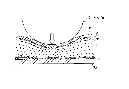
~igure 3 is a cross section of the information input sheet constructed
as above wherein a writing utensil, an input contact member or the like is pushed
against the input surface of the sheet. Elements
*trade-mark
- 7 -
''''` '
~3~6~7~7~7
1 designated by identical reference numerals to those
in Fig. 1 represent like elements, so the descripkion
thexefor is omitted. In Fig. 3, reference numeral
10 denotes the tip of a writing utensil or pen. As
seen from Fig. 3, upon application of a pen pressure
by the pen tip 10 to the information input sheet in
the direction indicated by an arrow, the laminated
flexible struc~ure deforms while the polyurethane
elastic layer 2 deforms with some of the spaces between
adjacent insulators being filled with the elastic
layer 2. Therefore, the conductive layer 1 coated
on the elastic layer 2 is pushed downward by the
deformed elastic layer 2 and contacts a partial area
of the resistive layer 6 ~hile embracing some of the
insulators within the area. Such deformation of the
elastic layer 2 is realized under the condition that
the thickness of the elastic layer 2 is set sub-
stantially the same as or greater than an average
distance between the edges of adjacent insulators 7,
and substantially the same as or greater than an
average length of bottom sides ~ of the insulators 7.
Since the shield layer 3 and -the protective film 5
are also flexible, the thickness of the elastic layer
2 may be considered as including the ~hicknesses of
the shield layer 3 and the protective film 5. If
the elastic layer 2 is made of a flexible layer
(elastomer) containing a conductive material such as
carbon, the conductive layer 1 needs not be provided.
-- 8
; , ~
- ~ , , .
~3~6~
1 The material of the dot type insulators 7 is selected
from those materials softer than that of the elastic
layer 2. Preferably, the soft nature of the material
is determined such that although the insulator 7 is
more or less crushed upon application of a pen pressure,
it deforms ~hile being pushed into the elastic layer
2 wlthout extending laterally. In this embodiment,
since the insulator 7 is deformed and crushed upon
application of a pen pressure, it helps the conductive
0 layer 1 contact the resistive layer more broadly,
which also results in an improved smoothness of
writing.
With the construction as above, the conductive
layer 1 can contact the resistive layer 6 upon appli-
cation o~ a pressure by a writing utensil of any tipthickness. Such contact may occur under too high a
pressure by a palm or a inger. However, assuming
that the ordinary pressure applied to the sheet when
a plam or a inger is placed thereon is substantially
the same as a pen pressure, the conductive layer 1
cannot contact the resistive layer 6 because the
pressure per unit area by the plam or finger is con-
siderably low as compared with that by the writing
utensil. Therefore, undesired input due to the touch
by a palm or finger can be avoided.
Figs. 4A to 4D show the contact state
between the conductive layer 1 and the resistive
layer 6 upon application of a pen pressure to the
_ g _
7~'7
1 information input shee-t of the above embodimen-t
according to the present invention. In Fiys. 4A to
4D, a black solid circle represents the insulator 7,
and a hatched portion represents a contact area
between the deformed conductive layer 1 and the
resistive layer 6. A difference between the contact
states of Figs. 4~ and 4B results from a different
thickness of a pen tip. A thinner pen is used in
Fiy. 4A than in Fig. 4B. Two hatched portions in
Fig. 4A indicate that a pen was pushed twice against
the sheet at two different positions. In both the
cases~ it can be understood that the conductive layer
1 is deformed by a pen pressure with some of the
spaces between insulators 7 being filled with the
elastic layer 2 and reliably contacts the resistive
layer 6 over a broad area. Fig. 4C shows the case
where a pen locates just upon one of the insulators
7. Also in this case, the elastic layer 2 is deformed
by a pen pressure and hence the conductive layer 1
is deformed to contact a partial area of the resistive
layer 6 while embracing some of a plurality of
insulators 7 within the area. Fig. 4D shows the
case where an insufficient pen pressure is applied
or a palm or finger touches the sheet. Xn this case,
the conductive layer 1 and the resistive layer 6 are
not allowed to contact each other.
Fig. 5 is a perspective view of an infor-
mation input board of a handwritten information input
-- 10 --
.
3L3~6~ '7
1 terminal to which the information input sheet a
this invention is applicable.
The information input sheet shown in Fig. 1
is represented by reference numeral 11 and is disposed
on the board with the protective film 5 facing upward.
An entry form sheet 12, various types of which may
be provided for different users, is placed on the
information input sheet 11. Necessary information
is depicted in the entry form sheet 12 with a pen 13
so that the information is supplied to the infor-
mation input sheet in the form of pen pressure. An
input information display 14 may use, e.g., a liquid
crystal display panel on which handwritten information
such as characters and symbols are displayed. The
information input board is connected to a control
unit 15 via a cable. The control unit 15 can recognize
handwritten information using a built-in CPU and store
the data in a memory, and supply power to the infor-
mation input sheet. The control unit 15 is coupled
to a host computer (not shown) to process the inputted
information.
- 11 -
..