Note: Descriptions are shown in the official language in which they were submitted.
~3~)7~S
T%REE TERMINAL REMOTELY CONTROLLED
SPDT ANTENNA 8WITCH
. . _
BRIEF DESCRIPTION OF THE DRAWINGS
Fiy. 1 i~ a ~che~atic diagram of a prior art,
four terminal, SPDT antenna ~witch.
Fig. 2 iB a schematic diagr~m of a prior art,
four terminal, transmit/receive switch.
Fig. 3 is a ~chematic diagram of the preferred
embodiment of the three ter~inal, SPDT antenna
~witch of the present invention.
Fig. 4 is 3 schematic diagram of an alternate
embod~ment of the three terminal, SPDT antenna
switch of the pre~ent invention.
BACRGROUND OP THE INvENrIoN
Thi~ invention pertains to antenna switches
and, rore particularly, to an antenna switch that
automatically switches 2rom a fir6t to a ~econd
antenna when the econd antenna i8 connected to the
~witch.
Fig. 1 i8 a schematic diagram of a prior art,
~our terminal, remotely controlled, cingle-pole
double-throw (SPDT) ant-nna switch 100. Radio
terminal R ~ connec~ed to th~ R~ input/output
terminal of a non-illustrated radio tran~ceiver.
Antenna terminal Al is connected to a rirst or local
antenna 101 while antenna terminal A2 i6 connected
to a ~econd or remote antenna 118. The DC voltage
at a 6eparate control terminal C determines whether
radio terminal R i~ coupled to antenna terminal Al
or A2.
q~
.~
13U~'15
-- 2 --
When the control voltage source 102 and,
consequently, the voltage at control terminal C are
a ground potential, a DC current flows from a source
of positive voltage V+ through resistor 104, RF
choke 106, diodes 108 and 110, and RF choke 112.
This current causes diodes 108 and 110 to switch to
the conducting state. When diode 110 is conducting,
capacitor 114 and inductor 116 form a parallel tuned
circuit which is anti-resonant at the operating
frequency. This anti-resonant parallel tuned
circuit decouples radio terminal R from antenna
terminal Al by inserting a high impedance in the
path between these two terminals. Since diode 108
is in the conducting state when control terminal C
is grounded, radio terminal R is coupled to antenna
terminal A2 through diode 108 and capacitors 120 and
122.
When the voltage at control voltage source 102
and control terminal C are at V+, no DC current
flows through diodes 108 and 110, and the diodes
switch to the open-circuit state. Since diode 108
is in the open-circuit state, radio terminal R is
decoupled from antenna terminal A2. When diode 110
i8 in the open-circuit state, capacitor 114 and
inductor 116 no longer form an anti-resonant
parallel tuned circuit. Consequently, radio
terminal R is coupled to antenna terminal Al through
inductor 116 and capacitors 120 and 124.
Fig. 2 i8 a ~chematic diagram of a prior art,
~our terminal, transmit/receive ("T/R") switch.
Transmit terminal TX is connected to the output of a
non-illustrated transmitter, and receive terminal RX
is coupled to the input of a non-illustrated
receiver. When the voltage at input control
s
-- 3 --
terminal C is suf~iciently above ground potential,
current flows through RF choke 202, diode 204,
quarter wavelength tran~mission line 206 and diode
208, thereby switching diodes 204 and 208 ~o the
5 conducting state. When diode 208 is conducting,
terminal 206A of transmission line 206 is shorted to
ground. This causes the impedance at the other
terminal 206B to go to infinity, thereby decoupling
antenna terminal A from receive terminal RX. Since
10 diode 204 is conducting, transmit terminal TX i5
coupled to terminal A and antenna 210 through
capacitor 212 and diode 204.
When the voltage at control terminal C is near
15 ground potential, no c:urrent flows through diodes
204 and 208. Consequently, diodes 204 and 208 are
switched to the open-circuit state. Thus, antenna
terminal A is coupled through transmission line 206
and capacitor 214 to receive terminal RX. Since
20 diode 204 i8 in the open-circuit state, transmit
terminal TX is decoupled from antenna terminal A.
The ~witches illustrated in Figs. 1 and 2 are
both SPDT RF type switches. In addition to the
25 three terminals o~ a conventional mechanical SPDT
switch, both prior art switches require an
additional control terminal C. Although the
invention described below also provides SPDT RF
switching, it has a distinct advantage in that the
30 separate control terminal C has been eliminated.
Thus, the invention only requires thrée terminals.
The invention has an additional advantage in that
switching f`rom a ~irst antenna to a second occurs
automatically, simply by connecting the second
35 antsnna to the switch.
7(~
- 4 -
SUMMARY OF THE INVENTION
BrieSly, the invention i8 a three terminal
antenna switch for use with a remote antenna ~ystem
that includes a remote antenna and a low pass filter
coupled to the remote ~ntenna. The 6witch includes
a radio terminal, ~nd firet and second ~ntenna
terminals. Means are included for coupling the
radio terminal to the first antenna terminal when
the second antenna terminal i6 unterminated. Me~ns
are al~o lncluded for coupling the radio ter~inal to
the ~econd ~ntenn~ terminal when the second antenna
terminal i6 coupled to the remote antenna. When the
remote antenna ByBtem i6 coupled to the 6econd
antenna terminal, ~C current flows through ~he
second antenna terminal.
In another mbodiment, the invention iB a
rcmote ant~nna ~witching sy~tem that includes a
throe terminal antenna ~witch and a remote antenna
system. The three terminal antenna switch includes
the element~ d~scribed ln the above paragraph. The
remoto antenna ~y6tem lncludes a remote antenna
couplod to a low pa6s ~ilter.
~ .
13~37C~5
-- 5 --
DESCRIPTION OF T~E PRE~ERRED EMBODIMENT
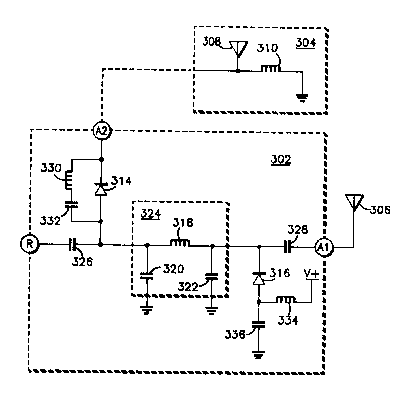
Fig. 3 is a ~chematic diagram of the preferred
embodiment of the three terminal antenna ~witch 302
and remote antenna ~yctem 304. An exemplary
embodiment of the invention of Fig. 3 that operates
in the 8~0 MHz band will be described. Those
skilled in the art will under~tand how to modify the
~xemplary ~mbodiment for operation at any other
frequency. Part ~alues for the exemplary embodiment
are l~sted in Table 1.
PART VALUE
Capacitors 326, 328 and 332 30 pico-Farads
Capacitors 320 and 3222.2 pico-Farads
Capacitor 336 10 pico-Farads
Inductor~ 310 and 334190 nano-Henrles
Inductor 318 9 nnno-~enries
Inductor 330 65 nano-Henries
TABLE
~ , .
13~'~7U~S
All capacitors are preferably ceramic chip
capacitors. Diodes 314 and 316 are preferably PIN
diodes, although other types may also be suitable,
particularly at low frequencies. PIN diodes are
preferred because of their low reversed bias
capacitance, which is typically a few tenths of a
pico-Farad. Conventional silicon diodes, however,
exhibit reversed biased capacitances on the ordPr of
tens of pico-Farads. Diodes 314 and 316 are
preferably Microwave Associates part no. MA4P739 PIN
diodes.
Referring to Fig. 3, antenna switch 302
includes a radio terminal R for connection to the RF
input/output terminal of a non-illustrated radio
transceiver, a first antenna terminal Al which is
connected to a first or local antenna 306, and a
second antenna terminal A2 which can be connected to
the remote antenna system 304. The second or remote
antenna system 304 includes a second or remote
antenna 308, and an RF choke 310. RF choke 310
functions as a low pass filter to permit the flow of
DC current from antenna terminal A2 to ground, while
providing a high impedance at radio ~requencies.
The term "remote" is used to describe the
second antenna system because, in the usual
application, the second antenna is positioned at a
greater distan~e ~rom the switch than the first or
"local" antenna. The physical separation of the
antennas from the switch, however, is not to be
construed as a limitation of the invention.
~L3V~7~'~S
- 7 -
Inductor 318 and capacitors 320 and 322 are
interconnected to form a lumped element equivalent
of a one-quarter wavelength transmission line 324.
A conventional one-quarter wavelength transmission
line would also be suitable.
When antenna terminal A2 is unterminated
(i.e., when remote antenna system 304 is not
connected to antenna terminal A2), no DC current
flows through diodes 314 and 316. Consequently,
diodes 314 and 316 are in the open-circuit state
and radio terminal R is coupled to antenna terminal
A1 through capacitor 326, transmission line 324 and
capacitor 328.
When diode 314 is in the open-circuit state,
it exhibits a small reverse bias capacitance that
can undesirably couple a small amount of radio
frequency energy between radio terminal R and
antenna terminal A2. To reduce the effect of this
coupling, inductor 330 forms a parallel tuned
circuit with the parasitic capacitance o~ diode 314.
This parallel tuned circuit i8 anti-resonant at the
operating frequency, thereby increasing the
impedance between radio terminal R and antenna
terminal A2. Capacitor 332 is a DC blocking
capacitor that also functions as an RF short at the
operating frequency.
When antenna terminal A2 i8 connected to
antenna system 304, DC current flows through RF
choke 334, diode 316, inductor 318, diode 314 and RF
choke 310. This causes diodes 314 and 316 to switch
to the conducting state. When diode 314 is
conducting, radio terminal R i8 coupled to antenna
terminal A2.
-- 8 --
When diode 316 is in the conducting state, it
exhibits a small amount of inductive reactance at
the operating fre~uency. Capacitor 336 forms a
series resonant circuit with the parasitic
inductance of diode 316, thereby reducing the
impedance between the cathode of diode 316 and
ground. It is well known in the art that if a one-
quarter wavelength transmission line is grounded at
one end, the driving point impedance at the other
end of the transmission line will be infinite.
Thus, when diode 316 is in the conducting state,
transmission line 324 provides a large impedance
between radio terminal R and antenna terminal Al,
thereby decoupling antenna terminal Al from radio
terminal R.
Thus, capacitors 326, 328 and 332, inductor
330, diode 314 and transmission line 324 provide a
means for coupling radio terminal R to antenna
terminal Al, provided antenna terminal A2 i6
unterminated. Similarly, capacitors 326 and 336,
inductor 334, diodes 314 and 316, and transmission
line 324 provide a means for coupling radio terminal
R to antenna terminal A2, providedl antenna terminal
2~ A2 i8 connected to remote antenna system 304.
A second embodiment of the invention i8
illustrated in Fig. 4. In this embodiment, the DC
bias current for diodes 314 and 316 is supplied by
the output of a DC amplifier 402. The input of
amplifier 402 is directly connected to antenna
terminal A2. When antenna terminal A2 is coupled to
remote antenna system 304, DC current flows from the
emitter of PNP transistor 404, through the base of
the transistor, resistor 408, antenna terminal A2,
13~7~'~5
and RF choke 310, and, finally, to ground. The
current in the base circuit of transistor 404 is
amplified at the collector, which supplies the bias
current to diodes 314 and 316 through ~F choke 406.
One advantage of the second embodiment is that the
DC current flowing through remote antenna system 304
and antenna terminal A2 is much less than that of
the first embodiment of Fig. 3. In fact, this D~
current can be made arbitrarily small by simply
increasing the gain of DC amplifier 402.
A third embodiment of the invention results
from a modification of Fig. 3. In this third
embodiment, diodes 314 and 316 are reversed (i.e.,
cathode to anode), inductor 334 is connected in
parallel with capacitor 336, and a DC voltage source
is inserted between inductor 310 and ground, the
negative terminal of the voltage source being
grounded. This embodiment functions in a manner
similar to the first embodiment illustrated in Fig.
3, but with two significant differences. First, DC
current flow~ through the circuit in the opposite
direction. In the first embodiment, DC current
flows out of antenna terminal A2 and into remote
antenna system 304, while, in this embodiment, it
flows from the remote antenna system and into
antenna terminal A2. Second, a voltage source is
required in the remote antenna system 304.
Although switching from one antenna to the
other may be accomplished, as before, by connecting
and disconnecting the remote antenna system to
antenna terminal A2, this embodiment permits an
additional method of switch control. Specifically,
if remote antenna system 304 is
13~7~i~5
- 10 -
connected to antenna terminal A2, switching from
antenna terminal Al to A2 may be accomplished by
varying the voltage of the remote DC voltage source.
When this DC voltage is set at a level sufficient to
overcome the forward voltage drop of diodes 314 and
316, radio terminal R will be coupled to antenna
terminal A2. If the DC voltage is set below this
level, radio te~minal R will be coupled to antenna
terminal Al. A disadvantage of this third
embodiment, however, is that it may be impractical
to place a DC voltage source in the remote antenna
system.
A fourth embodiment results from a similar
modification of Fig. 4. A D~ voltage source is
included in remote antenna system 304, diodes 314
and 316 are reversed, RF choke 334 is connected to
V+ as illustrated in Fig. 3, and an NPN transistor
is substituted for PNP transistor 404 with its
emitter connected to ground. This fourth embodiment
permits switch control by the connection and
disconnection of remote antenna system 304 to
antenna terminal A2, or by altering the DC voltage
of the remote voltage source as described above.
Other variations of these four embodiments
could also be constructed using conventional
electro-mechanical relays. For example, a variation
of the embodiment of Fig. 3 would include a SPDT
relay wherein the common terminal is connected to
radio terminal R, the normally closed terminal
connected to antenna terminal A1, and the normally
open terminal connected to antenna terminal A2. One
terminal of the relay coil would be coupled to
antenna terminal A2 through an RF choke, while the
other coil terminal would be connected to a source
of positive voltage.