Note: Descriptions are shown in the official language in which they were submitted.
1307056
~11 CKtlES S /DENS I TY MEAS UR I NG APPARATUS
Back~round of the Invention
1. Field of the Invention
The present invention relates to a thickness or densitv
measuring app~ratus which is particularly adapted to measure the
thickness or density Or a film. The invention has particular,
though not exclusive~ utility in the plastics processing industry
where thickness and/or density of an extruded plastic film must
be controlled to production tolerances.
2. Description of the Prior Art
Thickness and/or density measuring systems are known in
the art which rely on various types of sensors for a measure-
ment. ~or thickness measurements, mechanical g~uge-type devices
are known which contact with the material or ob~ect to be mea-
sured and which provide a thickness readout which can be used to
control apparatus for manu~acturing the material and/or ob~ect to
insure that a desire thickness is obtained. Likewise, densitv
measuring devices are known in which the density of an ob~ect is
l l
~.,
! ~3~ r~
measured usually by pnssing radiation throu~h the object.
Changes in density are seen by ch~nges in the transmittance of
the radiation through the object.
In m~ny production environments particularly where
plastic films and sheets are being manufactured, the control over
material usage and quality of the product is greatly enhanced
when the thickness of the material can be accurately measured.
This is especially true when the measurement can be made in an
on-line manner where the measurement instrument can be installed
on or quite close to the producing n~chinery and the thickness
information can be used in a feedback control system for the
process so that optimum parameters can be determined for the
machlnery to produce a desired film product. In such an environ-
ment the output of the measuring instrument must respond auickly
to thickness variations, and the output is fed back electron-
Ically or mechanically to control machinery without any human
Interventlon. In order to do thls, the instrument must be in-
herently rugged to wlthstand the harshness ot the production
envlronment, be ~mall enough In size to be able to flt where the
measurement 18 most needed, and have minimal input and output
connectlons 80 that integratlon with computing and control equip-
ment can be facilitated.
At present, many thickness measurements are made using
the prlnciples of detectlon of nuclear and atomlc partlcle-radi~-
tlon emltted from a source. U.S. Patent No. 4,047,029 is repre-
sentat~ve and dlscusses varlous radlatlon sources Includlng those
producing beta particles, X-rays and ~amma rays. These rays are
- 2 -
~ 13C~ 6
¦sttenuated or scattered when they pass through 8 m~terial as e
¦consequence of their interaction with the atoms and nuclei in the
¦material. The amount of interaction is dependent on the number
¦of atoms and nuclei in the path of the radiation and the tendency
¦of the m~terial ~o interact with the type o~ radiation striking
¦ it. ~or a given material and type of radiation the amount of
interaction will depend on the material's density snd thickness
since density determines the number of atoms and nu¢lei in the
path of the radiation per unit volume and thickness determines
the length of the travel when the radiation is made to pass
through the material, usually at right angles to a flat surfaee.
Present generation thickness measuring devices based on
the principles of particle detection will detect and-count in-
dividually particles that pass through a sample of a material and
compare the count rate observed for an unknown sample with Q
count rate observed with a sample of known thickness. The mater-
lal thickness i8 then Interred by assuming similar density be-
tween the known and unknown samples and applying, typically, a
linear relationship between the count rate and material thick-
ness. The relationship is typlcally not linear over a very large
range but cQn usually be assumed to be linear over the range of
thicknesses encountered in a production environrnent, without
signi-icant loss ot accuracy~
The method currently employed tor detecting such radia-
tlon works through the use Or a scintillation detector or a gas
tilled ionization counter. The ionization counter consists ot a
chamber of gas which can be made to ionize by the radiation and
the resulting electric charge is collected through the use of a
high voltage between the chamber wall and a thin wire in the
~ 13C~'7~
¦center of the chamber. Ionized pairs of electrons and atoms are
¦drawn to the opposite polarity, which will be the wall or the
¦wire, depending how the voltage is applied, under the influence
¦of the resulting electric field. This charge is then collected
and amplified as a signal in a charge sensitive amplifier and
then may be compared to a voltage threshold to determine whether
a valid detection has been n~de. A disadvantage of an ionization
chamber in a production environment is th~t the gas may leak out
of the chamber or may break down and degrade through use and the
chamber is usually quite large to achieve efficiency, making it
difficult to apply to many environments. Moreover, the ioniza
tion chamber requires a very high voltage, typically in the range
of 1,000 to 3,000 volts, and is alss costly which further in-
hibits its widespread use as a thickness measuring device.
The scintillation detectot, which is also known in the
art to measure thickness, uses a material called a scintillator,
which when it absorbs a unit of radiation becomes activated and
wlll deactivate by giving off light in the ultraviolet range
through the proces8 of scintillation. This ultraviolet light is
then detected by a quite sensitive light detector known as a
photomultiplicr tube. The Dhotomultiplier tube is closely
coupled to the sCintillator material so that ultraviolet light
will pass into it. A detection signal ~rom a ~irst photocathode
within the photomultiplier tube is typically multiplied by a
8erie8 of dynode ~tages which are successively more positive in
charge than the preceding dynode stage. The multiplied signal is
then taken as an output signal. A disadvantage o~ the scintilla-
tion detector is that it also uses lethal high voltages in the
- 1 13(~ 6
l,000 to 3,000 volt range and in addition the photomultiplier
tube characteristics change and dri~t with use and age and with
fluctuations in the high voltage level. This type of a deteetor
is also prone to breakage since it is an evacuated glass tube snd
because of its size, weight and cost this type Or detector also
cannot be used in many types of environments.
Semiconductor diode pasrticle dete~tors are also known.
They consist of a p-type layer, an n-type layer and an optional
intrinsic layer in the middle. This diode is sensitive to light
and nuclear and atomic radiation when the same strikes the diode.
Detectors of this type have been used for high resolution nuclear
spectroscopy. The signal generated by this type of detector
consists of the collection of charge relessed when the r&diation
loses energy in the sensitive region of the detector. This
charge is collected across the p-type a~d n-type materials and is
amplified with a high performance charge sensitive amplifier.
Typically these types of detection devices have a very
small output signal. The output signal is so small that noise
generated by thermal ef-ects or impuritles and imperfections in
the silicon materi81 wlll overcome the charge 8ignal. ~or this
reason, 8uch detectors are typically operated at quite low tem-
perature8, usually through the use of a liquid nitrogen coolant
to arrive at adequate performance. While thls type of detector
could be used in laboratory research, It cannot be practically
used In a production environment.
,
I 13(~r~
Summary of the Invention
One object of the invention is the provision of a small
compact, rugged and low cost particle radiation detecting thick-
ness/density measuring system.
Another object of the invention is the provision of a
particle radistion detecting thickness/density measuring system
which operates on low voltages.
Another object of the invention is the provision of 8
particle radiation detecting thickness/density measuring device
which can have separable parts, one including a detection head
containing those elements necessary for detecting and registering
particle counts and another processing and display section
located elsewhere for monitoring the thickness measurement with a
simple low voltage cable passing between the two.
An additional object of the invention is the provision
ot a portable low-cost particle radiation detecting thickness/
density measùring apparatus which provides a fixed gap between a
radlstion source and detection head in whlch a materlsl of un-
known thickness can be placed tor measurement.
Another ob~ect o- the invention is the provision ot a
control 3ystem tor monitoring and controlling the thickness of an
extruded tilm during its production uslng Q plurality ot simple,
low cost particle radiQtion detecting thickness measuring de-
vices.
The present invention m~kes particular use of a new
type ot silicon diode detector which contains a p-layer, an n-
layer and an intrinsic layer between them and which is operable
at room temperature to detect radiation. The device, termed a
PIN diode, is primarily intended for detection of laser and
- 6 - i'
~ 1307C~
ultraviolet light, but it has also been discovered thQt this¦
detector is also sensitive to nuclear snd atomic radiation such
as beta particles, X-rays and gamma rays.
The invention employs the PIN diode in ~ pQrtiCul~r
mechanical ~nd circuit configur~tion to enhance its ~bili~y to
detect particle radiation only. A light blocking window is used
to screen the PIN diode from the effects of light radiation while
the output signal therefrom is connected to a charge sensitive
preamplifier. A high quality amplifier is then connected to the
output of the preamplifier to develop a suitable signal which can
be provided to a threshold detector, the output of which is sent
to a pulse rate counter. The output of the pulse rate counterj
can be used together with pulse rate information derived during
previous calibration use o~ the invention for a material of known
thlckness to determine a thickness measurement from a detected
pulse rate when a material of un~nown thickness is provided in
the Path Or the radiation ~rom a source to the PIN diode detec-
tor. Slmllar callbration and detectlon steps can be used to
employ the Inventlon a8 a denslty mea8ur~ng devlce.
By uslng a PIN dlode and assoclated small scale elec-
tronlcs package, a 8mall compact detector can be provlded which
wlll 8110w It to be used In many appllcatlons that present gene-
ration thlcknéss mea8uring devlces based on the principle of
psrtlcle radlQtlon csnnot approach. Typlcally, such a detector
could be used in profile extruslon, blown ~llm 8nd blow molding,
as well as the typlcal areas such as sheet and rllm extruslon.
Moreover, slnce the measurement Instrument o~ the inventlon re-
quires only low voltage circuits, there Is no sarety ha2srd and
- 7 -
13~ 6
associated heavily insulated power cables and connections are
svoided thereby opening up new installation possibilites over
present day equipment. Still further, the small size and compact
solid state construction can provide high reliability and
stability, while minimizing the possibility of damage of breakage
Or glass tubes or gas chambers typicfllly associated with prior
art devices. Fewer calibration oper~tions and fewer repairs are
also attendant the construction. Finally, because of its compact
size, solid stage cons~ruction and use of relatively low cost
components, the detector can be manufactured at lower cost than
present generation thickness measurement systems.
Because of its low cost and oompact construction, a
plurality o- measuring devices can be arrayed across an extruded
rilm to mea~ure the material thickness simultaneously across its
width at discrete points. Because of the complexity and size of
present generation equipment, this approach cannot now be
achleved, and instead mechanical scanning of a thickness measur-
ing device acros3 the width o~ a sheet must be employed which has
undesired complexity due to the mechanical scanning mechanism.
Each o~ the plurality o~ thickness measuring devices provided in
the array can then be used to control a respective section of
processing machinery such as respective lip sections of an extru-
sion die to control the extruded product to desired specifica-
tions.
The above and otheP ob~ects, advantages and features Or
the invention will be more readily understood rrom the rollowing
detailed description o~ the invention which is provided in con-
nection with the accompanying drawings.
- 8 -
13~ 56
Brief Description of the Drawings
Fig. I illustrates in electrical block and schematic
form a first embodiment of the present invention;
Fig. a illustrates in flow chart form a microprocessor
program for a method of calibrating and measuring an unknown
thickness using the embodiment showm in Fig. l;
Fig. 3 illustrates in ~low chart form a microprocessor
program for snother method of calibrating and measuring an un-
known thickness;
Fig. 4 illustrates a modification of the Fig. 1 embodi-
ment showing a different way of mounting a particle radiation
detector;
~ ig. 5 illustrates another dification of the Fig. I
embodiment;
Fig. 6 illustrates a modification of the Fig. 4 embodi-
ment;
Fig. 7 illustrates another modification of the Fig. I
embodiment using a back-scatter radiation technique;
Pig. 8 illustrates a control system for an extrusion
die utilizlng the present invention;
Fig. 9 illustrates an array Or thickness measuring
detectors for use in a control sy~tem or controlling the thick-
nes~ Or an extruded r ilm;
Pig. 10 illustrates in tlow chart form a microprocessor
program for a method Or calibrating and measuring an unknown
density using the embodiment shown in Fig. l; and
Fig. 11 illustrates in flow chart form a microprocessor
program for another method of calibrating and measuring an un-
known density.
3~
Detailed Description of the Invention
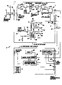
Fig. I illustrates the thickness/density measuring
system of the invention in partly schematic, partly block dihgram
form. The thickness/density measuring system 7 is constructed in
two component parts identified in Pig. l as detector head section
ll and processor and display section l3. These sections are
interconnected by a low-voltage csble 37 and are described more
fully below.
Detection head section ll includes the detecting elec-
tronics for a thickness/density measurement, while processor and
display section 13 contains the processing and display components
for providing a digital display of a thicknessldensity measure-
ment and/or an output signal representative of the thickness/
density measurement which can be used ~or control purposes.
Turning now to the detector head section 11, it in-
cludes a window 19 in the housing which blocks entry of light
radiation into the houslng, but which permits particle radiation
to pa~s therethrough. Suitable materials which can be used for
wlndow 19 include alurninized mylar. Dlsposed behind window 19
and within housing 11 is a PIN diode 21 which 18 sensitive to
radiation, both llght radiation and particle radiation. As
noted, wlndow 19 i8 impervious to 11ght radiation 80 that PIN
detector 21 can only detect particle radiation such as ~-rays,
beta rays and gamma rays. This particle radiation is emitted by
a radiation source 15 whlch is spaced from window 19. The mater-
ial 17 to be measured Is placed between the radiation source 15
and window 19.
The output of PIN diode 21 is connected to a charge
sensitive preamplifier 23 the output of which is connected to a
first high pass filter 25. The output of the high pass filter 25
-10-
! 13C~ r~
is in turn psssed to the input of a low noise operational ampli-
fier 27, the output of which then passes through e second high
pass filter 29. The output of the high pass fi1ter 29 represents
voltage pulses which correspond to charges which are detected by
the PIN diode 21. The output of the high pass filter 29 is con-
nected to the input of a comparator 31 which has a threshold set
by resistive network 33 applied to another input thereof. The
high pass filters block low frequency noise components while the
threshold of comparator 31 is set so that miscellaneous noise
which does not constitute a valid detection pulse will not affect
the readings of the instrument. W~en the output of the high p~ss
filter 29 exceeds the set threshold the comparator 3l provides an
output pulse which i$ then fed to an opto-isolation and line
driver circuit 35. The output of the isolation circuit 35 is
then connected to a terminal strip on the detector head section
ll for connection with additional processing electronics in the
dlgital processlng and display section l3.
Before descrlbing the digital processing and display
section 13, the remainder of the circuitry provided in the de-
tector head section ll wlll be descrlbed. In order to provide
operative power to the various electronic components within the
detector head section ll, a power supply Is built therein. Be-
cause the PIN diode requires different voltages than other elec-
tronic components within the detector head asse~bly, a multivolt-
age power supply Is provlded in the orm o- a transformer 39
having a plurality o- prlmary windings 4l and 43 and 8 plUrQlity
of secondary windings 45, 47 and 49. The secondary wlndings are
- 1 1
13~t-`'6
¦connected to respective diode/capacitor networks snd provide the
¦operating D.C. voltages required for the various circuit compo-
nents within the detector head section 11. One side of primsry
winding 41 is connected to receive an unregulated input voltage
applied to an input terminal strip 36 at the detector head sec-
tion 11 And received frcm the digital processing and display
section 13. This unregulated voltage supply is switched by 8
trnnsistor switching device 42 under control of a pulse width
modulator 53 Pulse width n~dulator 53 also receives a D.C.
voltage input from a primary reference winding 43 through a diode
capacitor network such that the pulse width m~dulator 53, network
51 and switching device 4a as well as the primary winding connee-
tions runction to provide a regulated voltage output at the
secondary terminals 46, 48 and 50.
An important aspect or the present invention is that
the detector head section 11 can be made of very small size and
the power supply ~or the detector head operates on low D.C. volt-
age~ which makes the detector head suitable ror placement in many
environment~ wherein high voltages and/or bulky and comple~
equipment cannot be provided.
The dlgital processing and display section 13 provldes
a low voltage power supply input to the detector head 11 and sup-
plies this via a power supply circuit 57 which receives an A.C.
power input 67. Alternatively, a D.C. power source can be pro-
vided. The digital processing and display section 13 ~urther
includes a tlmer 59 whlch de~ines time windows during which a
digital pulse counter Bl is enabled to count pulses which sre
- l2 -
13C~7~6
received from the output Or the opto-isolation circuit 35 in the
detector head section 11. The pulse counter 61 is gated by the
timer 59 to establish a pulse rate counting circuit which pro-
vides a count pulse tor a given period of time. The output o~
the digital pulse counter 61 is in turn gated into a micropro-
cessor 63 whlch includes the usual RCM and RAM memory circuits
~or ~toring prograrns and data. A manually operable panel input
service 71, containing a plurality or input switches or keys and
input setting devices, is also provided for providing input
information to the microprocessor 63. The microprocessor also
provides as output signals a digital signal on terminals 69
representing a thickness or density measurement and an output
signal to a digltal display 65 provided wlthin the digital pro-
cessing and display section 13 also representing a thickness or
densitg measurement.
At this point it should be noted that the first embodi-
ment o- the invention can be used tor either a thickness or a
density messurement, depending on the programming ot micropro-
¢essor 63 as wlll be more tully descrlbed below.
Microprocessor 63 contains an algorithm for calculating
a th{ckness or density measurement based on the count rate it
recel~es ~rom the digltal pulse counter 61. It is ~irst neces-
sary to callbrate mlcroprocessor 63 with reterence data corre-
sponding to reterence data which indicates a known thickness or
dens1ty and a measured count rate tor that known thickness or
denslty 80 that later measurements can be related to this cali-
bration standard. The calibration rOt and measurement or an
unknown thickness o~ a tilm will tirst be described.
- 13 -
13~ cr!r;~
¦ Pig. 2 illustrates in flow chart form the programming
¦or microprocessor 63 which enables it both to be calibrated in
¦ the first instance and then to tAke thickness measurements there-
after. The operation depicted in Fig. 2 is based on a two sample
cslibration technique. In a first step 101 o~ the processing, a
switch on the front panel input device 71 o~ Fig~ 1 is read to
determine whether a calibration or a measuring operation is de-
sired. In step 103 the microprocessor determines which type of
processing is required. If a calibration procedure is selected
by the front panel input devices 71, the microprocessor proceeds
to step lOS where it displays on the digital display 65 a prompt
to an operator instructing him to insert a reference sample into
the measuring path between source 15 and window 19. In addition,
the mlcroprocessor further reads a thickness setting Input de-
vlce, e.g., digital value switches, on the front panel input
device 71 to obtain a signal representing an actual thickness Tl
ot this sample. Following step ;07 the microprocessor proceeds
to step 109 where It measures the count rate Cl, for the sample
ot known thlckness In ~tep 109. Pollowlng thls the micropro-
cessor actlvates the dlgital dl8pla~ fi5 to prompt an operator to
place a 8econd sample o~ known thlckness between the radiation
80urce 15 and wlndow 19. In addition, the microproces~or re-
celves as 8n Input on ~ront panel Input device 71 an entered
thickness T2 correspondlng to the second sample. Thereafter, the
mlcroproce8sor proCeeds to step 115 and mea8ures the count rate
Ca for the second sample and after thls proceeds to step 117
where It computes a slope M value using the equation:
M = (T2-Tl)/(C2-Cl) (')
Followlng this, the microprocessor proceeds to step 119 where it
calculates an intercept value 8 as
::3L3~t~ 6
B = Tl-(M x Cl) (2)
IThe slope value M and intercept value B Qre then ~tored in step
¦121 for later use by the instrument in calculating thickness of a
¦sample of unknown thickness.
¦ Returning to step 103, if an actuAl measurement is
¦desired, the microprocessor proceeds from step 103 to 123 where
¦it measures a count Cu rate for a sample of unknown thickness.
Thereafter it computes an actual thlckness Tu using the equation
u = (M x Cu) + B (3)
where M and B are the values previously obtained in the calibra-
tion step. This yields a thickness measurement which is then
displayed on digital display 65 in step 127 or alternatively
output to control equipment on lines 69 of the digitnl processing
and di~play unit 13.
Fig. 3 shows an alternate thickness calibration and
measurement program which can be used with the microprocessor
63. In this processing sequence, a single calibration sample is
used to calibrate the instrument. In a first step 201 the front
panel Input device 71 i8 read to determlne whether a calibration,
a measurement, or a material type entry routine is to be e~e-
cuted. I~ the rront panel swltch at input device 71 indicates a
cal~bration routine i8 desired, step 203 causes retrleval and
execution o~ the calibration subroutine. The microprocessor thus
proceeds to step 205 where it prompts an operator on the digital
display 65 to insert a cal~bration sample between the radiation
source 15 and wlndow 19. In addition, a thickness Ts of the
materlal sample is input at step 207 on the front panel input
15 _
~ ~3U7~6
¦device 71 and following this step the microprocessor proceeds to
¦step 209 where it measures a count rate Cs. It then records the
¦measured count rate Cs and the inserted sample $hickness Ts in
¦step 211 and proceeds back to step 201. With the Fig. 3 calibra-
¦tion technique, a m~terial type entry, e.g., polyester, nylon,
¦acrylic, etc. must also be made at input device 71. W~en the
material type entry is indicated on the front panel input device
71, the microprocessor 63 senses this in step 203 and then
branches to step 223 where it displavs a prompt on the digital
dlsplay 65 for an operator to enter, via the front panel input
device 71, a matçrial type which is used in the calibration.
Material type as set in the front panel input device 71 is then
read by the microprocessor 63 in step 225 recorded and stored in
step 227. All the data reguired for the microprocessor now to
calibrate itself for making an actual measurement of the material
thickness is present. Thus, when the ~ront panel input device 71
ls now set for a measurement, step 203 executed by the micropro-
ces~or will cause a measurement routine to be started at qtep 213
where the count rate Cu of an unknown sample p]aced between the
source 15 and window 19 is taken. After this, in step 215, the
values C8 and T8 obtained durlng the calibration routine are
retrleved ~ollowing which, in step 217, an M value is obtained
based on a table stored in the microprocessor ~nterrelating the
count values C8, the set thickness T8 and the inserted material
type. This table is a stored lookup table and contains various
values of M based on various combinations o~ values of Cs, Ts and
material type. ~ollowing step 217, where the value M is obtained
- 16 -
l3~tJ6
from the lookup, a thickness computation is made in step 219
based on the ~ormula
Tu = (~ x (Cu-Cs)) + Tg (4)
The thickness value is then displayed in step 221 on displsy 6
or output on lines 69 to further processing or control apparatus,
following which the microprocessor proceeds back t~ the beginning
of the program.
The calibration techniques described in Figs. 2 and 3
have their respective advantages and disadvantages. The cali-
bration technique of Fig. 2 is straightforward and requires only
operator entry of known thickness values, but requires two
ssmples of dif~erent known thicknesses for calibration. While it
provides a very good cs~ibration of the instrument, the require-
ment of having two samples of close, but measurably different
thickness, may be di-ficult at times and sometimes even impos-
sible to achieve. Consequently, the Pig. 3 calibration tech-
nique, which i8 somewhat more cumbersome to execute, requires
only one sample, has that as one beneflt. The theory on which
the calibration ot Pig. 3 Is based i8 that a p~rticulsr count
rate observed under any given circumstances will be etfected by a
number o- tactors including source strength, source to detector
separation and geometry, losses in the detector window, dirt
accumulatlon on the detector window, electronic sensitivity snd
threshold setting, flnd, o- course, rnaterial compositlon and
thickness. A single calibration sample observ~tion will estab-
lish the net result of the combination of these parameters st a
particular point in time. In production use, the only varlable
- 17 -
~ ~3Cl'76~6
¦of practicsl concern is the unknown m~teriel thickness for a
¦reasonable period of time. A reasonsble period o- time is estab-
¦lished by such factors as a half life of a radioactive source
¦which typically would be quite long compared to a production
period, the drift rate of the electronics, snd the rate of accum-
ulation of dirt on the window. The ~ig. 3 calibration technique
is based on the fsct that once a count rate has been established
for a given thickness of a type of material under a certain con-
dition of source strength, source to detector separation etc.,
the variation and count rate with material thickness represented
by M in Equation 4 above, can be predetermined and stored per-
manently in the device for use during production measurements.
Since ~ wlll be somewhat dependent on the nominal count rate and
type o~ material being measured, a number of values of M can be
predetermined and stored in the microprocessor 63 and an M can be
selected by microprocessor 63 which most closely matches the
operating conditions. The materisl type is thus operator select-
able through the ~ront panel input device 71 and the nominal
count rate can be taken during a callbratlon sQmple count so that
the microprocessor 63 can then make sppropriate selection of the
value M. To determine the initial values Or M which can be per-
msnently stored in the microprocessor 63 repeated application o~
Equation 1 abo~e can be used over a range of material types and
thicknesses. These results can be arranged in a tabular rorm so
that when a partlcu~ar callbration sample thickness and material
type are entered and the count rate observed, the value of M
which most closely matches these conditions can be selected for
use.
- 18 -
~ 13~ ;J6
In summary, the calibration technique Jllustrated in
Fig 3 has the advantage that a single sample of production
material, manually measured for thickness, can be used as the
calibration sample and to establish the nominal count rate of
production for the algorithm to select a proper value of M for
later thickness measurements. A single step calibrstion pro-
cedure is thus provided which is more readily used by unskilled
operators.
Fi~. 4 illustrates a modification of the detector head
11 illustrated in Fig. 1. In this embodiment, an easily remov-
able detector hesd assembly is provided which can be readilv
fixed to production machinery. The PIN diode 21 is shown bonded
by an Epoxy 305 or similar adhesive to the inner periphery of an
exteriorly threaded sleeve 303. An aluminized mylar entrance
window in the orm of a film 309 is provided at one end of the
threaded sleeve 303 with an O-ring seal 313 being provided be-
tween the mylar wlndow and an end of threaded sleeve 303.
locklng c8p 301 is threaded onto the outer periphery of threaded
~leeve 303 whloh serves to hold the mylar fllm 309 In place and
whlch al80 serves to provlde a backstop whlch limits the ~mount
of travel Or the threaded sleeve Into an openlng in the section
11. Cap 301 includes an openlng 302 at a ront 9ide thereof at a
position corre8ponding to the locatlon of the mylar wlndow 309.
A backlng nut 311 is screwed onto the threaded shaft 303 behind a
wall of the detector head hou81ng 11 to hold the entire detector
hefld In place. The leads of the PIN diode 21 are then affixed to
;~ _19_
I 13C~'7~6
an electronic circuit board containing the remainder of the elec-
tronics o~ the detector head assembly shown in Fig. 1. The de-
sign of the housing illustrated in Fig. 4 is particularly advan-
tageous as it allows ready replacement of the actual detector
head itself, ineluding the PIN diode, without requiring a com-
plete disassembly of the components within housing 13.
The aluminized mylar window 19 and 309 illustrated in
Figs. l and 4 can be formed of a mylar fiIm having Q thickness of
0.5 to 5.0 mils. The window can also be made of a thin aluminum
or stainless steel roil. In addition, the PIN diode illustrated
in Figs. 1 and 4 is a windowless construction wherein protective
layers covering the active PIN areas are not provided by the
manu~acturer to maximize radiation sensitivity. Thus, the mylar
window 19 or 309 provides the principal form of protection for
PIN diode 21. Mylar window 309 of Fig. 4 contains the same alum-
inized construction as Pig. 1 which blocks light Padiation from
striking the PIN diode 21, thereby improving reliability of de-
tection o- particle radiation.
In the embodiments o- the invention thus described, the
radiation source, which may emit gamms rays, X-rays, or beta
rays, 18 ixedly spaced ~rom the detector head sectlon 11 by
being mounted on a separate support. It is also possible to
provlde an integral supPort on the detector head section ll for
the detector source which would then provide a ~ixed gap between
the source and PIN detector within which a materlal whose thick-
ness is to be measured can be placed. This embodlment is illus-
trated in greater detail in ~igs. 5 and 6 which respectively
correspond to the embodiments o~ Figs. I and 4, but with an ex-
tension arm 313 integrally connected to section ll and extending
13C1 7~ r ~ I
therefrom in a L-shape ~sshion to provide Q gap between the rad-
iation source snd radiation detector. With this integral con-
struction, it is possible to construct the entire detector unit
as a simple portable assembly. Moreover, since the detector unit¦
operates on low voltages, it is further possible to incorporate
all of the electronics including those of the digital processing
and unit provided in section 13 Or Pig. I into a single housing
which is readily portable to different environments of use.
Fig. 7 illustrates a modification of the invention
whereln the detector head section 11' is used in a backscatter
radiation detection technique. In this embodiment, the PIN diode
21 is mounted within a relatively thick material portion of one
end o- the section 11. In addition, the radiation source lS' is
Qlso mounted in the same end Or the housing but the housing is
con~igured so that most, ir not all, of the radiation from source
IS pro~ects outwardly of the housing and not directly toward the
PIN dlode 21. A8 a consequence, a material can be stretched
8cro88 the one end o- the aection 11 in tront of the radlation
~our¢e lS 8nd PIN diode 21, Qnd bsck~cstter r8distion c8n be
detected ~rom the scurce by the PIN diode. The arnount Or baek-
sc8ttering which occurs will be dependent on material thickness
8nd thu8 the In8trument can be cali8br8ted or radi8tion count
bssed on backscatter u8ing either o~ the calibration techniques
described Qbove with respect to Pigs. 2 and 3. In the Pig. 7
embodIment, the PIN diode l8 mounted in a PIN diode holder 26
which has external screw threads which screw with a threaded bore
as provided in one end o~ the detector hesd section 11.
- 21 -
1 13V7~'~6
¦ The only difference between the microprocessor 63 pro-
¦ gramming for calculating a thickness value when the backscatter
¦ approach is used is that the numerical sign o~ the slope constant
¦ M will evaluate to be positive when the calibration procedure is
followed. This is due to the fact that the count rate increases
for increasing material thickness in the backsc~tter mode while
it decre~ses for increasing material thickness in a transmission
mode.
Figs. 8 and 9 illustrate a control system with which
the thickness measuring device 7 of the invention can be partic-
ularly suitably employed. The control system is used to control
sections of die lips o~ a film extrusion system. Fig. 8 is a
slde view o~ the system which includes an extruder barrel 401
supplying a plasticized material to a die 403 for e~truding a
thin sheet o~ plastic material. Die 403 includes die lips 405 at
the outlet end thereof which are adjustable with respect to the
gBp de~ined b9 the IJps to thereby adjust the thickness Or the
materlal leaving the die. Typically, a bolt 407 i8 used to ad-
~ust the dle llps with manual operatlon or the bolt belng used to
et~ect a coar8e ad~ustment and wlth a system providlng a ~ine
ad~ustment Or the gap between the die llps. In many Instances,
the ine ad~ustment is provided by actually heatlng the bolt 407
to provide rine ad~ustment Or the die gap. This heating is con-
trolled by a control system 413 whlch includes a typlcal PID
(proportlonal, Integral, derlvatlve) controller whlch in turn is
connected to the output o~ the thickness measurlng devlce 7
Illustrated in Fig. 1, partlcularly to the output provided at
terminals B9. Film 411 which passes ~rom the dle lips is taken
- 22 -
'.~
13~7G~t~
over a haul-off roller 409. In order to meflsure thickness, A
r~diation source 15 is provided on one side of the film and the
detector, including housing sections 11 and 13 are provided on
the other side of the film. Alternatively, a backscatter tech-
nique may be employed as illustrated in Fig. 7. In either event,
the output signal of the thickness measuring device is applied to
the PID controller 413 to in turn control the heating of bolt 407
which finely controls the gap of die lips 405. As illustrated in
Fig. 9, for a sheet of substantial width, the die lips 405 sre
divided into a plurality of die lip sections 405a...405f, with
each being controlled by respective die bolts 407a...407f and
w{th the heating of each die bolt being in turn controlled by a
respertive PID controller 413a...413f. The inputs to e~ch of
these controllers are respectively derived from individual thick-
ness measuring devices 7a...7f constructed as described above.
With this arrangement, each measuring device 7 measures a portion
of the width-wise extent of the film 411 and in turn controls
Indiv1dually its own heater bolt 407 so that the thickness of
each ~ection of the width-wise dimen9ion of the film is individ-
ually and sepQrately controlled.
Thus far, the Invention has principally been described
with reference to thickness measurements. However, it is also
po8sible to usé the same apparatus for measurin~ density. To
allow density measurement, three conditions must occur, the
thickness of a material placed between the source and detector
must remain constant, or the material completely fills the volume
between the source and detector as in a fluld medium, or the
thickness is known and fed into an algorithm by an external
- 23 -
~ ~3~7~:6
¦thickness n~asuring device which can then calculste a density
¦fr~m the messured thickness and known materi~l characteristics.
Fig. 10 shows a modification of the Fig. 2 flow chart
to permit use of the Pig. 1 apparatus for a density measurement.
As shown therein, step 107 is modified as new step 107', step 113
is modi~ied ss new step 113', and steps 117, 1!9 and 125 are all
modified as new steps 117', 119' and 125'.
Without describing again all of the steps illustrated
in Fig. 2 which are common in Pig. 10, those steps which are
common hsve the same reference numbers. Those steps which are
changed are designated by a prime (') symbol. In step 107' of
~ig. 10, a density Dl is entered for a first material sample
while in step 113' a density D2 is entered or a second material
s~mp1e. In step 117', the slope M i~ computed using the formula
M = (D2-Dl)/(C2 Cl)
In step 119', the intercept is computed ss
B = Dl-(M x Cl) (6)
Wlth the now stored calibrst~on values o~ M snd B, a density
measurement can then be carrled out, with the density computstion
made In step 125' 8S
Du = (M ~ Cu) + B (7)
Pig. 11 illustrates the modi~icstions needed ror the
Flg. 3 ~low chart to attain a density messurement.
In the csllbration technlque tor density measurement
Illustrsted in Flg. 11, an Input ssmple density i8 input to the
sy~tem in step 207' snd this together with a delected count rste
- 24 -
~ ~3C~7(~6
¦Cs for the sample is recorded at step 211'. A s~mple nuterial
¦type is also entered snd stored at step 227. Pinally, to calcu-
¦late R density measurement, a measured count rate Cu at step 213
is first taken following which values Cs and Ds entered during
the calibration sequence are used eO obtain a slope value M from
a table based on Cs~ Ds and material type. ~rom this, a density
measurement cfin then be calculated using subroutine represented
by steps 213, 215, 217', 219' and 221' as follows. A count rste
is measured at step 213 following which the value Cs and Ds are
retrieved in step 215'. From this the value of M is obtained
rrom a stored table based on the values of Cs~ Ds and muterial
type. In step 219' the density Du is computed frorn the formula
Du = (M x (Cu~c8)) Ds (8)
The density value is then displayed on digital dîsplay 65 or sent
to output terminals 69 in step 221'.
It is also possible to calculate a denslty when a
thlckness o- a sample is known or measured from the equation
Du T8/TU ~ ((M(Cu~c8)) I D8) (9)
where D8 l8 a density Or a callbration sample, M ls the slope
~sctor calculated in the manner described in steps 213...221' of
Plg. 11, Tu i8 a thickness o~ Q sample in front o~ the detector
snd T8 is a thickness Or a density 8tandsrd.
It is also noted that the appsratus Or the invention
can slso be used as a msterial ~law or void detectlon apparatus
since rlaws and voids can be recognized by a change in a density
llv~lu~. ~
- 25 -
~ ~ 13C~7~S6
¦ As is spparent from the foregoing description, the
present invention provides a compsct thickness/density measuring
¦spparatus which can be used in a wide range of environments, par-
¦ticularly environments where high voltages and/or complex andbulky structures cannot be used. The me~surement instrument is
compact and easily transportable and can be configured as ~ port-
able unit.
While various embodiments of the present invention have
been described and illustrated in connection with the drawings,
it should be apparent that many modifications can be made to the
invention ss described, without departing from the spirit snd
scope of the invention. Accordingly, the invention is not lim-
Ited by the foregoing description but is only limited by the
s¢ope o~ the claims sppended hereto.
- 26 -