Note: Descriptions are shown in the official language in which they were submitted.
7~ r
TELEPHONE PROTECTION CIRCUIT
The invention relates to a circuit for protecting
sensitive equipment from voltage and/or current overloads, and
more particularly, to a protection circuit for preventing such
overloads from damaging a telephone subscriber line interface
circuit (SLIC).
SLICs in telephone networks require protection from
voltage or current surges created by lightning or power-related
faults. The lightning faults could be due to a direct or indirect
strike to a telephone cable, or due to a ground potential rise
(GPR) from a strike to a nearby grounding structure. A GPR may
cause a voltage surge in the telephone central office. The
power-related faults are generally due to powerline crosses and
phase imbalance causing excessive induced alternating currents.
first level of overvoltage protection is usually provided at the
point where outside cables enter a building; the voltage able to
pass that first level of protection is generally specified not to
be in excess of 1,000 volts (peak-to-peak). However, 1,000 volts
is usually above the voltage that integrated circuits (ICs) in the
SLIC can handle. As the ICs in the SLIC become more sophisticated
and sensitive, there is a need to provide a better protection
circuit for the high-performance devices in the SLIC. It is also
desirable for the protection circuit to provide full protection to
the SLIC under all common fault conditions, but not to interfere
with the normal operation of the SLIC.
The second type of overvoltage problem that can occur
with an SLIC is a simultaneous surge to a group of line circuits.
During such surges the common ground return current can cause an
excessive voltage drop on the battery rail. This overvoltage can
exceed a hundred volts beyond the battery voltage on the line
circuit, and can result in a failure of all of the ICs on the
SLIC.
Many protection arrangements have been proposed. For
example, in U. S. Patent 4,661,979 a transorb is used to conduct
positive currents to ground and to absorb the negative overvoltage
energy in the zener mode. Such a device is acceptable for
lightning pulses of short duration but not for power-related
q~
--1--
faults of longer duration, e.g. 1 cycle of 60-Hz. energy. Another
disadvantage of the transorb is the dynamic clamping ratio of the
device. As the transorb starts to break down and the surge
current sta~ts to increase, the clamping voltage of the transorb
increases as a function of the surge current. As a result, the
peak clamping voltage may be in the order of 30 per cent greater
than the initial breakdown voltage of the transorb. Such a
momentary surge may not cause any instantaneous breakdown of ICs,
but may nevertheless result in degradation.
Another protection arrangement is described in I.E.E.E.
Journal of Solid-State Circuits; Vol. SC-21, No. 6; December,
1986; pages 947-955. In the protection arrangement described in
that article, each of the tip and ring lines of a subscriber loop
is guarded by a silicon controlled rectifier (SCR). The gate of
each SCR is connected through a respective diode to the negative
battery voltage and through a respective resistor to the tip or
ring line. If either the tip or ring line receives a negative
voltage surge, current begins to pass through the respective diode
and resistor; the voltage drop across the respective resistor is
sufficient to turn on the associated SCR. A further diode is
connected to each of the tip and ring lines for conducting
positive currents to ground.
There are a number of disadvantages to the described
circuit. Assuming the use of silicon diodes with a typical
voltage drop of 0.6 to 1.0 volts, a voltage approximately 1.8
volts below battery voltage is required on the tip or ring line
before the respective SCR will turn on. The diode turn-on time,
which is related to the diode construction, and the surge current
value can both have a significant effect on the forward voltage
drop during a fast transient. These factors can easily translate
into 10 volts or more peak voltages on a typical diode (such as
the lN4001 type). Before the respective SCR fully turns on, the
SLIC may have been exposed to tens of volts beyond its normal
operating range. The described circuit also requires a special
SCR, one having a holding current above the current that the SLIC
can deliver under the short circuit condition. Also, this custom
SCR is not sufficiently flexible to allow it to be used in a
positive battery supply circuit, the type of circuit commonly used
1307315
in pay phone applications. Another drawback of the described
circuit is that it does not resolve the excessive voltage drop due
to large ground return currents during the simultaneous surge to a
group of line circuits, as described above.
Accordingly, it is an object of this invention to
provide an improved protection arrangement for a SLIC~
One form of the fault protection circuit of the
invention utilizes a resistance element, a voltage clamping means
and a triac means. One end of the resistance element is connected
to an interface circuit to be protected, and the other end is
connected to the line. The one end of the resistance element is
clamped by a voltage clamping means to a voltage between a first
voltage and a second voltage, the first voltage being at a higher
potential than the second voltage. The two voltages are normally
the two supply voltages of the interface circuit. A gate and a
first terminal of the triac means are each connected to a
respective different end of the resistance element, and a second
terminal of the triac means is connected to the second voltage.
The voltage clamping means is sufficiently fast acting to clamp a
surge propagating through the resistance element to either the
first or second voltage before the surge can adversely affect the
interface circuit. The triac means is sufficiently fast acting
that a voltage differential created by the passage of the surge
through the resistance element places the triac means into a
conducting state for shunting the surge before the surge can
adversely affect the voltage clamping means.
The voltage clamping means may be a pair of high speed
diodes. One of the diodes extends between the one end of the
resistance element and the first voltage. The other diode extends
between the one end of the resistance element and the second
voltage. The triac means is a structure having its gate connected
to the one end of the resistance element, and its first terminal
connected to the other end. The fault protection circuit may also
comprise an additional resistance element extending serially with
the previously-mentioned resistance element and utilized for
limiting line current. The additional resistance element is
always required on the tip and ring lines of a two-wire telephone
subscriber loop, but may either remain separate from the
~ 7 3 1 ';
protection circuit of this invention or be included in such
circuit.
A further form of the fault protection circuit of the
invention utilizes a pair of second diodes as well as the pair of
high speed diodes for voltage clamping. Each one of the pair of
second diodes extends in parallel with a respective one of the
pair of high speed diodes. The pair of second diodes have a
slower turn-on time than the pair of high speed diodes, and their
inclusion in the circuit allows a triac structure with a slower
turn-on time to be utilized. The pair of high speed diodes
creates a similar rapid clamping effect to that in the first form
of the invention. However, the second pair of diodes compensate
for a slower reacting triac structure than in the first form of
the invention. Although the second pair of diodes have a slower
reaction time than the pair of high speed diodes, they have a
faster reaction time than the thyristor structure used in this
form of the invention. The pair of second diodes have to be
sufficiently fast acting that they can clamp a surge propagating
through the first resistance element to either the first or second
voltage before the surge can adversely affect the high speed
diodes. The triac structure in this form of the invention need
only be sufficiently fast acting that a voltage differential
created by the surge across the first resistance element places
the triac structure into a conducting state for shunting the surge
before the surge can adversely affect the second pair of diodes.
The further form of fault protection circuit may utilize a second
resistance element, the first end of that element being connected
to the interface circuit and the second end being connected to the
first resistance element. The pair of high speed diodes are
connected to the first end of the second resistance element, and
the pair of second diodes are connected to the second end of that
element. This further form of the fault protection circuit may
also include an additional resistance element for limiting line
current, as was previously discussed.
Each of the high speed diodes may have a typical forward
recovery time of approximately 4 nanoseconds, and each of the
second pair of diodes may have a typical forward recovery time of
approximately 1 microsecond. The triac structure may have a
~ fl 31 `
typical holding current and gate trigger current of approximately
5 milliamperes. The resistance element used in the first form of
the invention and the pair of resistance elements used in the
second form of the invention may each have a resistance of
approximately 3 ohms. The additional resistance element for
limiting line current may have a resistance of between
approximately 50 and 200 ohms.
The first and second voltages are normally the supply
voltages required by the interface circuit, which in the case of a
SLIC are nominally -48 volts supplied by a battery and ground
voltage. In the case of a SLIC, the line to which the protection
circuit is connected is the tip or ring line of a telephone
subscriber loop.
The invention will next be described in terms of two
preferred embodiments utilizing the accompanying drawings, in
which:
Figure 1 illustrates a first prior art protection
circuit for preventing damage to a SLIC.
Figure 2 illustrates a second prior art protection
circuit for preventing damage to a SLIC.
Figure 3 illustrates a first preferred embodiment of the
protection circuit of the invention.
Figure 4 illustrates the same embodiment of the
protection circuit as in Figure 3, except for the utilization of
different supply voltage polarity.
Figure 5 is a schematic illustration of the current
levels experienced by each of three components in the first
preferred embodiment of the protection circuit after exposure of
that circuit to a test power surge.
Figure 6 illustrates a second preferred embodiment of
the protection circuit of the invention.
Figure 7 is a schematic illustration of the current
levels experienced by each of four components in the second
preferred embodiment of the protection circuit after exposure of
that circuit to a test power surge.
The protection circuit illustrated in Figure 1 is the
circuit of U. S. Patent No. 4,661,979. The disadvantages of this
protection circuit have been previously discussed.
13n~
The protection circuit illustrated in Figure 2 is the
circuit described in the I.E.E.E. Journal of Solid-State Circuits
article mentioned previously. The article describes the operation
of this protection circuit in the following way. If lightning, a
powerline, or other high power contact forces the voltage on TIP
input 10 more to be more negative than battery voltage VBA~,
current flows through diodes D5 and D3. When that current is
between 150 mA. and 3~0 mA., the voltage across resistor R2 is
sufficient to trigger thyristor PNPNl, which shunts the current
pulse to ground. Thyristor PNPNl turns off when the current
through it drops to between 125 mA. and 250 mA., and the
protection circuit returns to dormant operation. If the voltage
on TIP input 10 becomes more positive than ground, the diode Dl
conducts the current to ground. Similar components act on the
RING line in the same manner. Diode D5 protects VBAT from power
supply shorts which may result if the protection circuit, the
SLIC, or one of the current-limiting resistors Rl and R2 fails.
With the inclusion of diode D5, VBAT can no longer bias the
substrate under normal conditions, and resistor Rl is in parallel
with diode D5 for substrate biasing. Fl and F2 designate fuses
which limit the amount of fault current.
As mentioned previously, this prior art protection
circuit has disadvantages in terms of the voltage required to turn
it on and in terms of its response time to a fast transient, for
instance, a 10x1000 10-ampere waveform. Thyristor PNPNl will not
turn on until the external fault voltage sensed at TIP input 10 is
BAT D5 VD3 VBE(pNpNl~, which ~eans assuming use of silicon
diodes that the fault voltage is at least 1.8 volts below VBAT.
The turn-on time and the dynamic impedance of diodes D3 and D5,
and the base-emitter junction area of PNPNl will have a
significant effect on the forward voltage drop. This can easily
translate into 10 volts or more peak before the thyristors fully
turn on, equating to several microseconds of delay within which
sensitive SLIC equipment can be damaged. The t~yristors PNPNl and
PNPN2 are necessarily of special design since a high holding
current is required, ie. a holding current above the current that
the SLIC can deliver under short-circuit conditions; off-the-shelf
thyristors would normally be excluded. Other limitations on this
1 3n7-~ 1 5
circuit are that it does not provide overvoltage protection to the
solid-state relay which is used to switch the line circuit from
the ringing mode to the talk mode, and it does not provide
protection against excessive voltage drops produced by large
ground return currents.
A first preferred embodiment of the protection circuit
of the invention is shown in Figures 3 and 4. The circuits differ
only in that the power supplies are reversed, with corresponding
reversal of the diodes Dl, D2, D3, D4, D5 and Zl. VBP and VBN
represent voltage supplies. In Figure 3 GND is ground voltage
and VBN is -48 volts, while in Figure 4 GND is ground voltage
and VBP is +48 volts. Diodes Dl to D4 are low-current, high-speed
diodes with a typical forward recovery time of 4 nanoseconds; the
lN4148-type diode is one that meets this requirement. A pair of
triacs THYl and THY2 are utilized; each triac may be triggered by
either positive or negative gate current. The effective operation
of this circuit requires that each of the triacs THYl and THY2
have a typical forward recovery time of the order of less than 1
microsecond, and a gate sensitivity of the order of 10
milliamperes; such devices are now available as off-the-shelf
components. Resistors R3 and R4 are for current threshold
control, each having a typical value of 3 ohms for 200 mA. level
threshold. Resistors R5 and R6 each have a typical value of 100
ohms. As previously mentioned, R5 and R6 are required on all
two-wire subscriber loop lines to provide line feed impedance and
for limiting current, and although those resistors may not be
incorporated into the protection circuit of this invention they
would nevertheless still be present. Sl and S2 each designates a
relay which controls the ringing of the circuit. S3 and S4 each
designates a relay which opens whenever a sustained voltage or
current overload is sensed on the TIP or RING lines. The
circuitry for controlling the relays Sl to S4 is not shown. D5 is
a standard low-current diode; the lN4001 type is quite adequate
for this application. Zl is a low-power transorb; it is designed
to clamp the voltage at a point close to maximum voltage of the
battery.
The broken line 11 designates the boundary of the line-
feed drivers being protected. Operational amplifier 12 drives the
~ 1~ 7 ~
TIP line, and operational amplifier 13 drives the RING line. Op
amps 12 and 13 are sensitive to any voltage or current changes
imposed on their outputs. As partial protection, resistors Rl and
R2 are positioned serially in the respective outputs of op-amps 12
and 13. For good signal transmission, e.g. limited voltage drop,
resistors Rl and R2 must each necessarily have a small value; in
this case they each have a resistance of 5 ohms.
The operation of the protection circuit connected to the
TIP line of Figure 3 will next be described; the protection
circuit connected to the RING line operates in a similar fashion.
Subject to the differences required by voltage polarity reversal,
the comments are also applicable to the operation of the circuit
of Figure 4. If a foreign voltage on the first terminal 15 of
triac THYl is a positive one-diode drop above GND, diode D2 acts
to clamp the voltage to ground. Resistor R5 may have a typical
value of 100 ohms, and resistor R3 may have a resistance of 3
ohms. Resistor R3 controls the threshold of the triggering of the
triac THYl. If the surge current reaches a level sufficient to
create a 0.6-volt drop across resistor R3, the triac T~Yl will
start conducting and shunt the harmful currents to ground. At the
point where triac THYl is triggered, the voltage drop between
terminal 15 and ground is in the order of 1 to 3 volts which
limits the current flowing into the diodes Dl to D4. The voltage
drop at node 16 will be approximately 1 diode drop above ground.
If the foreign voltage is of a negative nature and
greater than one diode voltage drop below the battery voltage,
diode Dl starts conducting and clamps the op-amp output on node 16
to the op-amp supply rail VBN. Diode D5 blocks current from
flowing into the battery supply (VBatt), and that blocking action
causes the voltage on VBN to rise. Once the overvoltage on VBN
rises above the zener voltage of the transorb Zl, current passes
through R5 and R3 in the opposite direction, as in the case of a
positive current surge. The remaining action of the protection
circuit is similar to that described in the previous paragraph.
Triac THYl is triggered in the first quadrant during a negative
current surge, the gate 17 and the second terminal of the triac
being positive with respect to the first terminal 15.
A typical triac will have a non-triggered threshold
1 3n7~
voltage ramp rating of 20 volts per microsecond. This value is
sufficient to prevent false triggering of the triac by a high slew
rate on the op-amp. On the other hand, the triac can easily be
triggered by a voltage ramp exceeding 50 volts per microsecond.
This property is used to advantage in the circuit to protect
against fast transients. The triac is triggered prior to the
diode bridge by a fast voltage ramp of either polarity. This
provides an improved performance on a fast lightning impulse, and
electrode static discharge (ESD) protection. The concern for the
diode turn-on time and the reaction time of the transorb are
removed by this design.
As mentioned, diode D5 prevents negative surge current
from entering the battery supply. Without the presence of this
blocking diode, negative current from many SLICs could add to such
a large value that the fuse in the battery supply circuit might
blow and place the line circuit out of service. Low-power
transorb Zl is used to clamp the surge voltage to prevent damage
to the ICs. It also acts to control overvoltage on the battery
supply, which may for example be due to large ground return
currents or inductive transients on the central office battery.
Resistor R7, which has a value in the order of a few ohms, serves
to equalize the current among different transorbs in the SLICs.
Under catastrophic failure conditions, resistor R7 can provide
ultimate protection by acting as a fuse. The presence of this
resistor prevents the main fuse of the battery supply from
operation due to a problem in one defective line circuit.
A triac has a typical holding current in the order of 5
milliamperes, and would have difficulty returning to the normal
blocking mode after a surge is over. This is due to the fact that
a typical SLIC can source or sink more than the holding current of
the triac. However, when the triac is in its conduction mode
there is virtually no limiting resistance (only a few ohms) in the
current path, and it can be assumed that the current driver
sinking or sourcing this current will saturate. This saturation
condition is relatively easy to detect, and such condition can be
used to signal the relays Sl and S2 to switch, creating an
interruption in the supply of the holding current which returns
the triacs to their dormant current blocking mode.
~n7 7 l ~
Figure 5 is a schematic representation of the change of
current with time at three selected points on the circuit of
Figure 3. These current profiles, which are reproductions of
oscilloscope traces obtained from tests, illustrate the current
entering (a) the operational amplifier at the output of the SLIC,
(b) the lN4148 fast diode bridge, and (c) the triac. A 10x1000
10-ampere test surge was used in obtaining the current profiles.
Due to the presence of the protection circuit, the current
entering the output end of the operational amplifier was limited
to below 2 amperes. Figure 5 illustrates that the current through
the fast diode bridge rose to approximately 8 amperes in only a
matter of nanoseconds. The triac THYl began conducting after
approximately 100 nanoseconds, and the current into the fast diode
bridge then began to decrease.
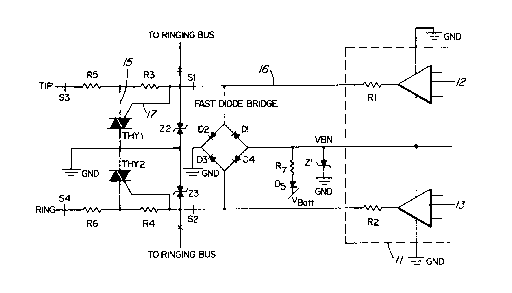
The second preferred embodiment of the protection
circuit of the invention is illustrated by Figures 6 and 7.
Figure 6 is a circuit diagram, and Figure 7 is a schematic
representation of four current versus time profiles obtained at
selected points on the circuit of Figure 6. The second embodiment
differs from the first embodiment by the inclusion of a diode
bridge consisting of four standard low voltage diodes D6, D7, D8
and D9, and two additional resistors R8 and R9. The diodes D6 to
D9 each have a sufficiently high reverse breakdown voltage to
support the maximum battery voltage of -48 volts. They also have
a typical forward recovery time in the order of one microsecond.
One type of diode suitable for this purpose is the lN4001 type.
Assuming the presence of a negative voltage surge on the
TIP line of Figure 6, the second embodiment operates in the
following way. The voltage is clamped initially by diode Dl at
the output 20 of the SLIC circuit to approximately one diode drop
below battery voltage, ie. -48.6 volts. As the current passing
through diode Dl increases, voltage differentials grow across each
of the resistors R5, R3 and R8. The voltage differential across
resistor R8 forces diode D5 into conduction. The response time of
diode D6 is considerably slower than the four nanoseconds of diode
Dl, but is sufficiently fast that relief is provided to diode Dl
before high current flow can damage it. Diode D6 in turn requires
relief from high current flow if it is to avoid damage, and triac
--10--
THYl provides that relief. The presence of diode D6 allows the
use of a more slowly responding, and thus cheaper, triac than was
used in the first embodiment; the response time of triac THYl in
the second embodiment may be as high as several microseconds. As
in the first embodiment, triac THYl is turned on by the voltage
differential created across the resistor R3. A positive voltage
on the TIP input causes a corresponding action. In that case,
diode D2 initially clamps the positive voltage to ground voltage,
then current flow through resistor R8 causes diode D7 to begin
conduction, and then triac THYl is triggered by current flow
through resistor R3. The protection circuit comprises a
corresponding set of components for handling negative or positive
voltage surges on the RING input.
The presence of capacitor Cl improves the fast surge
performance of the triac. Cl is the type of capacitor usually
employed for decoupling, having a value in the order of 0.1
microfarads; it provides a virtual ground for fast pulses. The
arrangement will ensure that triac THYl will turn on for voltage
ramps above a certain value, due to the generated current
(C)(dV/dt).
In the embodiments of Figures 3, 4 and 6, a pair of
bipolar zener diodes Z2 and Z3 are shown. Z2 is positioned
between the TIP line and ground, and Z3 is positioned between the
RING line and ground. Z2 or Z3 turns on whenever the voltage
differential across it exceeds approximately 250 volts, ie.
whenever the TIP line or RING line exceeds +250 volts or -250
volts. Solid-state relays Sl and S2 can alternately connect
either the SLIC or the telephone ringing circuitry to the TIP and
RING lines. The purpose of Z2 and Z3 is to protect the
solid-state relays. When a voltage surge occurs on the TIP or
RING line, Z2 or Z3 respectively momentarily clamps the voltage to
less than 250 volts until triac THYl or triac THY2 respectively
can turn on to shunt the surge to ground. Z2 and Z3 thus serve a
similar protective function for the solid-state relays as that
served by the diode bridge(s) for the SLIC.
Once a surge on the TIP or RING lines has been shunted,
the triac THYl or THY2 can be reset in one of several ways. The
SLIC can be programmed to sense when the drivers are saturated
~ 1 '7) ~ 7 ~
during the shunting of the triacs, and to momentarily open the
relays Sl and S2 to remove current from the line to reset the
triacs. Alternately, the triacs THYl and THY2 can be designed
with a high holding current; such triacs will automatically turn
off when the fault current drops below the holding current of the
triac. The triac will also turn off after the surge and the
ringing current drops below the holding current. This will occur
during the zero crossing of the rihging current.
The protection circuits that have been described may be
integrated into monolithic silicon devices.