Note: Descriptions are shown in the official language in which they were submitted.
I :) r) 7 `) ~ 1
8IG~ VO~AGE ~LECT~P~ORESlS A~ARATU~
Background of the Tnvention
This invention relates to electrophoresis equipment and,
more particularly, to a method of applying alternating high
voltage fields across an electrophoresis medium.
Electrophoretic methods make use of the difference in
mobility between charged particles, suspended in a supporting
medium and subject to the influence of an electrical field,
to separate such particles from one another. The mobility of
a charged particle is principally influenced by its charge-
to-mass ratio but may be affected by a number of other
factors including, importantly, the interference between the
migrating particles and the structure of the supporting
medium. Particles of similar charge-to-mass ratio may
therefore be separated by exploiting the difference in their
physical interaction with the support medium, which in turn
1~ is chiefly the result of differences in the migrating
particles' size and shape.
If the electrical field to which the migrating particles
are subjected may be varied, particles with similar charge-
to-mass ratio may be separated by yet another means which
takes advantage of differences between the particles relative
ability to reorient themselves under a fluctuating electrical
field.
Carle, et al., International Patent No. PCT/~S 86~02038,
discusses the separation of D~A molecules with similar
charge-to-mass ratio through the use of pulsed or reversing
electrical fields along one axis of the supporting medium.
Carle, et al., postulate that such mollcùles, under a uniform
field, orient themselves with respect to their migration, so
as to have approximately equal mobility despite differences
in their length. In an alternating field, however, the
longer molecules are unable to adjust their orientation to
the changing field as rapidly as the shorter molecules and
hence cannot maintain a high mobil~ty orientation.
Separation of such molecules is obtained b~ alternating the
electrical field across the supporting medium at the
appropriate frequency to accentuate the difference in
mobility between the longer and shorter molecules. The time
period of one of the two polarities of voltage is adjusted to
be longer than that of the reversed polarity insuring a net
migration of molecules in one direction. An analogous
procedure makes use of switched fields of different voltage
rather than different periods.
Carle, et al., also disclose a means of using a pulsed
rather than polarity switche~ electric field to separate
certain molecules. Under this approach, the molecular
separation results from an intrinsic propensity of the
molecule to "relax" into lower mobility configurations in the
absence of an applied field. The ability to separate
molecules under this approach results from differences in
"relaxation" time and reorientation from "relaxatlon" time
between such molecules.
A different technique using alternating electrical
fields across a supporting medium is disclosed in Cantor &
Schwartz, U.S. Patent No. 4,473,452 which discusses the
application of two transverse alternating electrical fields
along a ?lane of supporting medium. Such transverse fields
may be of different voltages and m~ a-r~ed in their angle
to each oth~r and may be pulsed or reversed in polarity.
The practical implementation of all of the above-
described modulated field techniques requires one or more
power sources that may be switched on and off or reversed in
polarity automatically to provide a periodic variation in
field intensity across the supporting medium. At the present
time, these techniques involve total field voltages of less
than several hundred volts and such power sources are
constructed of a combination of a DC power supply of correct
voltage and current rating in combination with a mechanical
or solid state relay of a type commercially available. The
relay is then actuated by a lower voltage timing module.
As modulated field electrophoresis techniques are
developed, it is believed that voltages of several thousand
volts or more will be required in order to realize two
benefits. The first benefit of using such high voltages in
these techniques is that for a given field gradient
(expressed in volts per length of support medium) a higher
voltage allows larger separation area which in turn may
result in greater separation distances between migrating
particles and hence improved resolutionO The second benefit
of higher electric fields is that the speed of migration of
charged particles is approximately proportional to the
strength of the gradient and therefore at high voltages the
the separation process may be greatly accelerated.
Nevertheless, there are significant obstacles to the use
of high voltages, the most significant being the difficulty
of reliably switching high DC voltages over many cycles. The
prior art has made use of mechanical relays and has suggested
the use of so called "solid state" relays.
1 )f~17)~1
The use of mechanical relays is severely limited in
higher voltage applications as a result of increased
propensity of higher voltage to arc across relay contacts
during each relay cycle. Over many repetitions this arcing
pits the relay contacts ultimately causing their failure.
The expected lifetime of a mechanical reed relay operated at
high voltages and switched once every several seconds may be
less than one month. Some field modulated electrophoretic
techniques require switching times as fast as once every
several milliseconds.
Solid state relays solve the contact wear problem but
are generally available only for relatively low voltages.
Such solid state relays are typically composed of triggering
circuitry, possibly including an optical isolator to allow a
"floating voltage" trigger signal, and a solid state switch
element, frequently a MOSFET. It should be noted that the
commonly available and somewhat higher voltage Triac or SCR
based solid state relays are intended for switching
alternating currents and require the switched voltage to drop
to zero before they will reset. These switches cannot be
used in a electrophoresis design where DC voltages must be
switched.
Commercially available solid state relays generally
cannot be combined or "stacked" to handle higher voltages
because of limitations of the driving circuitry. More
precisely, the triggering circuitry on most D.C. solid-state
relays is voltage referenced to one side of the switch so
that if the switches are placed in series, the relay
triggering voltage can no longer be precisely determined.
3C Further, because of the tendency of such devices to switch
asynchronously, an individual device in a stacked
) n ~
configuration may be subjected to many times its maximum
rated voltage.
Solid state relays with "isolated" trigger circuitry may
overcome this first obstacle to stacking, that imposed by the
referencing of the trigger circuitry to the switch itself,
but generally suffer from high trigger circuit impedances.
Optically coupled devices are limited by the relatively high
impedances of optically sensitive circuitry. Circuits
triggered by capacitively or inductively isolated D.C.
pulses, where the pulses toggle the relay on and off, are
also high impedance circuits as a necessary result of the low
energy transferred by a single pulse at practical voltage
levels. Further, these pulse triggered circuits are
necessarily sensitive to pulse-like capacitively coupled
noise. The switching of high voltage fields across a
supporting medium, in high voltage modulated field
electrophoresis, by definition, involves the rapid switching
of high voltages. This switching produces capacitively
coupled high amplitude voltage spikes which makes
susceptibility to electrical noise particularly acute in
these applications. The polarized nature of most solid state
switching devices and the need for reversing the polarity of
the applied field in modulated field electrophoresis
techniques requires that a number of solid state switches be
connected to each other. This in turn, increases the
possibility that any voltage spikes developed by one switch
will be capacitively coupled into the switching trigger
circuitry of another switch.
7 ~
Finally, conventional solid state relays are generally
designed to provide the maximum attainable speed of switching
transition between the "on" state and the "off" state. This
is to reduce the power dissipated in the solid state
S switching element and thereby increase the average current
that may be handled by the device. Unfortunately, such rapid
switching speeds increase the amplitude of voltage spikes and
thereby increase the chance of false triggering of other
switches in an electropnoresis application, and the chance of
interference with other sensitive laboratory equipment.
` !! 7 ~
maLy of th~ Tnventi~
The present invention relates to a means of reliably
switching high voltages for use in modulated field
S electrophoresis processes. The invention can be used with a
microprocessor controlled timing means connected through
controlling circuitry to a number of high voltage solid state
switches which may selectively connect an external high
voltage DC power source across one of several pairs of
electrodes.
One advantageous feature of the invention, therefore, is
~hat it provides a reliable means of switching high voltage
DC power, in modulated field electrophoresis applications,
without the problems of contact failure or mechanical
actuator failure attendant to mechanical relays.
~ :7n;~ ?l
The herein described controlling circuitry for the solid
state switches produces an AC signal during the entire time
that the solid state switch is turned on. This AC signal is
rectified and filtered to produce a high current capacity DC
triggering voltage which is continuously applied to the gate
of the solid state switching device during the device's "on"
period. The high current capacity of this continuous DC
triggering voltage helps the solid state switch resist being
turned off by external, negative voltage spikes. When the DC
triggering voltage is not present, a discharge circuit
provides a low impedance path to ground from the gate of the
solid state switching device to prevent the solid state
device from being turned on by positive, external voltage
spikes. Such voltage spikes of both polarities are common in
modulated field electrophoresis applications where high
voltages are commutated by a plurality of switches in close
proximity to each other.
Accordingly, another advantageous feature of the
invention is that it provides a trigger means for a solid
state switch that is resistant to positive and negative high
voltage noise spikes resulting from the switch action of
adjacent switches in electrophoresis applications.
l ~ n 7 ~
In order to achieve higher voltages with available, less
expensive, lower voltage solid state devices, the devices may
be connected in series. In such a configuration, the trigger
voltages for e~ach solid state device must be floating, that
is, without reference to any voltage outside of the trigger
circuitry. The reason for this is that the absolute trigger
voltages for each solid state device in series is unknown
during the time the device is switching except with respect
to the solid state switching device itself. The continuous
AC trigger signal provides a means of coupling the trigger
through a transformer so that the rectified and filtered DC
trigger voltage will be floating. Further, as an added
benefit, because the resulting DC trigger voltage has high
current capacity, it may serve as a floating power supply for
the remainder of the trigger circuitry thus avoiding the need
for an additional floating power supply
It is therefore another advantageous feature of the
invention that lt provides a means for combining lower
voltage, high gain, solid state switching elements to produce
a higher voltage switch from readily available lower cost
components.
Still further, in the present invention, a series
resistor is placed between the DC trigger voltage and the
gate of the solid state switching device to slow down the
speed of the switching action and, by reducing the rate of
change in voltage across the device, thereby reduce the
electrical noise produced by the switch itself. A resistor
may be used because the DC trigger signal is not a pulse but
is a continuously applied DC voltage. Unlike a DC pulse
controlled system, in the present invention there is no
danger that such a series resistor will sufficiently reduce
' ,) () ;~ ~ ,' 1
the energy from the trigger signal so that the switch is
unable to turn on.
It is therefore yet another advantageous feature of the
invention that it provides a means for switching high
voltage, in modulated field electrophoresis techniques, so
that the switching speed is limited to reduce the amplitude
of generated capacitively coupled voltage spi~es that may
interfere with other switch triggers or external electronic
instrumentation.
The foregoing and other advantages of the invention will
appear from the following description. In the description,
reference is made to the accompanied drawings which form a
part hereof, and in which there is shown by way of
illustration a preferred embodiment of the invention. Such
embodiment does not necessarily represent the full scope of
the invention, however, and reference must be made to the
claims herein for interpreting the breadth of the invention.
~ief DescriptiQn of th~-~raw mg~
Figure 1 is a simplified block diagram of a modulated
field electrophoresis device showing a cell for experiments
involving transverse fields.
Figure 2 is a schematic representation of an alternate
cell configuration for field inversion electrophoretic
experiments.
Figure 3 is a detailed schematic of the switch control
logic.
Figure 4 is a detailed schematic of a representative
solid state switch, SW1.
f ~' ? 1
a~s~ tiQn Qf ~h~ Preferred ~mhod;~en~
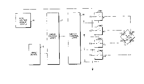
Figure l illustrates, in schematic, a field modulated
electrophoresis device incorporating the present invention.
A high voltage power supply 15 producing, e.g., 3000 volts DC
and several hundred milliamps of current, is connected to one
side of two solid state switching elements SW1, and SW2 at
points T1 and T2. A generalized electrophoretic cell is
shown as l9. Four electrodes 20-23 are shown positioned
about the periphery of the cell at 30 increments. The
construction of such cells may vary depending on the
experiment to be performed as is generally described in
prior art, such as, Carle et al. U.S. Patent No. 4,737,251
and the references cited therein. Electrodes 20 and 23 are
connected to point P1 and P2 of respective switches SW1 and
SW2 so that each such electrode may be raised to the voltage
of the power supply 15 when the respective switch is
activated.
In a similar manner, solid state switching elements S~3
and SW4 serve to connect electrodes 21 and 22 to ground when
the given switch is actuated. Proper sequencing of switching
elements SW1-4 allows alternating electric fields to be
established in the plane of the cell as shown by arrows 24
and 25.
Referring to Figure 2 there is shown an alternate cell
design used for field inversion electrophorectic techniques.
In this cell design, electrodes 20 and 22 have been
electrically joined into a single electrode as have been
electrodes 21 and 23. The alternate activation of solid
state switches SW1 and SW3, together, and switches SW2 and
1 3 n ~
SW4, together, produces alternating, opposing electric fields
24 and 25 as shown in Figure 2.
As will be described in more detail below, switch
control logic 18 serves to actuate the switches SW1-SW4.
This control logic is driven by the timing control logic 17,
which may consist of a commercially available sequence timer
or programmable controller capable of producing logic level
signals. An input device 16 permits reprogramming of the
timing control logic 17 by the user.
Referring now to Figure 3, there is shown a detailed
schematic of the switch control logic 18 as shown in Figure
1. Input signals E and F are logic level signals received
from the timing control logic 17. When signal E is a logic
'l', SW1 and SW3, shown in Figure 1, are closed. When signal
F is a logic '1', SW2 and SW4, also shown in Figure 1 are
closed. Signals E and F and may be activated in any
sequence determined by the experimenter subject to the
constraint that both E and F may not be simultaneously in the
logic "1" state. The circuitry driven by signal F is
identical to the clrcuitry driven by signal E, and although
the circuitry for signal E will be described it should be
understood that the same description applies to the circuitry
for signal F.
Resistor R1 in combination with D1, Cl and Schmitt
trigger NAND Gate 1 form a pulse delay circuit which ensures
that during the simultaneous transition of signal E to a
logic '1' state and signal signal F to a logic "o~ state, or
vice versa, the outputs of both gate 1 and gate 2 are in a
logic '1' state prior to either gate dropping to a logic '0'
state. The purpose o~ this is to ensure that there is no
period during which all four switches SW1-4 maybe closed
1:7)f~ 7 ) 2 1
thereby short circuiting the high voltage power supply 15.
When the signal at point E is in a logical "0" state, current
is conducted through Dl ~ischarging capacitor Cl. NAND Gate
1 turns off at its switching threshold, which for a CMOS
Schmitt trigger is approximately one-third of th~ power
supply voltage. When the signal at point E rises to logical
"1", diode Dl is reverse biased and therefore does not
conduct and capacitor Cl must charge through resistor R1 to
approximately two-thirds of the power supply voltage before
gate 1 can turn on. The speed of this charging process and
hence the delay in the switching of gate 1 may be adjusted by
altering the RC time constant which, in this case, is
approximately 10 microseconds.
Accordingly, a logic "1" signal at point E produces a
logic "0" signal at the output of NAND Gate 1 which when
applied to diode D3, reverse biases D3, effectively
disconnecting the output of Gate 1 from inverter Gates 3 and
4 and their associated circuitry. Inverter gates 3 and 4 are
logic inverters configured as an oscillator circuit such as
that described in RCA publication ICAN-5267 "Astable and
Monostable Oscillators Using RCA COS/Mos Digital Integrated
Circuits". When the applied signal is low, this oscillator
is activated and produces a 2.5 to 3 megahertz square wave,
bounded by the logic state voltages, at the output of
inverter gate 4
This high frequency square wave is applied to the inputs
of inverter gates 7-10 which are connected in parallel so as
to provide increased current sourcing and sinking capacity to
drive transistors Q1-Q4. Transistor pair Q1 and Q2 and
transistor pair Q3 and Q4 are configured as "push-pull"
amplifiers to provide further increased current sourcing and
5 ~1 .1 ~ ,'~ I
sinking capability on the order of several hundred
milliamperes. Capacitors C9 and C10 form part of a resonant
circuit in connection with the transformer coil primaries
TR1-4 to which they connect as will be described further
below. Transistor pairs Ql and Q2 and transistor pair Q3 and
Q4 are switched by the same signal but each pair is connected
to a different switch SW1 through SW4.
Referring now to Figure 4 there is shown a detailed
schematic of solid state switching element SW1. .Switching
elements SW2-4 are identical in construction with SW1, and
therefore, only SW1 will be described. SW1 is composed of
four stages each of which is identical and all four of which
are connected in series as shown in Figure 4. Accordingly,
only stage 1 will be discussed in detail. The high frequency
A.C. signal from transistor pairs Q1 and Q2 of Figure 3 is
connected to stage 1 of switch SW1 at the primary winding of
a toroid transformer TR1. The current flowing through the
primary of TR1 then flows through the primary of TR2 of stage
2 and TR3 of stage 3 and TR4 of stage 4 before flowing to
ground, thereby serving to trigger each of the four stages of
switch element SW1 at the same time and in a similar manner.
Referring again to the detailed schematic of stage l, the
signal to the primary side of toroid transformer TR1 induces
a voltage on TRl's secondary side according to a primary to
secondary turns ratio of 1:10. The resulting high frequency
signal is applied to D5 and C13 which form a half wave
rectifier producing a DC voltage at the ~unction of D5 and
C13. This DC voltage forward biases D6 and current flows
through resistor R8 to bias MOSFET M1 into conduction. R8
acting in conjunction with Ml's effective capacitance serves
to limit the speed with which M1 turns on, and therefore
14
1 - n./, ~ I
serves to reduce radio frequency noise generated by the turn-
on of Ml. Transistor Q9 is effectively reversed biased
because its gate voltage during the turn-on of M1 is at all
times higher than or equal to the voltage at its emitter.
During the time when Ml is turned on, a high current
capacity, low impedance D.C. voltage source is constantly
applied to its gate, minimizing the possibility of accidental
turn off resulting from coupled noise signals. When the
signal at A is turned off the voltage at the junction of D5
and C13 begins to drop, the charge on C13 being conducted
through R7. When the voltage at the junction of C13 and R7
drops to approximately seven-tenths of a volt less than the
voltage at the junction of R8 and the gate of M1, Q9 is
biased into conduction, rapidly discharging any remaining
voltage at the gate of M1. Accordingly, M1 is biased off
more rapidly than would be the case if its bias voltage were
to drop slowly with the decay of the voltage at the junction
of C13 and R7~ In the off state, the gate of M1 is connected
to ground through a low impedance path through Q9 of
approximately 100 ohms equivalent resistance.
Zener diode Z1 serves further to protect M1 from
capacitively induced voltage spikes resulting from switching
of the other switches in the electrophoresis device. Zener
diodes Z2-Z5, which each have a breakdown voltage of 200
volts, serve to protect Ml which has a breakdown voltage of
800 volts from potentially damaging voltage in the event that
the stages of SW1 swi~ch at slightly different times. When
SWl is off there is no current flowing through line T1.
Accordingly, the voltage is equally divided across M1, M2, M3
and M4. When switch 1 is fully turned on the resistance of
~1, M2, M3 and M4 is very low and accordingly the total
.
I :7, n ,~
voltage across each switch is on the order of a few tenths of
volts to one volt depending on the particular device
characteristics and the resistance of the electrophoresis
cell. A potential problem arises during the actual switching
if one stage switches substantially after the others. If
solid state devices M2, M3 and M4 switch prior to M1, M1
would see a full 3000 volts across its terminals absent its
protection from diode Z2-5. The presence of diodes Z2-5
ensure that the voltage across terminals of stage 1 will
never exceed 800 volts. Voltages above 800 volts will cause
diodes 2-5 to conduct for the short period of time necessary
for stage 1 to catch up with the other stages. Accordingly,
the use of diodes Z2-~ enable the various stages to be placed
in series as shown without asynchronous switching between the
stages destroying an individual stage MOSFET.
In an alternative embodiment, not shown, additional
stages may be added to each switch SW1-4 in order to permit
the switching of higher voltages for use in applications such
as capillary electrophoresis. The limit to such additional
stages is determined primarily by the ability of the switch
control logic 18 to drive additional transformer primaries,
e.g., in series with TRl-4.
16