Note: Descriptions are shown in the official language in which they were submitted.
ANTI-FRAUD DEVICE EOR USE WITH
A COIN OPERATED TELEPHONE INSTRUMENT
BACKGROUND OF THE INVENTION
1 The present invention relates generally to coin
operated telephones and deals more specifically with
apparatus for preventing fraudulent calling initiated with
a "tip-to-ground" fraud condition to defeat detection of a
coin collect supervisory signal at the telephone
instrument.
Coin operated telephone instruments are well
known and understood in the art and the problem of
fraudulent calling due to the generation of coin deposit
audio slgnals to simulate coin deposit into the telephone
instrument is also well recognized. Accordingly, there
are numerous devices and proposed solutions for preventing
acoustically oriented fraudulent calling and include, in
some instances, complex circuit arrangements in the
telephone instrument and in the various telephone offices
serving the telephone instrument. However, none of the
known prior devices recognize or prevent fraudulent
calling due to "tip-to-ground" fraud conditions which is
commonly referred to the telephone industry as "pin
fraud". It is estimated that revenues lost in the United
States alone due to l'pin fraud" may approach millions of
dollars annually.
F ~ , ~
1 "Pin fraud" describes a type of fraudulent
calling where a pin or other small metallic object is
inserted into the transducer or transmitter element in the
mouthpiece of the handset and which pin is used as a
contact to electrically short circuit the telephone
subscriber line to ground potential to prevent the coin
collect supervisory electrical signal from operating the
coin collect circuitry within the telephone instrument,
thereby, causing coins temporarily held in a coin hopper
to be returned to the telephone user rather than the coin
collection box within the telephone instrument. It is
also possible to commit "pin fraud" by inserting the pin
into the transducer or receiving element in the earpiece
of the handset to provide the contact for short circuiting
the telephone line to ground potential. Although the
transmit~er and receiver elements are generally used as
the access points for initiating a "tip-to-ground" fraud
condition, the fraud condition may also be introduced
through the cord connecting the handset to the telephone
instrument.
Therefore, it is an object of the present
invention to provide an anti-fraud device for use with a
coin operated telephone instrument which prevents
fraudulent calling due to "pin fraud".
It is a further object of the present invention
to provide apparatus for preventing fraudulent calling due
1' ~ ` ~ ,/ i
1 to "tip-to-ground" fraud conditions which prevent the
collection of deposited coins.
It is a yet further object of the present
invention to provide an anti-fraud device which is located
internally in the telephone instru~ent housing and without
the requirement of additional special circuitry in the
telephone office æerving the telephone instru~ent.
1 SUMMARY OF THE INVENTION
In accordance with the present invention, an
anti- fraud device for use with a coin operated telephone
instrument to prevent fraudulent calling due to "pi.n
fraud" is presented. The device is connected to the
transmission network located in the telephone instrument
in which the network connects the telephone instrument to
the telephone subscriber line to send and receive
electrical signals representative of audio and call
supervision to and from the telephone line. The
transmitter element of the telephone instrument is
arranged in series with contacts of a dual coil, dual
contact latching relay to electrically connect and
disconnect the transmitter element to and from the
transmission network and accordingly, the telephone
subscriber line. An "ON-HOOK/OFF-HQOK" sensor detects the
- presence of an "OFF-HOOK condition at the telephone
instrument and activates a timer which produces voltage
signals a~ pre-determined tlmed intervals in response to
the sensing of an "OFF-HOOK" condition. A ground sensing
circuit is connected to the transmitter element through a
contact of the relay and provides a voltage signal
representative of a ground fault condition in response to
the presence of an electrical ground poten~ial at the
transmitter element. ~he touch-tone dial keypad of the
telephone instrument is coupled to the anti-fraud device
and activations associated with the keypad are sensed and
~ ~ r~-;7 ~ -,T,
1 are inputted to a counting circuit which counts the number
keypad activations after the sensing of an "OFF-HOOK"
condition. The counter produces an output voltage pulse
after counting a pre-determined number of activations and
which output voltage is used to reset the relay to
disconnect the transmitter element from the telephone
transmission network and the telephone subscriber line.
After the pre-determined number of keypad activations are
counted the transmitter element is disconnected until such
time as the anti-fraud device is reset when the telephone
instrument is returned to an "ON-~OOK" condition. This
feature prevents defeat of the anti-fraud device through
repeated keypad activations which would otherwise deplete
the energy stored in a capacitor of the power supply which
is used to power the electric components of the circuit.
A second counting circuit is coupled to a ground sensing
circuit and counts the number of occurrences of the
presence of an electrical ground potential at a terminal
of the telephone transmission network. There are
occassional ground conditions present at the network
during the course of a telephone connection due to the
operation of a telephone switching network. The counter
is arranged to count a pre-determined number of ground
occurrences during a pre-determined time interval set by a
timing pulse generator. The ground occurrence counter is
reset to a zero count at the beginning of each reset
interval to accommodate the occassional normally expected
1 ground occurrences. Upon counting the pre-determined
number of ground occurrences during the pre-determined
interval, an output signal from the counter is used to
cause the operation of the relay to reset it to disconnect
the transmitter element from the telephone transmission
network and the subscriber line. Consequently, the
presence of a ground fraud condition at the transmitter
element causes the relay to reset to disconnect the
transmitter element which permits the coin collect
supervisory signal sent from the telephone office serving
the telephone instrument to activate the coin collect
relay within the telephone instrument in the presence of a
ground at the transmitter element which causes the
deposited coins to be transferred to the coln collection
box within the telephone instrument.
The invention further includes isolation means
for electrically coupling the receiving element of the
handset to the telephone instrument transm$ssion network
whereby a "tip-to-ground" fraud condition is prevented
from being introduced at the receiving element and the
telephone cord coupling the handset to the telephone
instrument.
I BRIEF DESCRIPTION OF THE DRAWINGS
Additional features and advantages of the
present invention will become readily apparent from the
following description and the drawings wherein:
Fig. 1 is a perspective view of a coin operated
telephone instrument with which the anti-fraud device of
the present invention may be used. The telephone housing
is shown partially cu~ away to reveal a circuit board
containing the electronic components comprising the anti-
fraud device.
Fig. 2 is an exploded view of a typical handset
used with the telephone instrument showing a pin inserted
through the mouthpiece cover into the transmitter element.
The pin is connected to a ground reference voltage
potential to defeat telephone coin collection circuits and
permit fraudulent calling.
l Fig. 3 is an electrical circuit schematic
diagram illus~rating one embodiment of the anti-fraud
device of the present invention.
DETAILED DESCRIPTION OF PREFE~RED EMBODIMENTS
Referring to the drawings and considering Fig~ 1
in particular, a coin operated telephone instrument of the
general type with which the anti-fraud device of the
present invention may be used is shown therein and
designated 10. The telephone 10 includes a housin~ 12
generally of metal construction, a conventional handset 14
connected to the telephone instrument and a transmission
and balancing network within the telephone
instrument by a cord 16. The transmission network may be
one of a number of different types and is generally well
understood by those who are skilled in the telephone
transmission part. The telephone 10 further includes a
coin slot 18, a coin release 20, a touch-dialing keypad
shown generally at 22 and located on the face 24 of the
telephone instrument 10 and a coin return chute 26 also
located on the face of the telephone instrument. A
por~ion of the telephone housing 12 is cut away to reveal
a terminal connection block 28 which is used as a
connection point for the various components comprising the
telephone instrument. A circuit board or module 30
containing the electrical components comprising the anti-
l fraud device of ~he present invention is connected to the
terminal block 28 by leads 32, 32.
The telephone instrument 10 is also connected to
the telephone subscriber line in a conventional manner to
send and receive electrical signals representative of
audio, speech and call supervision. The audio or speech
is generally converted by a carbon microphone or a
transmitting element in the mouthpiece of the handset to
electrical signals which are coupled to the telephone
subscriber line. Received electrical signals are
i converted into audio by a transducer generally located in
i the
earpiece of the handset. The operation of the
! transmitting element and receiving transducer are
generally well known in the art and a further
understanding of their operation is not essential to the
disclosure of the anti-fraud device of the present
invention.
Referring now to Fig. 2 an exploded view of a
typical handset 14 is shown therein illustrating the
carbon microphone or transmitting element 34, a receiving
cup 36 having contacts 44 and 46 for making electrical
connection with the transmitting element 34 in a well
known manner. The transmitting element 34 and receiving
cup 36 are held within the handset by the mouthpiece cover
38. The mouthpiece cover 38 includes a number of openings
40, 40 which permit the acoustic excitation of the
l transmitting element 34. The handset 14 is also shown
having a receiving element 35 which is held within the
handset by an earpiece cover 37. The earpiece cover 37
includes a number of openings 39, 39 which permit acoustic
signals produced by the receiving element to be
transmitted to the telephone user.
As illustrated in Fig. 2, a fraudulent grounding
condition is introduced via a pin or similar metallic
object 42 inserted through one of the openings 40 in the
mouthpiece cover 38 and into contact with the transducer
element 34. The telephone user then has access via an
external grounding lead attached to the pin 42 to
introduce an electrical ground potential at an appropriate
time during the telephone call to defeat the coin
collection supervisory signal which is applied in a manner
known to those skilled in the art to the coin collection
circuitry within the telephone instrument. As shown in
the figure, the transmit element 34 is electrically
connected to the telephone instrument via the cord 16
which includes a pair of wires 48 which terminate at the
contacts 44, 46.
The fraudulent grounding condition may also be
introduced via a pin inserted through one of the openings
39 in the earpiece cover 37 and into contact with the
receiving element 35 which is electrically connected to
the telephone instrument transmission network via a pair
of wires 49 in the cord 16. Alternately, the cord 16 may
1 be pierced to introduce the fraudulent groundiny
condition.
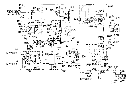
Turning now to Fig. 3, an electrical circuit
schematic diagram showing the major electrical components
comprising one embodimen~ of the anti-fraud device of the
present invention is shown therein. It will be understood
that the specific circuit designs may vary as a direct
result of the designer's choice of electrical components
and type. Preferably, the anti-fraud device of the
present invention is implemented using electrical
components having a low power consumption requirement such
as, for example, devices designed and fabricated using
CMOS technology to minimize power consumption and current
drawn ~rom the telephone subscriber line.
The anti-fraud device of Fig. 3 is coupled to
the tip and ring of a telephone subscriber line through
the telephone instrument's transmission network input
leads 52, 54 which also couple a power supply of the
device represented by the dashed line box 50. When the
telephone instrument is in an "ON-HOOK" condition, current
is provided through the input leads 52, 54 which are
connected to a standard diode bridge 56. The bridge 56
comprises diodes 58, 60, 62 and 64 arranged in a full wave
bridge configuration. Lead 52 is connected to the
junction formed by the cathodes of diodes 62 and 64 and
lead 54 is connected to the junction formed by the anodes
of diodes 58 and 60. The junction formed by the anode of
1 diode 62 and the cathode of diode 60 is connected to a
common reference or ground potential designated 66. A
capacitor 68 is charged primarily during the time that the
telephone instrument is "ON-HOOK" due to current flowing,
for example, through lead 52, diode 64, diode 70 and the
series resistor 72 through the capacitor 68 to the ground
reference potential continuing through the diode 60 and
finally to the other side of the telephone line at
terminal 54. During instances of battery reversals, such
as, for example when going "ON-HOOK" and during
supervisory signalling, the bridge 56 again charges the
capacitor 68 to the voltage potential developed across the
bridge between the points defined by the junction of the
cathode of diode 60 and anode of 62 and the junction
defined by the cathode of diode 58 and the anode of the
diode 64. When the telephone instrument is in an OFF-
HOOK" condition, a very low impedance appears across
terminals 52 and 54 which effectively places a negative
voltage potential at the inputs to the bridge circuit 56.
Diode 70 blocks the current flow and accordingly, stops
charging the capacitor 68. The capacitor 68 now
discharges through zener diode 74 and a voltage designated
"+ VOLTAGE" is developed at the junction of the cathode of
zener diode 74, one end of capacitor 68 and one end of
resistor 72. The "+ VOLTAGE" is used to power the
electronic componen~s of the apparatus of the present
invention.
' ~`1 ' ' ' '
13
l An "ON-HOOK" - "OFF-HOOK" sensing ~ircuit
designated by the dashed line box 76 has an input 78
connected to the junction of the cathode of diode 58 and
the anode of diode 64 of the bridge 56 and an "OFF-HOOK"
condition presents a negative voltage potential which
forward biases zener diode ~0, the diode 80 having its
anode connected to the series resistor 82 between it and
the input 84 of a Schmitt trigger circuit 86. A resistor
88, zener diode 90 and the capacitor 92 shunt the input 84
lO to ground reference potential 66 to dissipate spike
voltage transients and filter any noise which may be
present at the input 8~. The output 94 of the inverter 86
is fed to the input of a second inverter 96 whose output
98 is fed to an OR logic circuit designated by the dashed
line box 100. The output 98 forms one input to an OR
logic gate 102 within the logic circuit 100. In the "ON-
HOOK" condition, the output 98 is at a logical high
voltage level and when the telephone instrument is in an
"OFF-HOOK" condition the output 98 is at a logic low
voltage level.
The touch-tone dial keypad is coupled to the
anti-fraud device via terminal 104 and it serves as the
input to a sensing circuit indicated by the dashed line
box 106 which circuit senses each activation of a button
on the touch-tone dial keypad. Signals from the keypad
appearing at the terminal 104 are coupled to an input 108
of an opto-isolator 110. A signal appearing at the input
14
l 108 causes the opto-isolator 110 to produce a voltage
signal at its output 112 causing the voltage level at the
output 112 to drop from the "+ VOLTAGE" potential present
at one end of the resistor 114 and which is coupled to the
output 112 to the ground reference potential during the
activation of the keypad. This voltage signal transition
is coupled to the input 116 of an inverter 118,
configured as a Schmitt trigger, which causes its output
120 to change state from a ground reference potential to a
logical high voltage potentialO The output 120 serves as
the input to a counting circuit designated by the dashed
line box 122 and forms an input to the logic OR gate 102.
The counting circuit 122 includes a binary
ripple counter 124 which is configured to produce a
logical high voltage signal at its output 126 upon
achieving a predetermined count of button activations at
the touch-tone dia] keypad. The output 126 of the counter
124 forms another input to the logic OR gate 102. The
counter 124 also includes a reset input 130 which resets
the counter to zero upon a change in state of the
telephone instrument from an "OFF-HOOK" condition to an
"ON-HOOK" condition. The purpose of the counter is to
prevent the telephone user from depleting the power supply
voltage capacity provided by the charge on the capacitor
68 as explained above, and thus defeating the anti-fraud
device through removal of power.
l The anti-fraud device also includes a ground
sensing circuit designated generally within the dashed
line box 132 and has an input 134. The ground sensing
circuit 132 includes a full wave bridge 136 comprising
diodes 138, 140, 142 and 144 configured in a full wave
bridge arrangement. The input 134 is connected to the
junction formed by the anode of diode 134 and the cathode
of dlode 138. The opposite side of the bridge formed by
the junction of the anode of diode 142 and the cathode of
diode 140 is connected to the electrical chassis ground
potential indicated by the symbol 146. The bridge 136 is
further coupled to the input terminals 148, 150 of an
opto-isolator circuit 152 with the input 148 being
connected through a resistor 154 to the junction formed by
the cathodes of diodes 142 and 1~4. The input 150 is
connected to the junction formed by the anodes of diodes
138 and 140. When a voltage signal is present at the
input 134, the bridge 136 provides a path through diode
144, through the resistor 154 to the input 148 thereby
forward biasing the light emitting diode of the opto-
coupler by completing the circuit path through the input
150, through the forward biased diode 140 to the chassis
ground 146. The presence of a voltage at the input 134
causes the output 156 of the opto-isolator 152 to be at a
ground reference potential. The output 156 of the opto-
isolator 152 is connected to the input 158 of an inverter
160 configured as a Schmitt trigger. The output 162 of
I ~ n77`~
l the inverter 160 is at a logical high voltage potential
when a voltage is present on the input 134 of the ground
sensing circuit 132. The output 162 is coupled to the
input of an inverter 164 configured as a Schmitt trigger
and its output 166 forms another input to the OR logic
gate 102 and is at a ground reference voltage potential
when a voltage signal is present on the lnput. 134.
The output 162 of the inverter 160 is also
coupled to the input 168 of a ground occurrence counting
circuit designated by the dashed line box 170. The ground
occurrence circuit 170 includes a binary ripple counter
172 arranged to count a pre-determined number of ground
occurrences present at its input during a pre-determined
time interval and which time interval is generated by a
timing pulse generator circuit within the dashed line box
designated 174.
The pulse generator includes a binary ripple
counter 176 arranged to count at a frequency such that a
voltage transition occurs at its output 178 at a timed
interval of 1.5 minutes which begins with the change from
an "ON-HOOK" to an "OFF-HOOK" condition. A logical high
voltage signal present at the reset 180 of the binary
counter 176 inhibits the counter from counting and which
high logic voltage potential is representative of an "ON-
HOOK" condition of the telephone instrument. It will be
noted that the reset input 180 is connected to the output
98 of the "ON-HOOK" - "OFF-HOOK" sensing circuit 76. Upon
1 ,' f`~ 7,
l detection of an "OFF-HOOK" signal, the voltage potential
at the output 98 becomes a logical low voltage or ground
potential to enable the counter 176. The transitions
present at the output 178 are in the form of leading and
trailing edges of a 1.5 minute pulse which is coupled to
the reset 182 of the binary ripple counter 172 comprising
the ground occurrence counter circuit 170. The counter
! 172 resets upon the occurrence of a positive going
transition to zero the count in the counter. I~ is
readily seen that upon the occurrence of an "OFF-HOOK"
i condition the counter 172 is reset after the first 1.5
minutes and then reset every 3 minutes after that point as
long as the telephone instrument remains in an "OF~-HOOK"
condition.
The counter 172 is also reset at the beginning
of a telephone call, that is, upon the occurrence of an
"ON-HOOK" to an "OEF-HOOK" condition, this signal being
present at the output 98 and coupled through the logic OR
gates 184 and 186 of the timing pulse circult 174. The
output of the OR gate 186 is coupled to the reset 182 of
the counter 172 as mentioned above. It can be seen then
that the counter 172 will accumulate the number of ground
occurrences sensed by the ground sensing circuit 132 which
are present at its input 134 and which are coupled to the
input 168 of the ground occurrence counting circuit 170.
The counter 172 produces a voltage signal at its output
188 and 190, the first output occurring on lead 188 after
18
l a count of eight ~8) and a second output occurring on lead
190 after an additional count of eight (8) with both
outputs being coupled to an OR logic gate 192. The output
194 of the logic OR gate 192 is coupled to the input of an
inverter 196 which is configured as a Schmitt trigger and
the output 198 of the inverter 196 forms another input to
the OR logic circuit 102.
On the sensing of a ground potential condition
on the input lead 134 of the ground sensing circuit 132,
the voltage potential sensed by the bridge 136 and
inputted to the opto- isolator 152 across the input
terminals 148 and 150 drops to zero causing the opto-
isolator output to 156 to a logic high voltage potential.
The output 162 of inverter 160 accordingly drops to a
logic low voltage potential and is inputted to the ground
occurrence counter 170 on the input lead 168 causing the
counter 172 to increase its count by one. ~he sensing of
the ground condition at the input 134 also causes a logic
high voltage signal to appear at the output 166 of the
inverter 164 which is coupled to one input of the OR logic
gate 102.
The output 200 of the OR logic gate 102 is
coupled to the input 202 of a first relay driver circuit
within the dashed line box designated 204 and to the input
205 of a second relay driver circuit within the dashed
line box designated 203. The relay driver circuit 204
includes a monostable ~ul~ivibrator configured as a
19
]- "single shot" circuit and produces a pulse voltage signal
at its output 210 upon the occurrence of a negative
transition trigger signal at the input 202. The output
210 of the multivibrator is coupled to FET 212 causing the
FET to become conductive and switch its drain terminal 214
to a ground reference potential 66 which is connected to
its source terminal 216. The drain terminal 214 serves as
the output of the relay driver circuit 204 and is coupled
to one end 218 of a coil 219 in a dual coil, double
contact relay circuit contained within the dashed line box
220. The relay driving circuit 208 operates in a similar
manner to the operation of the relay driving circuit 204
and includes a monostable multivibrator circuit 222
configured as a "single shot" circuit which produces a
voltage pulse at its output 224 upon the occurrence of a
positive transition trigger voltage signal appearing at
the input 206. The output 224 is connected to a FET 226.
The FET 226 has a drain terminal 228 which serves as the
output of the relay driver circuit 208 and upon the
presence of a voltage pulse at the output 224 of the
monostable 222 causes the FET 226 to become conductive
switching the drain terminal 228 to the ground reference
potential 66 connected to the FET source terminal 230.
The output of the relay circuit 208 is connected to an
input 232 of the relay driver circuit 220, the input being
connected ~o one end of a second coil 234 comprising the
double coil, double contact relay.
~0
1 The double coil, double contact relay is
designed for latching applications and requires that the
coils 219, 234 be briefly energized to change the state of
the relay. The relay further includes transfer contacts
236 and 23$. One end 240 of the contact 238 is connected
to terminal 242 which in turn receives or is connected to
one end of the transmittinq element 34. The other end 244
of the contact 238 is connected to the telephone
transmission network via terminal 246 and to the inpu~ 134
of the ground sensing circuit 132. One end 248 of the
relay contact 236 is connected to terminal 250 which
receives or is connected to the opposite side of the
transmitting element 34. The opposite end 252 of the
relay contact 236 is connected to a terminal 254 which is
coupled to the telephone transmission network.
In a typical telephone instrument no~ having the
anti-fraud device of the present invention, the
transmitting element 34 would be connected to points on
the telephone transmission network designated as terminals
246 and 254 in Fig. 3 via the wire pair 48. The anti-
fraud device of the present invention takes advantage of
the fact that in normal telephone instrument operation, a
voltage potential is always present at the terminal 246 of
the telephone transmission network. As can be seen, any
attempt to ground the transmitting element 34 to deceive
the coin collection circuitry in the office serving the
telephone instrumen~ must necessarily cause this voltage
21
l to become substantially zero with respect to chassis
ground. As explained above, this would cause a ground
potential to appear at the input 134 of the ground sensing
circuit 132 which in turn produces a voltage signal at the
output 200 of the logic OR gate 102 which is used to
trigger the relay driving circuits 204 and 208.
In normal operation and without the presence of a
ground fraud condition, the relay 220 is in a set
condition, that is, the transfer contacts 236 and 238
initially are closed to provide electrical continuity
between their respective ends to couple the transmit
element 34 to the telephone transmission network. When a
ground fault condition is applied to the transmitting
element 34, as explained above, it is seen that the
terminal 246 is also grounded removing the normally
present voltage potential and accordingly presenting a
ground fault condition at the input 134 of the ground
sensing circuit 132. The presence of a ground fault
condition causes the output 200 of the OR logic circuit
102 to change from a low voltage logic level to a high
voltage logic level. This low-to-high transition is
presented at the input 206 of the relay driving circuit
208 and causes the monostable multivibrator 222 to produce
a voltage pulse at its output 224, as explained above, to
provide a connection for the one end of the relay coil 234
through the FET 226 thereby energizing the relay coil and
causing the relay to operate to a reset condition thereby
22
l opening the continuity across the transfer contacts 236
and 238, respectively. Upon operation of the relay 220,
the ground fault condition introduced at the transmitting
element 34 is removed from the input 134 of the ground
sensing circuit 132 causing the output 200 of the OR logic
gate 102 to change to a low voltage logic level. This
change from a high to a low voltage logic level is present
at the input 202 of the relay driver circuit 204 and
causes the monostable multivibrator 209 to produce a
voltage pulse at the output 210 causing the FET 212 to
provide a conductive path to ground 66 for the coil 219 of
the dual coil, dual contact relay to operate the relay to
a set condition. In the set condition, the relay transfer
contacts 236 and 238 respecti~ely again provide continuity
between the transmitting element 34 and the network
terminals 246 and 254. If the ground fault condition is
still present, the cycle is again repeated causing the
ground fault counting circuit 170 to increment by one
until such time as the number of ground occurrences
counted reaches a pre-determined number, in this case
eight. At the count of eight, the output of the ground
occurrence counter causes the output 200 of the OR logics
gate 102 to remain at a logic high voltage level for a
pre-determined time to maintain the relay in its reset
condition. Likewise, the coin collect supervisory signal
is transmitted and since the ground fault condition
initiated by the telephone user through grounding of the
23
l transmitting element 34 has been removed through the
operation of the anti-fraud device, the coins temporarily
stored in the coin hopper are transferred to the coin
collection box in the telephone instrument thereby
preventing the fraudulent calling.
It can also be seen that the output 126 of the
¦ touch- tone ~eypad counter 122 will cause the output 200
of the OR logic gate 102 to remain at a high voltage logic
potential, and again, as explained ahove, causing the
~ lO disconnection of the call forcing the telephone user to
¦ return to an "ON-HOOK" condition and to reinitiate the
¦ call sequence.
In a typical telephone instrument not having the
anti-fraud device of the present invention, the receiving
element 35 would be connected to points on the telephone
instrument transmission network designated as terminals
264 and 266 in Eig. 3 via the wire pair 49. In order to
prevent the introduction of a fraudulent grounding
condition through the receiving element 35 of the wire
pair 49, an isolation circuit shown within the dashed line
box 256 is used to couple signals from the network to the
receiving element without a physically continuous
electrical path. The isolation circuit comprises a
repeating transformer 262 also mounted internally to the
telephone instrument to provide DC electrical isolation
between the receiving element 35 and the network. It will
be seen that the introduction of a fraudulent grounding
24
1 condition at the receiving element 35 or the wire pair 49
of the handset cord cannot provide a ground reference
potential at the transmission network terminals thereby
preven~ing fraudulent calling through "pin fraud"
introduced at the receiving element or handset cord.
The anti-fraud device embodied in the present
invention operates to prevent both toll and local
fraudulent calling. The anti-fraud device will further
operate with all types of coin operated telephone
instruments and will operate with any handset including
handsets having electric element microphones for
conversion of the acous~ic voice signals into electric
signals for transmission to the telephone network.
An anti-fraud device for use with a coin operated
~elephone instrument to prevent fraudulent local and toll
calling has been described above in a preferred
embodiment. It will be recognized that numerous changes
and modifications may be made concerning the design and
implementation of the invention without departing from the
spirit and scope of the invention presented and
accordingly, the invention has been described by way of
illustration rather than limitation.