Note: Descriptions are shown in the official language in which they were submitted.
1 3073S2
1 Sbared Memory Controller Arrangement
Field of the_Invention
This invention celates to data processing syste,ns and
more particularly to logic for allowing a plurality of
pcocessors to share a plurali~y of memories primarily used
by the processocs.
Back~round of the Invention
In the prior art, memory access arrangements are taught
but they all have snortcomings. In one arrangement, a single
memory is dedicated to and accessed by a sin~le processor.
While this speeds read/~eite access time by the processor to
its dedicated memory, ~he efficiency of use of the memory is
low. For systems having more than one processor, other
memories ~ust also be provided, and each processor is
limited to accessing only it's own memory. This requires
much memory and is expensive.
Another aPproach is to have one common memory connected
to a bus and the rnemory is accessed by two or more
processors. ~hile less memory needs to be provided, and
efficiency of use of the common memory increases, very often
more than one processor wants to access the common memory at
the same time. Lhis causes one or nore of tne peocessors to
wait which decreases their efficiency of use. To overcome
this problem cac~e memories are provided for each processor,
as is ~nown in the art, but this increases both circuit
complexity and cost.
1 307352
Accordingly, there is a need in the art for a multiple
processor, multiple shared memory arrangement wherein each
of the processors can access any one of the memories without
S preventing another processor ~rom accessing another of the
memories at the same time.
The needs of the prior act are met by the present
invention which provides a multiple shared memory
acrangement wherein multiple processors ca~ individually and
concurrently access any one o~ the memories. This operation
maximizes processor and memory use and efficiency and each
lS processor has access to all of the shared memories even if
not to all of them at the same time.
Each of the shared memories has a memory controller
associated with it and there is a switch arrangement between
the processors and the memory controllers. The switch
arrangement permits concurrent access between any one of the
processors and any one of the memory controllers The one
limitation is that two processors cannot access the same
memory at the same time. A processor that is connected to a
particular memory controller is then connec~ed via the
switching acrangement to a memory associated with the
paeticular controller. Read and write operations from and to
the memory associated with each controller a~e accomplished-
in a manner known in the art.
1 307352
72434-71
Each memory controller may be alternatively connected
via the associated adapter circuit to the system bus on which they
may read or write the other storage circuits in a manner well
known in the art. Any one of the multiple processors connected to
any one of the memory controllers may request and be alternately
connected via an associated adapter circuit to the system bus on
which they may read or write the other storage circuits in a
manner well ~nown in the art. System processors may access any
one of the multiple processors via the adapter circuits. In
addition, any one of the system processors connec~ed to the system
bus may request and be alternatively connected via any one of the
adapter circuitæ to a memory controller and its associated memory.
In accordance with the present invention there is
provided a data processing system having a system processor and a
system memory coupled to a system bus; a plurality of further
processors; and a further memory associated with each further
processor; apparatus for providing access to all of said memories
by all of said processors, characterized by:
a memory controller assoclated with and controlling access to
0 each of said further memories;
each of said controlleræ being connected between its
associated further memory and all of said further processors;
each of said controllers being coupled to the system bus by
an adapter;
each of said controllers providing access to the one further
memory associated therewith for any one of said processors to read
data from or write data into said one further memory.
1 307352
72434-71
In accordance with the ~resent invention there is also
provided a data processing system comprising:
Only one system bus for transmitting signals applied to the
system bus to other means connected ~o the system bus;
system processor means connected to the system bus for
applying memory access request signals to the system bus, memory
access request signals being addressed to an addressed memory
means for causing an addressed memory means to execute a memory
transaction;
system memory means connected to the system bus for executing
a memory transaction in response memory access request signals
addressed to the ~ystem memory means received from the system bus;
a local bus for transmitting signals applied to the local bus
to other local means connected to said local bus;
a plurality of local processor means connected to the local
bus means, each local proces~or means applying to the local bus
means memory access request signals addressed to an addressed
memory means;
a plurality of local memory controller means connected to the
~O local bus;
a local memory means connected to each of said plurality of
local memory controller means each local memory means executing a
memory transaction in response to memory access request signals
addressed to said local memory means received by the local memory
controller means to which the addressed local memory means is
connected; and
1 307352
72434-71
an adapter means connected to each local memory controller
means and to the system bus, each adapter means transmitting to
the local controller means to which it is connected memory access
request signals received from the system bus addressed to the
local memory means connected to said memory controller; each
adapter applying to the system bus memory access request signals
addressed to the system memory means transmitted by local memory
controller to the adapter means to which each local memory
controller is connected; each local memory controller means in
response to receiving memory access request signals addressed to
the local memory means connected to said local controller means,
produclng signals granting access to the local memory means and
control signals to cause the addressed local memory means to
execute a requested memory transaction, and in response to
receiving memory access re~uest signals addressed to the system
memory means, for transmitting said memory access request signals
to the adapter means to which the local memory controller is
connected.
Descri~tion of the Drawina
The lnvention will be better understood upon reading the
following detailed description in conjunction with the drawing in
which.
Figure 1 is a block diagram of a portion of a computer system
showing how the present invention connects thereto; and
3b
1 307352
72434-71
Figure 2 ls a detalled block diagram sahematic of a memory
controller and memory;
Figure 3 is a representation of a tie breaker circuit
declding access to a memory controller from competing circuits;
3c
:' .
-, ,,
- , . .. : . ' : -
'` -' '' .
" 1 307352
Figure 4 is a block diagram of a control signal
generator used to control operations in a memory controller;
and
s
Figure 5 is a table showing the correlation between
input signals and output signals that can be used to ?rog-ram
a programmable ari~hmetic logic circuit in the con;rol
signal generator.
Detailed ~escri~tions
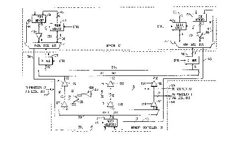
In Figure 1 is shown a block diagram of a portion of a
. computer system in which the shared memory controller
arrangement is uti1ized. Standard computer system elements
are processor 10, Qrocessor 11, system bus lZ, system memory
13, disk input~oucput device 14 and system pcocessor 15. ~n
the prior art processors 10 and 11 ~ould normally be
connected to system bus 12 along with systlm processor 1,
and.they would cooperate in a multiorocessing arrangement to
process application programs, with orocessoe 15 being a
master processor, in a well known manner.
In accordance with the teaching of the present invention
25 the two memocies 17 and 19 ace dedic3ted to the joint use oE
application-pcogr~m processors 10 and 11 to increase their
operating eEficiency, and to increase 'he efEiciency oE use
of melnories 17 and 19. ~emories 17 and 19 are respectively
associated wi~ ,ne~ory contro11er 16 and memory controller
30 18 which contro1 access to t'ne memories. ~cocessocs 10 and
11 are not connected dir-ctly to systeln bus 12, but c~tner
1 307352
1 are connected to a local bus 9. Memories 17 and 19 are also
not connected to the system bus 12. Also connected to local
bus 9 are tne memory controllers 16 and 18. Memory
controllers 15 and 18 primarily permit shared access ~o
their respective associated memories 17 and 19 by either
processor 10 oe processor 11. In this manner the chances of
ei~her processors 10 or 11 naving to wai~ to gain access to
a memory are statistically decreased compared to one memory
serving both processors.
~ emories 17 and 19 may also be accessed from system bus
12 via adapters 20 and.21 respectively to load application
programs and data to be processed into these memories ~or
subsequent use by processors 10 and 11. Similarly, memories
17 and 19 may be read out to circuits connected to system
bus 12.
In addition, processors 13 and 11 each have access via
memory controllers 16 and 18 and adapter ciccuits 20 and 21
respectively connected thereto to system bus 12 to gain
access to other storage circuits connected thereto such as
syste,n memocy 13 and disk I/O 14. The circuit details of an
exemplary memory controller 16 and a memory 17 are shown in
Figure 2 which is described further in this specification.
~5
There are ~our basic types (~, B, C and ~) of memory
read and write cransactions ~hat can be performed by the
invention working in the system configuration shown in bloc~
diagram form in Figure 1. In transaction tvpe A processor 10
3q ;nay read or write to ,nemory 17 associated with ,nemory
cont~oller 1~, processor 11 may read or write to memory 19
1 307352
1 associated with memory controller 18, processor 10 may read
or write to memocy 19 associated with memory controller 18,
and processor 11 may read or write to memory 17 associated
with memory controller 16. Access betwee.n processocs 10 and
11 and memory controllers 16 and 1~ for these type A
transactions is via local bus 9 and switches that are part
of memocy contcollers 16 and 18 and shown in ~igure 2. These
type A tcansactions never access other stocage ciccuits
connected to system bus 12.
There are also type ~ transactions wherein some circuits
connected to system bus 12, such as system pcocessor 15, may
request and gain access to memories 17 and 19 to write
programs or data therein for use by processors 10 and 11, or
to read processed data from these memories. A type 3
transaction request to access memory 17 associated with
memory controller 16 is always made via (recognized by)
adapter 20, and a re~uest ~o access me,nory 19 associated
with memory controller 18 is always made via (recognized by)
adaptec 21.
With type C tcansactions, processors 10 oc 11 can read
or write system memory 13 or other ciccuits connected to
system bus 12. To implement this type of. transaction
processor 10 must access only memory controllec 16, and
processor 11 ;nust access only memocy contcoller 18. When
memory controller 16 is seized by ~rocessor 10, controller
16 determines ic a memory or non-memocy address received
~rom processoe !0 is to nemory 17 and further deterinines if
memory 17 is to be accessed. Upon determining that Inemory 17
is not to be accessed, memory controller 16 forwards the
-- 6
1 307352
1 cead or write cequest via adapter 20 to system bus 12. After
memory controller 16 passes a read request to adapter 20 to
be placed on system bus 12, memory controller lÇ is not free
to service other read or write requests until the read
S operation to, for example, system memory 13 is completed.
~rite operations to, for example, system memory 13 are
considered completed as soon as the request, address and
data are passed to adapter 20, and memory controller 16 can
then process other read or write requests from either
processor 10 or 11. When the type C transaction request is a
read operation, the program oc data will be returned, and
can only be returned over the same path that the request is
made on. In addition, when adapter 20 receives the returned
program or data it must make an access request to memory
controller 16. That request is granted an appropriate
connection is established through .~emory controller 16 and
adapter 20 returns the data or pcogram to processor 10.
Thereafter, processor 10 is again free to request memory
read or write opecations from controllers 16 or 18.
Similarly, processor 11 can access system memory 13 or other
system circuits via its associated memory controller 18 and
adapter 21.
The D type transaction is d lock cycle transaction
wherein, ~or example, processor 10 can perform a read loc~
of either memory 17 or ,nemory 19, but the read operation is
not done dicectLy through memory controller 16. The loc~
operation, when callec for, assures that the addressed
me,nory from one processor will not acknowledge a bus cycle
initiated by another processor until the first pcocessor
operation is completed. Assuming ?rocessor 10 wants to do a
- 7 -
1 307352
1 read lock on memory 17, the address and read request sent to
memory controller 16 is not used to read memory 17, but
instead is passed to adapter 20. Adaptec 20 places t~e read
request and address on system bus 12 and then recognizes
5 that the address is to memory 17. Adapter 20 answers the
request it just placed on bus 12 and receives the read
request and address. Then adapter 20 makes a request Eoc
connection to memory controller 16 and memory 17. When that
request is granted, reading of memory 17 takes place. The
information read out of memory 17 is returned to adapter 20
rather than to processor 10. Adapter 20 takes the
information read out of memory 17 and destination and places
it on system bus 12. Adapter 20 then recognizes that the
information it just placed on bus 12 is for processor 10 and
re-captures the information. Adapter 20 again makes a
request for use oE controllee 16. r~hen this request is
granted, adapter 20 returns the inEormation via memocy
controller 16 and local bus 9 to processor 10.
Si.-nilarly, if ~rocessor 10 requests a read lock
operation to memory 19, the read request and address are
passed via memory controller 16 and adapter 20 to system bus
12 as desccibed in the last paragraph. However, adapter 21
recognizes that the read request is for ,nemory 19 and takes
the request and address Erom system bus 12. Adapter 21 makes
a request to memory controller la to read memory 19, anc
when the request is granted memory 19 is read. Like the cead
lock oper~tion desccibed in the last paragraph, t;-e
information re~d out of memory 13 is returned through memor~
contcoller 13 and adapter 21 to system bus 12. Adapter 0
recognizes tha~ tne inEormation on systeln bus 12 ia ~or
1 307352
1 processor 10 and stores the information. Adapter 20 then
makes a request for use of memory controller 16. When this
request is granted, adapter returns the information -~ia
controller 16 and local bus 9 to processor 10.
~ hile the type D read lock operation described in the
last two paragcaphs is initiated by processor 10 to either
memory 17 or memory 19, processor 11 can also request read
lock operation to memories 17 and 19 and the operation is
the same as that described in the last two paragraphs.
Furthermore, since the lock request is placed on system bus
12, a lock request of system memory 13 is performed in a
manner transparent to processor 10.
In Figure 2 is shown a detailed block diagram schematic
of a memory contcoller 16 and an associated me~ory 17. Since
controller 16 with memory 17 is the same as memory
controller 18 with memory 19, only the schematic of memory
controller 16 and memory 17 are shown in Figure 2 and are
described hereinafter.
Around the edges of the portion of Figure 2 identified
as memory controller 1~ are shown three input/output
connections to processor 10, to processor 11, and to adapter
which are shown in Figure 1. Each of these three
connections can carry information in both directions as
previously described with reference to Figure 1. In
addition, the connections between controller 16 and
associated mPmory 17 are shown. The three connections
identified in the beginning of this oaragraph are all
connected ~o a swi~cning network inplemented with buffer
1 307352
1 amplifiers 26 through 33. The data paths within memory
controller 16 are mostly thirty-two bit paths as indicated
by the slash mark and the number thirty-t~o adjacent
thereto, Accordingly, amplifiers 26 through 33 -ach
respectively represent thirty-two ampliEiers. Each of the
two-hundred fifty-six individual amplifiers represented by
amplifiers 26 through 33 are a 74S241 Tri-State Octal
Amplifier operated as a buffer driver in a manner well known
in the art. They are available from Texas Insteuments and
other sources.
~ he other circuits within memory controller 16 are word
selector 37 which has two sixteen bit inputs and a
thirty-two bit output. Word selector 37 is made up of eight
i5 Quad 2:1 Multiplexer chips designated 74A5157 which are also
available ~rom Texas Ins~ruments and other sources. Each o~
these chips is a ~our pole double throw switch. ~ord
selectoc 37 is used to reverse or transpose the two groups
of sixteen input bits at the output. That is, the sixteen
bits at the input from path 39 may be either the lower order
sixteen bits or the higher order sixteen bits of the
thirty-two bit output from translator 37. Similacly, the
sixteen bits at the input o~ translator 37 from path 40 ~ill
be the eemaining sixteen of the thirty-two bits output from
translator 37. ~ore detail o~ how this is accolnplished is
described further in this specification. Ciccuitcy analogous
to buffer ampli~iers 26 through 33 provide paths for
thirty-two address bits to/from processor 10, processor ll
or adaptec 20.
-- 10 --
- 1 307352
1 At the output of memocy controller 16 to memocy 17 are
two 2:1 multiplexers 35 and 36. Multiplexers 35 and 36 are
each made up of a number Oe 74AS2S7 multlplexers ha-~ing
tri-state outputs. That is, the output may be nigh, low or
open. Each of multiplexers 35 and 36 have thirty-two input
bits and sixteen output bits. These 2:1 multiplexers 35 and
36 are used to selectively choose which of the higher order
sixteen bits or lower order sixteen bits are to be applied
to the even memory 51 and odd memocy 52 in memory 17. In an
alternative embodiment of the invention memory 17 may be a
single memory instead of two smaller memories.
In the following paragraphs are described the routing of
data words within memory controller 16. The described
lS operations are the type A-D transactions mentioned
previously. After the routing of the data is described, the
qeneration of the CS control signals used to operate the
buffer amplifier switches within memory controller 16 is
described with reference to Figures 3, 4 and S.
When pcocessor 10 requests and gains access to memory
controller 16 for a read operation from memory 17, an
address is sent that is eirst checked. If the address is not
in the address range of memory 17, or is used in a lock
operation, read access is not granted Otherwise, cead
access is granted. In cesponse theceto a thicty-two bit wocd
is read out of memory 17 and input to memory controller 16
as sixteen bits on path 39 to one input of word selectoc 37
and sixteen bits on path 4C to the other input of word
selector 37 In response to a contcol signal CS input to
word selector 37 the two sets of sixteen input bits are
-- 11 --
1 3073~2
1 selectively connected to the higher ocder or lower order
sixteen-bits of the thirty-two bit output from word selector
.37.
The output from word selector 37 is connected to a
thirty-two bit MUXD bus 38 to which also are connected the
inputs of buffer amplifier switches 27, 31 and 32. For the
read operation from memory 17 a control signal CS2 is
generated which operates the thirty-two individual
amplifiers making up buffer amplifier 27. This connects the
thirty-two bit word read from memory 17 to input/output path
53 to be returned to processor 10.
Alternatively, if processor 10 is writing to memory 17,
a thirty-two bit word is presented on ihput/output path 53.
A contcol signal CS1 is generated which operates the
thirty-~wo individual amplifiers making up buf~er ampli~ier
26. Thus, the thirty-bit word on input/output path 53 is
connected to MDTI bus 34. Multiplexers 35 and 36 have their
inputs connected to MDTI bus 34 and control signals are
applied to them to select which of the higher order and
lower order slxteen-bits o~ the thirty-two bit word on bus
34 will pass through 2:1 multiplexers 35 and 36 and be
stored in even memory 51 and odd memory 52 of memory 17.
In an operation where processor 11 requests and gains
access to memory controller 16 to read ~rom memory 17, tne
thirty-two bit word read out o~ memory 17 a?pears as
sixteen-bits on ?ath 39 and sixteen-bits on ?ath 40. As
described above these two sets o~ sixteen bits are
selectively transQosed by word selector 37 and are present
1 30735~
1 on MUXD bus 38. A control signal CS4 is genecated which
operates each of the thirty-two amplifiers making up buffer
amplifier 32 to connect the thirty-two bit word read out oE
memory 17 to input/output 54 path and on to processor 11.
s
If instead processoc 11 is writin~ to memocy 17, aftee
the orocessor requests and gains access to memory controllec
16, a control signal CS3 is generated whicn operates each of
the individual amplifiers comprising buffer amplifier 33 and
connects the thirty-two bit word to be written into memory
17 to MDTI bus 34. As previously described other control
signals operate 2:1 multiplexers 35 and 36 to selectively
apply the higher order and ~lower order sixteen-bits of the
word to be stored to even memory 57 and odd memory 52 of
memory 17.
In a type B transaction a circuit connected to system
bus 12, such as system processor 15 or syste,n me;nory 13,
requests access to memory 17 to either read data from this
memory, or to store othec dat~ or programs in this memory
for use by processor 10 in future processing. When system
processor 15 wants to write into memory 17, it first gains
access to adapter 16 or 18 and transmits to it information
to be written and an address in memory 17. Adapter 20 in
turn requests access to memory controller 16 to write into
memocy 17. When this r-quest is granted, a contr~l signal
CS7 is yenerated which operates the thirty-two ampliEiers
making up buff?r ampliEier 30. A ~nirty-two bit word Ecom
adapter 20 present on input/output !)ath 55 is ~hereb~
connected to ~l~TI bus 34. As previously described 2:!
multiplexers 3S and 36 are ooerated to selectively place t~.?
- 13 -
1 30735~ .
1 higher order and lower order sixteen bits of the thirty-two
bit word from adapter 20 into even memory 51 and odd .ne,nocy
52.
To read memory 17 to adapter 20 and thence to a circui~
connected to system bus 12, memory 17 is addressed and cead
out via paths 39 and 40, and word selector 37 to MUXD '3US
38. Control signal CS8 is generated that enables t.he
thirty-two amplifiers rnaking up amplifier 31 to connect the
thirty-two bit word read out to input/output 55 path and via
adapter 20 to system bus 12.
In an operation where processor 10 requests and gains
access to memory controller 16 to be connected via adapter
lS 20 and system bus 12 to other storage circuits, sucn as
system memory 13, different contcol signals are generated
When .his t~pe ~ ~ransaction ia' a ~rite operation, cont~ol
signal CS5 operates buffee amplifiers 28, and the data word
present at input/output 53 is passed through to input/output
path 55 and to adapter 20. As previously described adapter
20 will gain access to system bus 12 and will store the data
word from processor 10 in the requested storage circuit.
In a type C transaction where processor 10 is reading
ZS from a storage circuit, such as syste,n memory 13 connec~ed
to system bus 12, processor 10 ~irst requests and then gains
access to memory controller 16. The connection to adapter 20
is tAe same as described in the last oaragraph and the read
request and address are passed to adap~er 20. The connection
between processor 10 and memory controller 16 is then
broken. As pr-viously described, controller 16 can noh
- 14 -
1 307352
l handle read/write requests fcom processoc ll, but processor
lO cannot request any other read or write operations with
controller 16, or controller 18 until the present read
operation from a system storage circuit on system bus 12 is
S completed.
When the read operation requested by processor lO has
been accomplished by adapter Z0, this adapter makes a
request for access to memory controller 16 and indicates
that it needs a connection to processor 10. When the access
request by adapter 20 is granted, a control signal CS6
operates buffer amplifiers 29. This passes a data word on
input/output path SS from adapter 20 ~ directly to
input/output path 53 and thence to processor 10.
Type C transactions involving processor ll are not
handled by controller 16; instead, processor 11 uses
contcoller 18 to access adapter Zl. The details of such type
C transactions involving processor ll are identical (except
for the designations) to those outlined in the previous two
paragraphs.
~ hirty-two bit word memory 17 is made up of two
sixteen-bit memories Sl and 5Z in the preferred embodiment
of the invention. However, a single thirty-two bit word
memory.may also oe used with minor changes in the erroc
circuit which is well known in the act. Memory 51 is the
even memory and memory 52 is the odd memory as descriDed
?reviously. Data or program instructions to oe stoced in
even memory 51 aee switched through memory controller 16 to
even data bus 41, and then over path 43 to the input of even
1 307352
1 memory 51. Memory 51 dlso has an address applied thereto and
a read/write indication that are not shown but which are
well known in the art. The operation of memory 51 in
response to such si~nals is also well known in the art. When
memory 51 is being read rather than written, there is no
data on Qath 43.
Information read out of even memory 51 is twenty-two
bits wide, sixteen bits of which are the information of
interest, and six bits of which are an error correction
code. The sixteen information bits read out of even memory
51 are connected to the inputs o~ buffer am~lifier 45.
Amplifier 45 is made up of sixteen individual amplifiers,
and are implemented with Fairchild 74F373 Tri-State Octal
Registers operating as buffer amplifiers. auffer amplifier
45 is controlled by control signal CS9, which is generated
and applied to amplifier 45 onl~ when even memory 51 ia read
out.
The si~ error correction bits read out of even memory 51
during a memory read operation are input to error circuit
47. The sixteen information blts read out of even memory 51
are switched through buffer amplifier 45 to even data bus 41
and are input via path 56 to error circuit 47. This makeup
of sixteen information bits and six ecror correction bits is
a standard 16/6 Hamming code that is well known in the art.
Error circuit 47 is an AI~D2960 erroc correction and
detection chip available ~com American Micro-Devices, and is
operated in a standard manner. Error circuit 47 prPcesses
the sixteen bit data word present at its input to check ~or
and correct errors in the sixteen bits, if at all ?ocsible.
- - 16 -
1 3~7352
1 The checked and/or corrected sixteen bit information word is
output from error circuit 47 back onto path 56 to even data
bus 41. This infocmation word then flows from bus 41 onto
path 39 back into memory controller 16 to word selector 37
as previously described.
While the memory circuit operation described in the
previous paragraphs is for even memory 51, the same
described operation applies to odd memory 52. Accordingly,
the operation is not again repeated with reEerence to odd
memory 52.
In Figure 3 is shown a simple block diagram of a tie
breaker circuit 58. There are two tie breaker circuits, one
lS associated with each of memory contcollers 16 and 18. Tie
breaker circuit 58 shown in Figure 3 is associated with
processor 10. That is, in Figure 3 the lowest priority
request is from processor 10, but in the second tie breaker
circuit (not shown) the lowest priority request is from
processor 11. In addition, the A and B suffixes on the A and
8 request and grant signals are reversed. That is, for
example, an Ac3apter A request becomes an Adapter B request.
Tie bceaker c:ircuit 58 is ~ell known in the art and is
taught in U.S. patent 4,493,036, having the same assignee as
the present invention. The material in this earlier patent
is not repeated herein to avoid detracting from the present
in~ention, and because it does not form part of the
invention.
3~
1 307352
1 The description of the tie breaker circuit 58 shown in
Figure 3 is made with this circuit being assigned to grant
requests for access to memory controller 16. There are four
request inputs to tie breaker 58. ~hey are a ~10 request
~rom processor 10, a ?11 request from processor 11, an
Adapter A request from adapter 20, and a Refresh request.
Even though circuit 58 is associated ~ith orocessor 10,
processor 10 is assigned the lowest priority access tO
memory controller 16. The highest priority is assigned to
the Refresh request. Memory 17 is an NMOS memory, well known
in the art, and in operation charge slowly leaks off and
must be replaced or refreshed or the contents of memory 17
are lost. Since i~ cannot be permitted to lose the contents
of memory 17, its contents are periodically refreshed.
memory refresh circuit is not shown or described since they
are well known in the art, but a refresh request ~rom same
receives the hiqhest priority to ~ccess memory controller
16 and refresh memory 17.
Adapter 20 is assigned the second highest priority to
access memory controller 16. ~his higher priority is
assigned because on a relative basis adapter 20 is seldom
requesting access to ,nemocy controller 16, but when it does
it needs priority access to place programs or data in memory
17 ~or use ?rimariiy by orocessor 10, or to read the resul,s
of previous processing from memory 17.
Similarly, orocessor 11 seldom requests access to memory
controller 16 w~en compared to access by ?rocessor 10 so i_
has been given ~ nigher ?riority than pcocessor 10.
1 307352
1 In operation of tie breaker 58, when memory controller
16 is idle the first of the four requests to appear at the
inputs of circuit 58 is immediately granted. However, if two
requests from a ~irst and a second circuit appear
simultaneously, the request from the circuit having the
higher priority is first granted access to memory controller
16. When the first circuit to which the access has been
granted is finished with a read or write operation ~he
request feom the second circuit is granted. If while the
first circuit has access to memory controllec 16 a third
circuit requests access to controller 15, tie beeaker
circuit 58 will then select between the second and third
circuits requesting access and the one of these two circuits
having the higher priority will be granted access to memory
lS controller 16 ~ollowing the first circuit.
There is also an End of Cycle input to tie ~reaker
circuit 58 which has a signal from a system clock or tim-ng
circuit, not shown but well known in the art, which
indicates the end of the current melnory controller cycle.
This timing signal restarts ciccuit 58 to make another
decision and grant access to mernory controller 16 if any
requests are awaiting service.
'~hichever access requesting circuit is geanted access to
memory controller 16 by tie breaker çircuit 58, it has its
associated ~equest Granted output lead go high. For example,
if ?rocessoc 10 requests connection ~o memory controller 16
and 'he reques is granted, the Processor 10 Granted output
from tie breakee circuit 58 goes high. he request granted
out~uts ~rom tie breaker ciccuit 58 are input to a control
-- 19 --
1 307352
1 signal generator circuit shown in Figure 4. Although not
specifically shown in Figure 3, the request granted outputs
-from tie breaker circuit 58 are also connected back to their
respective access requesting circuits so that the requesting
circuits receive an indication when their request is granted
and they are connected to memory controller 16.
In Figure 4 is shown the control signal generator
circuit which responds to the access granted signals output
L0 from tie breaker circuit 58 to generate CS control signals
that operate the switching buffer amplifiers shown in Figure
2 and described previously in this specification. There is a
control signal generator circuit associated with each memory
controller, and the circuit shown in Figure 4 is associated
15 With rnemory controller.16. The control signal generator
comprises an equality detector 60 and a orogrammable arcay
logic (PAL) circuit S9. In addition to the inputs from tie
breaker circuit 58, there is also a R/W operation input on
which is a signal indicating if a read or a write operation
is to perfocmed on memory 17 or another storage device
connected to system bus 12 in Figure 1. There is also a
Non-Memory Operation input that indicates i~ the requested
read or write operation involves memory 17 or one Oe the
other system stora~e devices. Finally, there is a valid
address input fro,n equality detector 60 that lndicates if
the memoey address forwarded to memory controller 16 can oe
used to address memory 17. Path selection in memory
controller 16 is by means of CS enable signals generated ~y
circuit 59.
- 20 - -
1 30735~
1 More specifically, equality detector 60 is a 74~521
equality detector comparator available erom ~airchild
Semiconductor. The PAL is available from numerous sources
and is programmed to provide outputs for specified input
signal combinations in a manner well known in the art. The
input and output signal relations are shown in Figure i and
permit programming of PAL 59 to implement the control signal
generator. One input to detectoe 60 is the memory address
froln processoc 10. The other input to detector 60 indicates
the range of addresses that can be addressed in memory 17
and can be supplied by settings on DIP switches as is well
known in the computer art. Detector 60 compares an address
from processor 10 with the range of addresses of memory 17.
If the address fro,n processor 10 is within range, there is
an appropriate output from detector 60 indicating same.
Howevec, an output from detector 60 indicating that the
address is in range or valid doesn't alone mean a read or
write operation will be performed with memory 17. The
address may also be valid for a storage device such as Disk
I~O 14 connected to system bus 12 in Figure 1. Accordingly,
the control signal generator also needs another input
indicating if the requested read or write operation is to
involve memory 17. The other input is ~he Non Memory
Operation input which has an indication thereon only if tne
read or write operation involves memory 17. The lack of an
indication oo the Non i~emory Operation input or the lack of
an Address OK signal from detectoc 60 indicates that the
requested o~eration is to another storage de~ice connected
to system bus 12.
- 2L -
1 307352
1 When processoc ll requests and receives access to memory
controller 16, the address it focwards is not checked
because processor 11 can never establish a connection
through memory controller 16 and adapter 20 to perform a
S read or weite operation involving a storage device connected
to system bus 12.
In Figure 5 is shown a logic table showing the state of
inputs to the control signal generator (PAL) 59 to get the
indicated CS control signals that are used to operate the
switching buffer amplifiers shown in Figure 2. This
information enables one s~illed in the art to program PAL
59 .
While what has been described hereinabove is the
preferred embodiment of the invention, it should be
understood tnat numerous changes may be made without
departing from the spirit or scope of the invention. Foe
example, memory 17 may be a single memocy rather than the
even or odd memories disclosed. ~n addition, the number of
processors, memory controllers and memories may be
increased.
.