Note: Descriptions are shown in the official language in which they were submitted.
:~L3~7939
METHOD OF ADJUSTING BRIDGE CIRCUIT ~F SEMIC()NDUCTOR
PP~ESSURE SENSOR
BACKGROUND OF THE INVENTION
This invention relates to a method of adjusting a
bridge circuit of a aemiconductor pressure sensar under
the wafer process and more specifically to a method of
adjusting a bridge circuit of ~I semiconductor pressure
sensor typical of a semiconduc1:or pressure sensor fitted
to the tip of a catheter for medical use.
When a mechanical stress is applied to a semiconductor
crystal of silicon or the l.ike, its resistance.changes
greatly because of the piezoelectric resistance effect
t and the perception of this :Eact has led to the development
of a semiconductor pressure sensor. The process of makiny
such a semiconductor pressure sensor comprises the steps
~ of formung a st~n gauge resis~r by diffusion of impurity ions on the
~ace layer of a silicon single crystal, as.sembling~four .'
of the strain gauge resistor.s into a Wheatstone bridge,
: forming a recess in the back surface of the silicon
: monocrystal by etching, and disposing electrodes in
suitable places on the surface thereof with the thin
portion as a disphragm. When pressure is applied to the
semiconductor pressur~ sensor, the diaphragm is deformed
and the resistance value of the strain gauge resistor
changes to a greater extent because of the piezoelectric
~k
. ~ .
:
~ ,.
7939
1 resistance effect, so that a bridge output proportional
to the pressure is obtainable.
The aforesaid semiconductor pressure sensor is
extremely small in size and, particularly in the case of
a semiconductor pressltre sensor for medical use, a
plurality of semiconductor pressure sensors are fitted
to the tip of a catheter and inserted into a body.
Accordingly, even in a semiconductor pressure sensor
incorpora~ing peripheral circuits such as a temperature
compensating circuit, a pressure sensitivity compensatillg
circuit and the like, a side of a chip should be about
1 mm or smaller in length.
Variations in resistance value of each of the strain
gauge resistors and diffused resistors at their formation
and uninformity in the thickness of the diaphragm produced
by the etching process resu].t in variations in the
characteristics of the semiconductor pressure sensorO
However, the semiconductor pressure sensor i5
e~tremely small in size and it is very difficult to
measure the electrical characteristics while pressure is
being appl1ed actually and adjust the resistance balance
of the bridge circuit. Actually, the measurement of
such electrical characteristics while the pressure i5
being applied is omitted, whereas only the electrical
characteristics of the bridge circuit are measured to
., .
.
~ "
~3~7~39
1 find and discard what exceed a predetermined tolerance
as inferior goods.
Accordingly, yields of the semiconductor pressure
sensor are poor and, in addition to this problem, the
measurement of electrical characteristics has posed lack
; of reliability because the degree of deformation of the
diaphragm resulting from the pressure actually applied
thereto is not measured.
SUM~ARY OF THE INVENTIO~
In view of the aforesaid problems, an object of the
; pr~sent invention is to provide a method of adjusting a
bridge circuit of a semiconcluctor pressure sensor to
improve yields by adjusting the output balance of the
bridge circuit based on the output of the semiconductor
pressure sensor in a state c:losely approximated to that
wherein the semiconductor pressure sensor i5 actually
in use.
In order to accomplish the aforesaid object, the
method of adjusting the bridge circuit of a semiconductor
pressure sensor comprises the steps of forming the
principal part of the bridge circuit consisting of strain
gauge resistors and diffused resistors connecting the
strain gauge resistors during the diffusion process of
a diaphragm type semiconductor pressure sensor, providing
conductive 11nP~ connected to at least one of
~L3~7~33g
1 the diffused resistors at predetermined intervals during
the wiring process, providing an Al pad common to the
ends of the conductive lLnes, mRking vacuum suction to the back
surface of the diaphragm in the testing process to create
a state wherein press~lre is virtually applied to the
diaphragm from the surface side thereof, measuring the
pressure sensitivity of the semiconductor pressure sensor
from the surface side of the diaphragm by making use
of the bridge circuitl and selectively cutting the
conductive lines based on the pressure sensitivity
thus measured to adjust the output balance of he bridge
circuit by adjusting the resistance value of the diffused
resistor~
On the other hand, during the wiring process, pads
may be installed at the erLds of respective conductive
7;nes and one of the pads may be
selected and bonded based o~ the pressure sensitivity
: of the semiconductor pressure sensor to adjust the output
balance of the bri~ge circuit~
In the method of adjusting the bridge circuit of a
semiconductor pressure sensor, the diaphragm issubJected to vacuum
suction from its back surface side to subject the diaphragm
to negative pressure during the testing process and
the resistance value of the strain gauge resistor forming
the principal part of the bridge circuit fo~med on the
.
- 4 -
:.
,. ' ~ ` ' :
.,
.
~3~g39
1 diaphragm is caused to change through the deformation of the
diaphragm and the piezoelectric resistance effect.
The changes in the output of the bridge circuit can be
measured by making use of the electrodes formed on the
surface of the semiconductor prlessure sensor.
The resistance value can be set stepwise by providlng the
- lines connected tothe dif~used resistor at the predetermined
intervals and the diffused resistor is distributed by
selectively cutting the lines or bonding one pad whereby
the resistance value can simply be ad]usted.
Accordingly, before the wafer is diced, ii is
possible to adjust the brid~e circuit of the semiconductor
pressure sensor readily by adjusting the resistance balance
of the bridge circuit while pressure is being applied
thereto.
BRIEF DESCRIPTION OF THE DRAWINGS
Fig. 1 is a schematic top view showing a method of
adjusting a bridge circuit of a semiconductor pressure
sensor according to a first embodiment of the present
invention.
Fig. 2 is a cross sectional view of the semicondu~tor
pressure sensor of Fig. 1.
Fi~o 3 is a schematic sectional view showing an
embodiment for measuring the pressure sensitivity of
the semiconductor pressure sensor.
,
~3~793g
l Fig. ~ is a diagram showing a state wherein pressure
is applied to the semiconductor pressure sensor.
FigO 5 is an electric circuit diagram showing an
electrical arrangement of the semiconductor pressure
sensor of Fig. lo
~; Fig. 6 is a schematic top view showing a method of
adjusting a bridge circuit of a semiconductor pressure
sensor according to a seccnd emxX~nent of the present invention.
Fig. 7 is a cross sectional view of the semiconductor
pressuxe sensor of FigO 6.
Fig. 8 is an electric circuit diagxam showing an
electrical arrangement of the semiconductor pressure
sensor of Fig. 6.
DETAILED DESCRIPTION OF THE PREFERRED EMBODIMENTS
Referring now to the accompanying drawings, embodiments
of the present invention will be described in detail.
Fig. 1 is a schematic ~op view showing a method of
adjus~ing a bridge circuit of a semiconductor pressure
sensor according to a first embodiment of the present
invention~ Fig. 2 is a schematic cross sectional view
of the semiconductor pressure sensor. In Figs. 1 and 2,
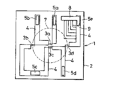
a semiconductor pressure sensor 1 is extremely~small
with a thickness of about 400 um and p~ type strain gauge
resistors 3a, 3b, 3c, 3d of several kQ are formed on
the surface of a substrate 2 composed of an n~ type
~3~7~3~ ~
1 silicon single srys~. Four of the strain gauge resistors
are wired in sexies using p~ diffused resistors 4
which are - extended around the surface
of the substrate 2 and AQ pads 5a, 5b, 5c, 5d, 5e are
formed on the diffused resistors 4 thus extended. Moreover,
a recess 6 is formed in the back surface of the silicon
single crystal 2 with a thin portion ~with a thickness of less
than 30um) used as a diaphragm 7.
In addition to the construction of the aforesaid
known semiconductor pressure sensor 1, an AQ pad 8 is
installed and lines 9 of an electric conductor ~for
example, aluminum,gold, silver, copper, etc.~ are provided to be
! connected to the diffused resistor 4 wired between the AQ
pad 5e and the strain gauge resistor 3d at predetermined
intervals. The ends of the all lines 9 are connected to
the AQ pad 8.
The AQ pads 8 and 5e are connected and further the
AQ pads 5e and 5a are connected. Voltage is applied
across the AQ pads 8 ~5e) and AQ pad 5c to obtain an
output between the AQ pads 5b and 5d. That is, a bridge
circuit is arranged (see Fig. 5). In Fig. 5, r1 ~ r8
represent the resistance values of the diffused resistors
4. The adjustment of the output balance of the bridge
circuit is made by selectively cutting the lines 9
by a laser beam and adjusting the resistance value ~r~l
~3~793~
1 between the AQ pad 5e and the resistor 3d.
The intervals at which the lines 9 are connected to
the diffused resistor 4 are set according to the resistance
characteristic (Q - m) of the resistor and, provided the
resistance characteristic is linear, an equal interval
is preferred~
The present invention is not limited to the afoxesaid
embodiments. The AQ pads 5a ancl 5e are connected, for
instance, and voltage is ap~lied across the AQ pads 8
and 5d, whereas the resistance value of not only the
diffused resistor 4 between the AQ pad 5e and the straih
; gauge resistor 3d but also those of other diffused
resistors may be made adjust:able, provided the combination
and arrangement of parts are modified without departing
from the ~prit and the scope of the invention as
hereinafter claimed.
FigO ~ is a schematic t;op view showing a method of
adjusting a bridge circuit of a semiconductor pressure
sensor according to a second embodiment of the present
invention. Fig~ 7 is a schematic cross sectional view
of the semiconductor pressure sensor of Fig. 6. This
embodiment is substantially the same as what is shown
in FigO 1 except that AQ pads 8' are connected to the res~ective
conductive lines 9.
In this embodiment, the AQ pads 5a and Se are
,`'; :'
. ~
~3~7939
1 connected and voltage is applied across the A~ pads 5a,
5e and the A~ pad 8', whereas an output is taken out
from between the AQ pads 5b and 5d. That is, a bridge
circuit is thus arranged and any one of the AQ pads 8'
is properly selected ?.nd bonded for the purpose of
adjusting the resistance value r4 (r5) of the di~fused
resistor 4 formed between the strain gauge resistors
3c and 3b as the wiring (see Fig. 8)o In Fig. 8, r
r8 represent the resistance values of the diffused
resistors 4.
A resistance adjusting circuit 110 in this embodiment
may be arranged between not only the strain gauge resistors
3b and 3c but also other strain gauge resistors to effect
the adjustment of the diffused resistors 4. Moreover,
the intervals at which the :lines 9 are connected to the
diffused resistor 4 are set according to the resistance
characteristic (Q - m) of the resistor and, provided
the resistance characteristic is linear, an equal interval
is preferred.
Fig. 3 is a sch matic sectional view showing an
example for measuring the pressure sensitivity of the
semiconductor pressure sensor, wherein a wafer stage 10
has a vacuum leakage ~reventing seal material 12 of
soft synthetic resin ~for example, styrene, butadiene
or silicone ruhber) with a thickness in the order of
_ g _
,,, ~ . .. ~., '
~ . ....
.~
~` ~3~793~
1 10 um, which is formed on a plate material 11 of stainless
or synthetic resin. Further, at least one through-hole
13 is bored in a suftable place of the wafer stage 10 to make
vacuu~-suction to a recess 6 of the semiconductor pressure
sensor 1. The recess 6 of the semiconductor pressure
sensor 1 is located above the through-hole 13. In the
first embodiment shown in Fig. 1, the measuring probes 14
are caused to contact across the AQ pads 5a, 5e and th~
AQ pad Sc (between the input terminals of the bridge)
ancl across the AQ pads 5b and 5d (between the output
tel~inals thereof) provided on the surface of the
semiconductor pressure sensor 1. In the second
en~odiment shown in Fig. 6, the measuring probes 14 are
caused to contact across the AQ pads 5a, 5e and the AQ
pad 8' (between the input terminals of the bridge) and
across the ~Q pads 5b and Sd (between the output terminals
thereof)~
In order to locate the recess 6 of the semiconductor
pressure sensor 1 above the through-hole 13 of the wafer
stage 10, the wafer 15 should be moved while the wafer
stage 10 and the measuring probes 14 are set still or
the wafer stage 10 and the measuring probes 14~should
be shifted while the wafer lS is set still.
As set forth above, the wafer 15 is mounted on
the wafer stage 10 and is subjected to vacuum suction using the through-
- 10 -
. .... ~.
,~
' ~ '
,
~3~ 3~ ~
l hole 13 and the seal material on the wafer stage 10
prevents vacuum leakage through the connection between
the silicon crystal 2 and the wafer stage 10. Moreover,
the negative pressure corresponding ~o the pressure
applied from the surface of the semiconductor pressure
sensor 1 is generated at the recess 6 and the diaphrasm 7
is deformed as in the case where the pressure is applied
thereto trom the surface.
Fig. 4 is a schematic view showing the diaphragm 7
thus deformed. ~he strain gauge resistors 3a and 3c
formed by diffusion in the center of the diaphragm 7
out of the four strain gauge resistors 3a, 3b, 3c and 3d
! constituting the bridge ~ircuit as shown in FigO 5 or 8,
are compressed, whereas the strain gause resistors 3b
; 15 and 3d diffused on the periphery of the diaphragm 7 are
extended as the diaphragm 7 is deformed.
With respect to the strain gauge resistors, use is
made of those whose resistance value increases propor~
tionally to the stressO Given the resistanoe
values of the strain gauge resistors 3a, 3b, 3c and 3d
respectively at Rl, R2, R3 and R4, R2 and R4 increases
whereas Rl and R3 decreases as the diaphragm 7 deforms.
In other words, the potential Vl acrojs the terminals of the
resistor 3b increases, whereasthe potential V2 across the
terminals of the resistor 3c decreases.
-- 11 --
13~7~3~
1 Accordingly, the bridge output, i.e., V1 - V2
increases in proportion to the deformation of the
diaphragm 7.
The pressure sensitivity of the semiconductor pressure
sensor l can be measured, before the wafer 15 is diced,
by measuring the bridge output with the measuring probe
14 using the AQ pads of the semiconductor pressure sensor 1.
The output of the semiconductor pressure sensor is
measured while the pressure is being applied thereto.
With respect to the semiconductor pressure sensor whose
me.~sured value shows a slight error, the
lines connected to the diffused resistor 4
are appropriately cut out by a
la3er beam (first embodiment), or otherwise one of the
AQ pads 8~ provided at respective lines 9 connected
- to the diffused resistor 4 at the predetermined intervals
is selected (second embodiment), whereby the resistance
vaLue of the diffused resistor can ~e easily adjusted.
Therefore, the output balance of the bridge circuit of
the semiconductor pressure sensor can be adjusted before
the semiconductor pressure sensor is diced~
In a brief summary, the electrical measurçment is
made from the surface side of the semiconductor pressure
sensor 1 and the pressure is applied from the back
surface side thereof, whereby the pressure se~sitivity
- 12 -
.
. .
~3(:?7939
1 of the sem.iconductor pressure sensor 1 is measured under
the testing process. With respect to the semiconductor
pressure sensor showing error in the measurement, the
output balance of its bridge circuit can be adjusted by
adjusting the resistance value of the difused resistor 4.
As set forth above, in the method of adjusting the
bridge circuit of the semiconductor pressure sensor
according to the present invention, there is created a
state in which pressure is virtually applied to the
diaphragm from the back surface side of the semiconductor
pressure sensor and the electrical output is measured
in that state similar to that of actual use. Then
the lines connected tothe diffused resistor
at the predetermined intervals
are suitably cut out or otherwise one of the
Al pads provided at the respective lines connected
to the diffused resistor at the predetermined
intervals is properly selected and bonded so that the
balance adjustment of the bridge circuit of the
semiconductor pressure sensor can be made by adjusting
the resistance value of the diffused resistor.
Accordingly, yields of the semiconductor pressùre sensor
are improved.
- 13 -
~3~7939
1 ~lthough, in the above described embodiments,
recesses 6 provided in the wafer 15 are subjected to
vacuum suction one ~y one, all recesses may be subjected
to vacuum suction simultaneously by providing a porous
member, through which a gas can pass, between the wafer 15
and the wafer stage 10 provided the through-hole 13.
Also, in the above described embodiments, although
one resistance value of a diffused resistor is adjusted,
. any resistance values of any diffused resistors may be
adjusted.
-14-