Note: Descriptions are shown in the official language in which they were submitted.
` 35317
`` ~3081~
B~CKGROUND OF THE INVENTION
Field of the Invention
This invention relates generally to an electronic
still camera and, more particularly, to a power supply
circuit for an electronic still camera having a flash
generating device.
Description of the Background
In a so-called electron-c camera, information
relating to an image formed by the lens is converted into
electrical signals and magnetically recorded on a magnetic
record medlum. In such camera, it i9 generally not required
to supply power to both an image-producing portion and to a
recording portion at the same time, for example, to a motor
for driving a magnetic disc at the same time the focus of
the lens ls being adjusted. Therefore, there is usually an
operating member provided to enable a first switch and a
second switch to be closed in turn, 80 that when the first
~witch is closed by the operating member power is supplied
to both the image-producing portion and the recording
portion, whereby preparation fo~ rotating the magnetic disc
by the motor i8 made, the condonser used for generating
flash is charged, and so on. Then, the second switch i8
clo~ed, information of a desired image is magnetically
recorded on the magnetic disc.
In the above-described electronic camera, however,
when the first switch is closed, preparations for driving
the motor and charglng the condenser are slmultaneously
-,
,
, , : :
.. s~ ~
8 ~61 353l7
made, as represented in Fig. 5B. Fig. 5B graphically
represents a time-current relation for the various
operations, and shows that a concentrated charging current
cannot be supplied to the main condenser for charging -it in
a relatively short period of time. Thus, the charging
period for th~ condenser is unduly prolonged. Furthermore,
a large changing current, for example, about lOA transiently
flows for the duration of charging, particularly at the
initial stage of charging, so that the voltage available for
application to a signal processing circuit of the camera is
reduced to an unacceptable level. Therefore, because of
this voltage reduction, malfunctions of the signal
processing circuit of the camera are apt to occur.
OBJECTS AND SUMMARY OF THE INVENTION
Accordingly, it i8 an object of the present
invention to provide an electronic camera that can eliminate
the above-noted defects inherent in the prior art.
It is another ob~ect of the present invention to
provide an electronic camera in which a current supplied to
a motor for driving the magnetic disc is interrupted while
charging the flash generating circuit, so that a large
charging current is available for the duration of charging
the flash generating portion and 80 that the time required
for charging can be lessened.
A further object of the present invention is to
provide an electronic camera in whlch currents are not
supplied to all signal processing circuits, including a
-2-
~3~8~6~ 35317
recording circuit as well as the motor for driving the
magnetic record medium, for the duration of charging the
flash generating portion, so that the signal processing
circuit is prevented from erroneous functioning due to
source voltage drops caused by the charging operation.
In accordance with an aspect of this invention,
an electronic camera comprises an image-producing element
and a signal processing circuit for converting output
signals from the image-producing element into recordable
electronic signals suitable for recording by a record
medium. A motor is provided for rotating the record medium
and a flash generating circuit has a charging circuit
capable of saving electric power that is requisite for
producing the flash. ~ power supply supplies power to the
motor and to the charging circuit, and a controller controls
the power supplied to the flash generating circuit and to
the signal processing circuit. Furthermore, in an
electronic camera according to the present invention, the
power is prevented rom being supplied to the disa-drive
motor by the controller for the duration of the charging
operation.
In accordance with another aspect of the present
invention, the power is prevented from being supplied to the
disc-drive motor and also to the signal processing circuit
by the controller for the duration of the charging
operation.
Therefore, in an electronic camera in accordance
with the present invention a large charging current is
-3-
}
" ' , '' " '' , .
~ .
:
.. . .
; ~3~8161 35317
available in the flash generating portion for the duration
of the charging operation, even though a source voltage drop
is developed due to such charging, and any low voltage
caused by the changing operation is prevented from being
supplied to the signal processing circuit of the camera.
The above and other objects, features, and
advantages of this invention will be apparent from the
following detailed description of illustrative embodiments
thereof to be read in connection with the accompanying
drawings, wherein like reference numerals identify the same
or corresponding parts in the several views.
BRIEF DESCRIPTION OF THE DR~WINGS
Fig. 1 i8 a partially exploded, perspective view
of an electronic camera according to an embodiment of the
present invention;
Fig. 2 is a perspective view of the electronic
camera of Flg. 1, shown with a record medium cassette;
Fig, 3 is a schematic in block diagram form of the
operable elements of the electronic camera of Fig. l;
Fig, 4 is schematlc in block diagram form of major
element~ of the electronic camera of Fig. l;
Fig. 5A is a graphical representation of a
time-current relationship present in the electronic camera
of Fig. l; and
Fig, SB is graphical representation of a
time-current relationship present in a conventional
electronlc camera.
13~81~1 35317
DET~ILED DESCRIPTION OF PREFERRED EMBODIMENTS
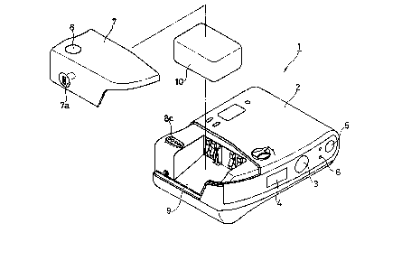
In Fig. 1 an electronic camera 1 is shown that
embodies the present invention, in which images produced by
lenses are converted into electrical signals by an image
sensor unit, such as a CCD, and recorded on a magnetic disk.
More specifically, a camera body 2 has in a front surface a
lens 3 for focussing the images, a flash 4, and a viewfinder
5. A photoelectronic device 6 incorporated in a circuit
described below for measuring the intensity of the light
that is reflected from an object is arranged on the front
surface of camera body 2. A photo transistor, which has a
good response to light, is often used as photoelectronic
device 6. The operation of the flash unit is controlled in
correspondence with the output of the photoelectronic device
6, and the light radiation ceases as soon as the amount of
light reaches a proper level.
A recess 9 into which a battery unit 10,
comprising secondary batteries or dry batteries, acting as a
power source, i8 formed in the left top side of camera body
2, and a cover 7 for covering recess 9 is detachably secured
to camera body 2 with a fastener 7a. A shutter-release
button 8 disposed in cover 7 closes in turn first and second
contacts of switch 8c when depressed.
When the first contacts of switch 8c are closed,
power is supplied to an image-producing portion 15, a
recording portion 16, a flash generating clrcuit 17, etc.,
as shown in Fig.3. As a result, the light reflected from
the object to be recorded is measured and the
~ 1 3 08 ~61 35317
image-producing portion 15, the recording portion 16, etc.
are placed in respective stand-by states.
When the second contacts of switch 8c are closed,
signals representing the image are recorded on the magnetic
disk 12. It is to be noted that the shutter-release button
8 is biased in a direction to protrude from camera body 2
due to the force of a spring, not shown.
As shown in Figure 2, formed in the rear of camera
~; body 2 is a cassette insertion opening ll, through which a
disk cassette 13 that internally accommodates a rotatable
magnetic disk 12, shown in phantom, is inserted. A socket
14 having input terminals is also provided in the rear of
the box 2, and power can be supplied through socket 14 when
a suitable plug connected to a reproducing apparatus (not
shown) is inserted in socket 14.
Fig. 3 is a schematic in block diagram form of the
princlpal elements of electronic camera 1 and includes the
lmage-produclng portlon 15 In which signals representing the
lmages of object~ are produced, the recording portion 16 in
whlch the slgnals from image-producing portion 15 are
proaessed and converted into signals capable of being
recorded on magnetic disk 12, flash generating portion 17,
and a syst-m controller 18, whereby various operations of
cam-ra 1, such as the control of signal processing, the
control of the supplied power, etc., are conducted.
An lmage sensor unit 19, arranged behind lens 3,
may be an MOS-type area image sen~or, a CCD-type area image
sensor or the like, and an electronic ~hutter for
,. ,~ ,: .
~ 3~8161 35317
controlling the light in the optical path incident on image
sensor unit 19 are operated by a driving circuit 20. It is
to be noted that image sensor unit 19 can also be used to
measure the amount of light reflected from the object being
photographed that arrives at the surface thereof to that the
exposure can be controlled.
An iris diaphragm 21 arranged between lens 3 and
image sensor unit 19 is controlled by a motor that is part
of another driving circuit 22. Driving circuits 20 and 22
perform predetermined functions in response to control
signals from system controller 18. ~ light-intensity
detecting circuit 23 has an input connected to the output of
image sensor unit 19 and receives signals produced by image
sensor unit 19 to measure the amount of light arriving at
image sensor unit 19. Then, signals proportional to the
amount of incident light are sent to system controller 18.
For example, when an average of the incident light is
measured, the average light lntensity i8 detected and
detection signals are sent to system controller 18, that
produce~ control signals for controlling the exposure by
driving clrcuits 20 and 22. Driving circuit 20 controls the
charge storage time of the image sensor unit on the basis of
such control signals and varies the speed of the shutter,
not shown. Driving circuit 22 changes the control opening
of the iris diaphragm 21 on the basis of such control
signals.
The recording circuit 24 included in recording
portion 16 of camera 1 operates to modulate signals from
_ 7_
,, .. ,. ~ .
' :. . :, ,
. .
. . . ,:
,., ., : . .
~ ~3~8~61 35317
image sensor unit 19 fed through an image processing circuit
25, in order to convert the signals from image sensor unit
19 into magnetically recordable signals.
When shutter-release button 8 is depressed until
the second contacts 8b of the switch formed by button 8 and
contacts 8c are closed, signals from recording circuit 24
are recorded on magnetic disk 12, with a predetermined
timing by a magnetic head 26. During such recording, the
position of magnetic head 26 is controlled by a feed screw
mechanism, which includes a tracking servo circuit 27, and a
stepping motor (not shown) is controlled by control signals
from system controller 18. Further, the rotating speed of a
motor 29, which holds and drives magnetic disk 12, ~s
controlled by another servo circuit 30.
A charging circuit 31 is provided in order to
~tore the energy necessary to radiate a flash of bright
light when, in view of the intensity of light measured by a
photometer included ln image-producing portion 15, it
becomes apparent that an Exposure Value ~EV) i8 lower than a
predetermined value, for example, "EV9~. ~ main condenser
(not ~hown) of charging circuit 31 is charged upon a charge
command signal from ~ystem controller 18 and, when the
charge is complete, a signal indicating that condition is
produced by charge circuit 31 and fed to sy~tem controller
18.
When shutter-release button 8 is pushed to the
extent the second contacts 8b of switch contacts 8c are
closed, a switch 32 for activating a trigger circuit 33 is
-8-
..
~''"' ,.
.
~ 3~8161 35317
closed and trigger circuit 33 begins to discharge. Then, an
electric-discharge lamp 34, for example a xenon gas
discharge lamp, is switched on a~d begins to radiate light.
The reflected light rays rom the object that is lit up by - -
the light from discharge lamp 34 arrive at the detecting
element of photoelectronic device 6, and signals
corresponding to the intensity of the reflected rays are
proauced. The~signals proaucea by photoelectronic device 6
are integrated and~then digitized by a measuring circuit 35
and sent to system controller 18. When the integrated
quantity reaches a predetermined value, a command signal for
stopping the light emission of lamp 34 is produced by system
controller 18 and fed to trigger circuit 33, and a circuit
in charge circuit 31 is opened to stop the light emission.
System controller 18~functions to control the
~,~,,1
entire sy3tem of electronic camera 1, for example, in the
~,f ~ control of image-producing portlon 15, a predetermined
"
control Jignal i~ ~ent to driving circuits 20, 22 on the
ba3i~ of data from Iight-inten~ity detecting c~rcuit 23 and,
~: as a re~ult, a ~ultable "photographic~ exposure is obtained.
: Sometlmes, in order to clo3e image-proce~sing circuit 25,
~,
recording circuit 24, and ~o forth in synchroniem, a control
signal i~ sent to those circuit~ in response to a signal
from an operating element of the camera, for example,
~hutter switch 8. Similarly, ln order to control the
recording action involving magnetlc head 26, a predetermined
control signal is sent to 3ervo clrcult3 27, 30. Further,
by means of system controller 18, the timing for stopping
_g_
:,
~, .
-'' ' ". ;
'' ''' :,
:: ~
~ , . ,, .', :' , `
-` 1308~61 35317
the emission of lamp 34 is provided based on information
about the light reflected from the object, which is provided
by measuring circuit 35.
Moreover, the power supplied to each operating
portion of the camera is also controlled by system
controller 18. According to the block diagram of Fig. 4,
the power that is supplied through socket 14, or by battery
unit 10 when inserted in recess 9, through power source
portion 38 is controlled by system controller 18 when
supplied to image-producing portion 15, generating portion
17, and servo circuit 30, for example.
In Fig. 5A, which graphically shows the
relationship between time and current, waveform (~)
describes the current supplied to image-producing portion 15
to make its light measuring operation possible, waveform (B)
describe the current supplied to recording portion 16 so as
to enable motor 29 and 80 forth, and waveform (C) describes
the current ~upplied to flash generating portion 17 to
enable the condenser to be charged.
When the shutter-release button 8 is pushed so far
that only the flrst contacts 8a of switch 8c are closed, it
1~ detected by ~ystem controller 18 and the power is
supplied to image-producing portion 15. A8 a result, image
sen~or unit 19 is put in action and beglns to measure the
reflected light rays. Further, a switching control signal
produced by ~y~tem controller 18 closes a switchlng device
39, which has been opened, as lndicated by the dashed lines
in Fig. 4a. Specifically, the movable arm comes in contact
--10--
:
:, .
~- 35317
~ 3Q8~ 6~
with a stationary contact 39a. Thus, the power is supplied
to motor 29 through servo circuit 30, as well as to other
signal processing circuits.
While image-producing portion 15 is put in action,
system controller 18 discriminates whether or not use of the
flash is necessary based on the signals from light-intensity
detecting circuit 23 and, if the flash is necessary, the
movable arm of ~witching device 39 is brought into contact
with a stationary contact 39b, as illustrated by the solid
line in Fig. 4a. Thus, power is supplied to flash
gen-rating portion 17 to charge the main condenser of charge
c$rcuit 31. For the duration of charging, about 1 to 2
second~, the supply of power to motor 29 and to the other
circuit~ is temporarily interrupted.
When the charging operation is completed, a signal
indicating that stato i~ fed to sy~tem controller 18 and, as
th- re~ult, the movable arm of iwitching device 39 is
brought agaln into contact with ~tationary contact 39a under
control of ~ystem controller 1~. Thu~, power is supplied to
motor 29 and to the other circuit~ and the electronic camera
placed in a ~tand-by ~tate preparatory to taking a
plcture.
n the electronic camera of thi~ invention,
becau~e power i~ not ~uppli-d to the di~c drive motor and to
the othor circuit~ while the main condenser of the flash
gonerator i~ being charged, the current flowi~g from the
power ~ource can be concentrated in supplying only the flash
gonerator, 80 that not only i9 the charge completed ln a
'
,,, -11-
: - ' , ' - : ,~
. . . . . .
,,; ~. . .
.
- ' ' ' : .
~3~8~1 35317
relatively short period of time, but also the power source
is precluded from voltage drops that adversely influence the
other circuits and cause malfunctionsl erroneous readings,
or the like.
The above description is given on a preferred
embodiment of the invention, but it will be apparent that
many modifications and variations could be effected by one
skilled in the art without departing from the spirit or
scope of the novel concepts of the invention, which should
be determined by the appended claims.
-12-
. .