Note: Descriptions are shown in the official language in which they were submitted.
1 3091 78
As control identification information of a conventional
optical disX, a method of recording a control track onto a
part of the optical disk has been known as disclosed in,
e.g., ISO (International S~andard Organization) Draft
Proposal ISO/DP 9171-2 (5th DP), 1.7.2 Phase encoded part
(PEP).
Fig. 1 is an arrangement diagram of a format of a
contxol track on an optical disk in an embodiment of the
present invention;
Fig. 2 is an arrangem~nt diagram of identification flags
and a track format;
Fig. 3 is a sector arrangement diagram of control tracks
on an optical disk in the second embodiment of the invention;
Fig. 4 is a block diagram of an embodiment of a drive to
read address inPormation and control data in a sector
identifying portion from the optical disk of the invention;
and
Fig. 5 is an arrangement diagram of a format of a
control track in a conventional example.
Fig. 5 shows a format of the control track in the
conventional example. As show in Fig. 5(a) data is
repetitively recorded three times on one track. As shown in
Fig. 5(bj, each data comprises: data of 144 bits; a sector
address of 8 bits; an error detection code (CRC~ of 8 bits; a
preamble (PR) o~ 16 bits to regenerate a clock; and a
synchronization bit (SYNC~ o~ l bit indicative of the head of
- 1 ~
1 3()91 78
the data. Each data bit is PE (Phase Encoding) modulated as
shown in Fig. 5(c), by an enough low frequency and recorded
onto hundreds o~ tracks 50 as to be read at various
rotational speeds.
When the optical disk is inserted into a drive, a head
is moved by a linear motor and the control track is accessed,
so that the control data is read out and various kinds of
information which are peculiar to the disk such as recording
system, recording and reproducing conditions, recording area,
and the like are known. On the basis of these disk
information, the operating mode o~ the drive is set. Due to
this, various kinds o~ optical disks can be used by a single
drive.
According to the foregoing structure, since no track
address information is recorded on the control track, the
control track cannot be directly sought. Therefore, the head
is once moved to a position near the control track and either
some of the hundreds of control tracks are roughly read
without performing the tracking control. This causes the
recording capacity of the disk to be reduced and the precise
mechanism to accurately seek the control track is needed for
the drive. In addition, since the optical head is moved to
the control track portion without using any track address,
the moving speed cannot be raised. Further, the waiting time
of the rotation of the disk in the rough reading operation to
seek the control track is caused. Therefore, when the disk
. . . .
-
130ql78
is exchanged by the drive, it takes a time to read the
control data ~rom the control track and there is a problem
such that the rise-up speed of the drive becomes slow.
The invention pro~ides an optical disk in which control
data of various kinds of optical disks can be promptly
detected with a high reliability. Particularly, the
invention provides an optical disk in which control data is
promptly read by searching a control track at a high speed
without using any additional
- 2a -
130917~
1 mechanism and/or circuit, a driving apparatus can be
actuated at a hiyh speed, and a high extending capability
of the apparatus can be obtained.
The control track of the optical disk according
to the invention is divided into sectors in a manner
similar to the data track to record data and comprises
a plurality of sectors each including sector identifying
portion ID in which address data is recorded and a
control field portion CF in which control data is recorded.
The control field portion CF has the same format as that
of the sector ldentifying portion ID. The control data is
divided into recording information units in the control
field portion CF. Identification flags are respectively
added to the sector identifying portion ID and control
field portion CF and these portions are recorded onto a
plurality of tracks. Similarly to the data track, the
control track is sought hy the address information in the
sector identi~ying portion ID. The control data is
selected by using the identification flags in the sector
identifying portion ID and control field portion CF and
it is read.
According to the present invention, the rise-up
time of the driving apparatus can be remarkably reduced
due to the reproduction of the control data with a high
reliability and the high speed search of the control track,
so that its practical effect is large.
130~17~
Fig. 1 is an arrangement diagram of a format of a
control track on an optical disk in an embodiment of the
present invention. The control track shown in Fig. 1, (a),
comprises a sector identifying portion (ID) and a control
field portion (CF) in which control data (CD) is recorded.
Sec~ors S0, S1, ..., Sn respectively have the control field
portions CFl to CFn each of which was written twice. The
sector identifying portion ID comprises addresses Ao and A
which were written twice as shown in Fig. 2(a). These
addresses are distinguished by o/l of an address
identification flag (F2) provided
1309178
1 for the most significant bit of the higher byte TH of a
track address (TA). Each of the addresses Ao and Al
comprises: a preamble (PR) to regenerate a clock; an
address mark (AM) indicative of the head of data; address
information (TA, SA); an error detection code (CRC); and
a postamble (P~) to regenerate a clock.
Fl denotes a flag to indicate the address Ao
or Al.
The address information comprises the track
address TA: a higher track address (TH3 and a lower
address (TL), and a sector address (SA). The sector
address SA comprises sector address data (SD) and a CD/ID
identification flag F2~ The flag F2 is set to, for
example, 0.
Fig. l(c), shows a format of the control field
portion CF. The fundamental structure of the control field
portion CF i~ the same as that of the sector identifying
portion ID and the address information corresponds to the
control data. Namely, TA corresponds to bytes Bo and Bl
and SD in SA corresponds to byte B2. In the control field
portion CF, the CD/ID identification flag F~ is set to 1
which is opposite to the case of the sector identifying
portion ID and is distinguished therefrom.
As mentioned above, if the control track is
formatted in the same manner as the data track, the sector
format of each control track becomes the same as the data
track. Since the sector identifyiny portion ID of the
control track is also read by a data track seeking circuit,
~ 5
1 309 1 78
1 the control track can be also sought in the same manner
as the data track.
Further, if the control field portion CF is
formatted in the same manner as the track format of the
sector identifying portion ID, a sector identifying portion
reproducing circuit can be commonly used to read the
control data.
Fig. 2 is an arrangement diagra~. of an embodiment
of a track format on an optical disk of the invention.
(a) in Fi~. 2 shows an embodiment of the control track
shown in Fig. l~a). F2 = 1 in the sector identifying
portion ID. F2 = in the control field portion CF. The
sector identifying portion ID and control field portion CF
which are formatted in the same manner are recorded on
the control track. Therefore, the driving apparatus can
distinguish whether the readout data is the track address
information or the control data by checking to see if the
flag F2 of the sector identifying portion ID and control
field portio~ CF wh;ch were read out is set to "1" or "0".
Fi~. 2(b) shows a format of a data track onto
which data can be recorded. In this data track, since F2
of the sector identifying portion ID is set to 0, it can be
known that the relevant sector is the data track. Therefore,
this data track can be distinguished from the control
track ~F2 of the sector identifying portion is set to 1).
An error correction code is added to the user's data and
then this user's data is recorded into the data field
portion (DF). On the other hand, as shown in~Fig. 2(c),
-- 6
1 309 1 78
1 if it is constituted in a manner such that by setting
F2 of the sector identifying portion ID to 1 in the case
of the read only data track, the data field portion DF
indicates the read only area, the erroneous recording
of data to the data field portion DF in the read only
area can be prevented. Further, the switching and
adjusting control of the gain of the focus servo or the
like can be performed by detecting the difference between
the reflectance of the signal track which was recorded
as pits in the read only area on the optical disk and
the reflectance of the continuous groove track onto which
data is recorded. The system can be further stabilized.
The control data of three bytes in each of the
control field portions CFor CFl, ..., CFn in Fig. 2(a),
is arranged in a manner such that the CFo is recorded in
the sector 0, the CFl is recorded in the sector 1, the
CF2 is recorded in the sector 2, ..., and the CFn is
recorded in the sector n in correspondence to the sector
addresses SA in the sector identifying portion ID. The
control data of total 3 X ~n~l) bytes can be recorded.
On the other hand, fox instance, assuming that
32 sectors are provided for each track, the CFo to CF15
are recorded into the sectors Q to 15 in the semicircle
and the control data same as in the sectors 0 to ]5 are
repetitively recorded into the sectors 16 to 31 in the
remaining half circle in a manner similar to the CFo to
CF15. In this manner, the control data of 3 x 1& = 48
bytes can ~e recorded by bein~ interleaved amon~ the
-- 7 --
)9 1 7~
1 sectors. Moreover, the control data which is strong to
defects of the disk and has a high reliability can be
reproduced.
Fig. 3 is a sector arrangement diagram of
control tracks on an optical disk in the second embodiment
of the invention. The control tracks comprise m tracks
of track addresses 1 to m and each track has n sectors.
Each sector comprises the sector identifying portion ID
in which the address information TA and SA were recorded
and the control field portions CFl, CF2, CF3, ..., CFm
corresponding to the data field portion DF in the data
recording sector.
The control field portion CF is constituted by
the same format as that of the sector identifying portion
ID. The control data divided on a 3-byte unit basis of
the addresses in the sector identifying portion ID is
recorded in the control field portion CF. The control
data of the same three bytes are recorded in all of the
sectors on the track of the same address in a manner such
that the control field portion CFl is recorded onto the
track 1, the control field portion CF2 is recorded onto
the track 2, ..., and the control field portion CFm is
recorded onto the track m. All of the control data are
recorded onto the m tracks wh.ile the 3-byte data are
updated by the track addresses. That~is, the control data
is recorded into the sectors in a form such that it is
di~ided into the control data of three bytes eyery
control track. ~Namely, the CFl is recorded into the
-- 8 --
1 309 1 78
1 sectors 1 to n on the track 1, the CF2 is recorded into
the sectors 1 to n on the track 2, ..., and the CFm is
recorded into the sectors 1 to n on the track m~.
~or example, if fifteen control tracks are used, the
control data capacity is set to 45 bytes (= 3 bytes X 15).
As explained above, the control data are interleaved
among the tracks and at the same time, the control data
of the same three bytes are recorded in the sectors on
each track. Therefore, the control data which are strong
to ~efects of the optical disk and has a high reliability
can be read out.
When reading out of the control tracks, the
head control track is first sought and the control field
portion CF is read out in accordance with the order of CFl,
CF2, CF3, ..., CFm from the control field portion in
either one o the sectors 1, 2, ..., n from the head
control track, then, the adjacent track is sought. In
accordance with this procedure, the control tracks can be
sequentially read out.
Since the same control data unit is recorded
in all o~ the seetors of each traek, if the eontrol field
portion CF is read, the optieal head ean be soon jumped to
the next trae~ and can access it. This is because, there
is no sequence among the sectors of the control track,
and the same eontrol data unit is reeorded in all of the
seetors.
Consequentl~, there is no need to wait for the
rotation of the optieal disk. The eontrol data can be
1 309 1 78
1 successively read out every other sectors in such a
manner that, for instance, the CFl in the sector Sl is
read out the track jump in the sector S2 the CF2 is read
out in the sector S3 the track jump in the sector S4
On the other hand, if either one of the n
sectors is read out, the control data can be read out,
so that the yield of the optical disk is good.
As described above, this embodiment is
characterized in that for the control tracks, the same data
is recorded in all of the sectors of one track, so that
a fairly high reliability is obtained and the reading
speed of the control data is higher.
In the first and second embodiments mentioned
above, the CD/ID identification flag F2 has been provided
in the sector address SA. However, the flag F2 can be
also obviously provided for the idle bit in the track
address in the case where eight bits are necessary for
the sector address when the number of sectors is set to
128 or more in an optical disk o the MCAV ~Modified
Constant Linear Velocity) type in which the rotational
speed of the optical disk is constant and ~hich is
formatted to a track group whose number of sectors per
track is increased by a few sectors at a time from the
inner rim to the outer rim of the disk, an optical disk
having a large diamater, or the like.
If a frequency ~odulatlon (FM), PE ~Phase
Encoding) moduIation, or the like in which clock bits are
certainly included in the input data bits is used as a
-- 10 --
91 78
1 modulating system of the sector identifying portion ID,
a regenPrative clock for signal demodulation is directly
obtained from the reproduction signal, so that the PLL
(Phase Locked Loop) or the like does not need to be used.
Therefore, even if the rotational speed of the disk
varies in a wide range, data can be preferably reproduced.
When comparing with the (2, 7) RLLC (Run Length Limited
Code) modulation which is frequently used for the data
field portion DF, the data recording density in the PE
modulation is 1/3, so that the PE modulation is
characterized in that the bit error rate is better by
the amount of this small data recording density, the
detection window is larger, data can be accurately
reproduced at a data speed within a wide range by a small
scale circuit.
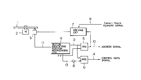
Fig. 4 is a block diagram of a drive to read the
address information in the sector identiying portion ID
and the control data CD from an optical disk 1 according
to the invention. The data recording and reproducing
section and the servo system are omitted in the diagram.
Reference numeral 1 denotes the optical disk; 2 is a
motor M; 3 an optical head to record or read out data onto
and from the optical disk 1; 4 a sector identifying
portion reproducing circuit to read out address information
of tracks and sectors from the sector identifying portion
ID; 5 and 6 AND circuits; 7 a seeking circuit for
performing seeking control to move the optical head 3 at a
high speed by a lineax motor and to seek a predetermined
-- 11 --
09178
1 track on the optical disk 1; and 8 an inverter.
In the diagram, the drive applies to the
seeking circuit 7 the address information of the control
track to be sought as a target track address signal 9.
The seeking circuit 7 compares an address signal 10 read
by the sector identifying portion reproducing circuit 4
with the target address signal ~ and accesses the optical
head 3 to an object track at a h.igh speed.
A reproduction signal 11 of the optical head 3 is
demodulated by the reproducing circuit 4 and a demodulation
signal 12 is output~ When the optical head 3 reads out
the sector identi~ying portion ID, the demodulation signal
12 indicates the track address in~ormation (track address
TA and sector address SA). On the other hand, when the
optical head 3 reads out the control field portion CF,
the demodulation signal 12 represents the control data CD.
The demodulation signal 12 is divided into an
address signal 10 and a control data signal 14 by the AND
circuits 5 and 6 on the basis of the.se_tor address data
SD and a fla~ F2 signal 13 as the most significant bit of
the control data byte B2. That is, when the identification
flag F2 signal 13 is set to "1", the AND circuit 5 is made
effective, sc that the address signal l0 is output. When
it is set to "0", the signal 13 is inverted by the inverter
8 and the AND circuit 6 is made effective, so that the
control data signal 14 is output.
If the clock of:the PE modulation or the like is
provided for each bit of.the sector identifying portion
- 12 -
1 309 1 78
1 ID, the sector identifying portion reproducing circuit
4 can directly regenerate clocks ~rom the reproduction
signal 11 without using the PLL circuit as mentioned above.
Even if the rotational speed of the disk changes in a
wide range, clocks can be preferably regenerated as
compared with the case of regenerating clocks by the
PLL circuit.
Therefore, the control track on the optical
disk of the invention can be easily read by various kinds
of driving apparatuses.
As will be obviously understood from the above
description, the control trac~s can be freely sought in
the same manner as the data track by setting the control
track so as to have the same sector format as that of
the data track. Further, by setting the control field
portion to the same format as that of the sector identifying
portion, the sector identifying portion reproducing circuit
can be commonly used to read the control data. In
addition, when using the modulating system such that
the modulation data bit has the clock bit, the address of
the control track can be accurately read by various kinds
of driving apparatuses and the control track can be
directly sought. Thus, the control data can be promptly
detected and the rise-up time of the drive when the disk
is exchanged can be fairly reduced. On the other hand,
since an enough reliability is derived even when using
the control tracks of the number within a range from a ~ew
tracks to a ten and a few tracks, the reduction of the
- I3 -
1 recording capacity is small.
As described above, accGrding to the invention,
a position seeking mechanism and a reading circuit of a
special control track are unnecessary and the control
data can be reproduced with a high reliability. Moreover,
the rise-up time of the drive upon exchange of the disk
can be remarkably reduced by directly seeking the control
track and the like. As mentioned above, practical
effects of the invention are large.
- 14 -