Note: Descriptions are shown in the official language in which they were submitted.
:~3~9~3~
SPECIFICATION
Title of the Invention
COIN SELECTOR
~ackqround of the Invention
1. Field of the Invention
The present invention relates to a coin selector in use
with various types of service machines such as a vending
machine and a coin exchanging machine, and more particularly
to a coin selector of the type in which different types of
coins are sorted by electronically recognizing the materials
or other properties of the coins.
2. Description of the Related Art
An example of the conventional coin selectors of the
type which electronically sorts coins is disclosed in US
Patent No. 3870137. The coin selector is so arranged that a
coil of an oscillator is disposed along one side of a coin
path. The coin selector electronically recognizes the type
of a coin in accordance with a deviation of an 05Ci llating
frequency of the oscillator, which deviation is caused when
the coin passes through the coin path. There are so-called
cladding coins, such as 10 cent, 25 cent and one dollar
coins. The cladding coin is formed by laminating thin
layers of different materials. I'he cladding coins cannot be
detected by using a single oscillator generating a signal of
a single frequency. As is well known, when a magnetic field
is applied to a coin, magnetic fluxes in a magnetic field
alternating at a low frequency penetrates deeply into the
coin, while magnetic fluxes in a magnetic field alternating
~131~3~
at a high frequency act only in the surface region of the
coin. Accordingly, a coin selector whose oscillator
oscillates at a frequency so selected as to detect the
material of the inner portion of a coin, cannot detect the
material of the surEace of the coin. To the contrary, a
coin selector whose oscillator oscillates at a frequency so
selected as to detect the material of the surface of a coin,
cannot detect the material of the inner portion of the coin.
To cope with this problem, the coin selector disclosed in
10 the US patent No. 3870137 uses a plurality of coils arrayed
along the coin path, and a plurality of oscillators in
connection with the coils. The oscillating frequencies of
the oscillators are made different from one another so as to
detect the cladding coins. This approach, however, creates
another problem that the array of the plurality of coils
along the coin path results in an elongation of the coin
path, and consequently an increase of a size of the coin
selector. The approach has a further problem that the
provision of the plurality of oscillators oscillating at
different frequencies requires an intricated circuit
arrangement.
In the coin selector of the US Patent No. 3870137, the
coin path i9 inclined by a predetermined angle with respect
to a vertical line. This is done ~o prevent a coin passing
through the coin path from moving in a direction transverse
to the path so as to maintain a fixed relationship of the
coils arrayed on one side of the coin path and the coin
~3~3~
passing through the coin path. If the coin path is arranged
exactly vertically, distance between a passing coin and the
coils changes as the coin moves transversely in the coin
path. As the distance between the coin and the coils
changes, the deviation of the oscillating frequency of the
oscillator changes. Therefore, the coin selec~or mistakenly
recognizes the types of the passing coin. However, the
inclined arrangement of the coin path creates another
problem. In the arrangement, a coin slides along one side
wall of the coin path. When the coin is wet, it tends to
jam in the pathO Further, in the arrangement, dusty
materials tend to deposit on the side wall of the path.
When dust is deposited to be a certain thick, a magnetic
coupling between a coin and each coil changes. Therefore, a
coin sliding down the dusty side wall provides an output
signal different from the output signal when the same coin
slides down on a clean side wall of the coin path. This
degrades an accuracy of the coin selection of the coin
selector, and possibly causes frequent improper operations
of the coin selector. Further, the inclined arrangement of
the coin path requires a larger space. This leads to an
increased size of the coin selector.
Summary of the Invention
Accordingly, an object of the present invention is to
provide a coin selector which is simple in construction and
is able to discriminately recognize the types of coins
stably and accurately.
According to one aspect of the present invention, there
~3~3~
is provided a coin selector comprising a first receiving
coil disposed along a coin path, a first exciting coil so
disposed as to magnetically couple with the first receiving
coil, a second receiving coil disposed facing the first
receiving coil with respect to the coin path, a second
. _
exciting coil so disposed as to magnetically couple with the
second receiving coil, drive means for exciting and driving
the first and second exciting coils, and judging means for
judging a coin passing through the coin path on the basis of
a signal representing the sum of the output signals of the
first and second receiving coils.
According to another aspect of the present invention,
there is provided a coin selector comprising a first
receiving coil disposed along a coin path, a first exciting
coil so disposed as to magnetically couple ~ith the first
receiving coil, a second receiving coil disposed facing the
first receiving coil with respect to the coin path, a second
exciting coil so disposed as to magnetically couple with the
second receiving coil, drive means for driving the first and
second exciting coils, coin diameter detecting means
disposed along the coin path for detecting a diameter of a
coin passing through the coin path, and judging means for
judging a coin by determining properties of a coin passing
through the coin path on the basis of a signal representing
the sum of the output signals of the first and second
receiving coils, and by determining a diameter of the coin
passing through the coin path on the basis of an output of
,,
!
~30~g3~
the diameter detecting means.
Tha first and second exciting coils are driven by the
drive means. A magnetic field developed by the Eirst
exciting coil acts on the first and second receiving coils.
A magnetic field devsloped by the second exciting coil ac~s
on the second and first receiving coils. When ~ coln is put
into and passes throuyh the coin path, the magnetic fields
of the first and second receiving coils and consequence the
output signals of those coils change. The recognizing means
10 recognizes properties a passing coin in accordance with a
signal representing the sum of the output signals of the
first and second receiving coils. The coin diameter
detecting means detects a diameter of the passing coin in
the coin path.
With such an arrangement, the coin selector is simple
in construction and reduced in size, and is able to exactly
recognize the properties of a passing coin in the coin path.
The arrangement of the coin selector allows the coin path to
be set vertically, not obliquely. The coin selector using a
20 vertically arrayed coin path is free from the problems of
the dusty material deposition and coin jamming in the coin
path, that are essential to the obliquely arrayed coin path
structure. Therefore, a stable and exact recognition of the
properties of coins may be realized.
Brief Description of the Drawinqs
Fig. 1 is a diagram showing a fundamental configuration
of a coin detecting section employed in the present
invention; J
130~3~
FigO 2 is a circuit diagrarn used in the configuration
of Fig. l;
Figs. 3 through 6 are diagrams u~eful in explaining the
operation of the Fig. 1 configuration;
Figs. 7 and 8 are graphical representations of the
output characteristics of the circuit of Fig. 2;
Fig. 9(a) shows a sectional view of an embodiment of a
coin selector according to the present invention as viewed
Erom the front;
10Fig. 9(b) shows a sectional view taken on line A - A of
Fig. 9(a);
Fig. lO~a) shows a front view showing an example of a
pot type coil used as a receiving coil;
Fig. lO(b) shows a sectional view taken on line ~ - B
in Fig. lO(a);
Fig. ll(a) shows a front view of an example of a drum
type coil used as an exciting coil;
Fig. ll(b) shows a sectional view taken on line C - C
in Fig ll(a);
20Fig. 12 is a partial sectional view showing how a coil
for recognizing the type of a coin is mounted;
Figs. 13 and 14 show sectional views showing
conEigurations oE other coils for recognizing tt-e type of a
coil;
Fig. 15 shows a circuit diagram of an example of a
circuit for recognizing the material and diameter of a coin;
Fig. 16 shows a waveform of an output signal of a
~3~3~
receiving coil when a coin is put into a coin path;
Fig. 17 shows a waveform of an output signal of an
integrating circuit when a coin is put into a coin path;
Fig. 18 shows a flowchart showing a processing to
recognize the material of a coin;
Fig. 19 is a circuit diagram of another e~bodiment of a
circuit for recognizing the material and diameter oE a coin;
Fig. 20 is a diagram showing an array of coils for
recognizing a coin diameter in the embodiment shown in Fig.
19; ancl
Fig. 21 is a sectional view showing another example of
a side wall of a coin path to which a coil for recognizing a
coin material is mounted.
Detailed _escription of the Preferred Embodiments
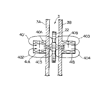
Fig. 1 is a sectional view of a park of a coin
detecting section employed in a coin selector according to
the present invention. In Fig. 1, a first receiving coil
40A is disposed on one side wall 3A of a coin path 3 through
which a coin 22 passes. A second receiving coil 40B is
disposed on the other side wall 3~ such that it is arranged
to be coaxial with the first receiving coil 40A. A first
exciting coil 41A is disposed adjacent to and coaxial with
the first receiving coil 40A. A second exciting coil 41B is
disposed adjacent to and coaxial with the second receiving
coil 40B.
Fig. 2 shows connections of the first and second
exciting coils 41A and 41B, and first and second receiving
coils 40A and 40B. The first and second exciting coils 41A ,
~3~9~3~
and 41B are connected in series to each other, and are
energized by a single drive source 23. The first and second
receiving coils 40A and 408 are also connected in series
with each other. 'rhe series circuit of the first and second
receiving coils 40A and 40~ is connected in parallel with a
capacitor 29. The type of a coin 22 put into the coin path
3 is recognized on the basis of an output voltage VOuT of
the series circuit of the first and second receiving coils
40A and 4OB.
The first and second exciting coils 41A and 41B are
energized by an AC signal alternately inverting its polarity
at predetermined periods that is derived from the drive
source 23. Accordingly, first and second states are
alternately set up in the first and second exciting coils
41A and 41~ in accordance with the alternately changing
polarities of the AC signal.
Fig. 3 shows a state of magnetic fluxes in the first
state, and Fig. 4 a state of magnetic fluxes in the second
state.
Referring to Fig. 3, in the first state before the coin
22 is put into the coin path 3, magnetic fluxes 401 and 402
developed by the exclting coil 41A pass through the
receiving coil 40A, to induce in the receiving coil 40A a
voltage corresponding to the magnetic fluxes 401 and 902.
Also in this state, magnetic fluxes 403 and 404 developed by
the exciting coil 41~ pass through the receiving coil 40~,
and magnetic flux 405, which is a part of magnetic flu~es
~3 3 ~
developed by the exciting coil 41A, passes through the
receiving coil 40s. As a result, a voltage is induced in
the receiving coil 40B by the magnetic fluxes 403, 404, and
405.
Referring to Fig. 4, in the second state before the
coin 22 is put into the coin path 3, magnetic f~uxes 401'
and 402' developed by the exciting coil 41A pass through the
receiving coil 40A, and magnetic flux 406 which is a part of
magnetic fluxes developed by the exciting coil 41B, passes
10 through the recPiving coil 40A. As a result, a voltage is
induced in the receiving coil 40~ by the magnetic fluxes
403, 404, and 405 .
Also in this state, magnetic fluxes 403' and 404'
developed by the exciting coil 41B pass through the
receiving coil 40B, to induce in the receiving coil 40B a
voltage corresponding to the magnetic fluxes 403' and 404'.
In Figs. 3 and 4, it is assumed now that under these
conditions, the coin 22 is put into the roin path 3. The
magnetic fluxes 401, 402, 401' and 402' that are developed
20 by the exciting coil 41A, when they reach the coin 22, are
influenced by an eddy current generated in the surface part
of the coin 22, and hence change. The change of the
magnetic fluxes causes the induced voltage in the receiving
coil 40A to change. In the same manner, the magnetic eluxes
403, 404, 403', and 404' that are developed by the exciting
coils 41B, when they read the coin 22, are influenced by an
eddy current generated in a surface part of the coin 22, and
change. The change of the rnagnetic fluxes causes the
-~ 3~3~
reduced voltage in the receiving coil 40B to change. On the
other hand, the magnetic fluxe~ 405 and 406 penetrate into
and passes through the coin 22. During the passage of the
fluxes, the fluxes 405 and 406 are influenced by the
material of the coin 22 in its central part, so as to change
the induced voltages in the receiving coils 40B and 40A,
respectively change. In this way, the voltage VOuT, which
is the sum of the output voltages of the receiving coils 40A
and 40B, changes in accordance with the materials of the
coin 22 in the surface and central parts. In other words,
the voltage VOuT contains the information regarding the
different materials of the coin in the surface and central
portions.
The output voltages of the receiving coils 40A and 40B
also change in accordance with a distance between the coils
and the coin 22 as the coin 22 passes through the coin path.
When the coin 22 ~races a path at the center of the coin
path so that it maintains the equal distance from the
receiving coils 40A and 40B, the voltages induced in the
receiving coils 40A and 40B are equal to each other.
However, when the coin traces a path deviated toward the
receiving coil 40A from the center of the coin path as shown
in Fig. 5, the influence by the coin 22 on the receiving
coil 40A increases and an output signal of the receiving
coil 40A increases. On the other hand, the influence by the
coin 22 on the receiving coil 40B decreases and an output
signal of the coil 40B decreases. Similarly, when the coin
~30~3~
traces a path deviated toward the receiving coil 40B from
the center oE the coin path as shown in Fig. 6, the
influsnce by the coin 22 on the receiving coil 40B increases
and an output signal of the coil 40B increases. On the
other hand, the influence by the coin 22 on the coil 40A
decreases and an output signal of the coil 40A decreases.
Whatever paths the coin may trace, the summation of the
induced voltages of the receiving coils 40A and 40B is
always constant.
With the connection of the receiving coils 40A and 40s
as shown in Fig. 2, the induced voltages of the receiving
coils 40A and 40B are summed to cancel the influences du~ to
the transverse displacement of the path traced by the coin
22 in the coin path 3.
Fig. 7 is a graph showing a variation of the output
voltage VOuT of the circuit of Fig. 2 when the coin 22
passes through the coils, with the abscissa representing a
frequency of the exciting voltage and the ordinate
representing the output voltage VOuT. In Fig. 7, if the
exciting frequency is set at "fo", the output voltage VOuT
shows Vo before the coin 22 is put into the coin path.
Under this condition, the output voltage VO~T exhibits a
peak voltage Vo at the frequency "fo". When the coin 22 is
put into the coin path 3, inductances of the receiving coils
40A and 40B change and the frequency at which the output
voltage VOuT exhibits a peak value, changes. Assuming that
the inductances of the receiving coils 40A and 40B before
the coin 22 is put into the path are Ll and L2, and that a
11
`
' . ' ! '
capacitance of the capacitor 29 is C, the ~esultant
inductance of th~ coils 40A and 40B is L = Ll ~ L2, and the
output voltage VOUT exhibits a maximum value at frequency
"fo" (= 1/2 ~). When the coin 22 is put into the coin
path 3, the resultant inductance L changes to an inductance
~', and a frequency at which the output voltage VOU~
exhibits a maximum voltage change to fl = 1/2 ~ . The
frequency difference f is 1/2 ~ 1/2 ~LV~
The peak value of the output voltage VOUT changes from
Vo to Vl as the coin 22 passes through the coils. At the
frequency of fo, the output voltage VOUT changes from Vo to
V2 due to the ccin 22 passing through the coils. A voltage
difference ~V (= V0 - V2) depends on the materials of the
coin 22. Ther~fore, the voltage difference AV is employed
to discriminate the types of coins in this embodiment.
Figs. 9(a) and 9tb) show an overall configuration of an
embodiment of a coin selector according to the present
invention in which Fig. 9(a) shows a sectional view of the
coin selector as viewed from the front side of the selector,
and Fig. 9(b) shows a sectional view taken on line A - A in
Fig. 9(a). In Figs. 9(a) and 9tb), like reference symbols
are used for designatlng like or equivalent portions in the
basic configuration shown in Fig 1.
In these drawings, a slot 2 is provided at the top of a
main frame of the coin selector 1. The coin 22 as put into
the slot 2 drops on a first rail 3R slanted down in the
direction going away from the slot 2. The coin 22 drops and
~L3~3~
rolls down on the rail 3R. A coil 4 for detecting the
materials and construction of the coin and a coil 5 for
detecting the size oE it are disposed around the middle of
the rail 3R. A processing to discriminately select coins
passing through the coin path is conducted based on the
outputs of the coils 4 and 5, which will be described
later.
A solenoid 6 is energized in response to truth or false
of the coin 22 as put in, under control of the coin select
processing previously conducted. When it is energized, a
gate 7 is driven to allow the coin to go to a true coin path
8, if the coin is true. If the coin is false, the coin is
directed to a false coin path 9. More specifically, in the
case of the false coin, the solenoid 6 is not energized and
the gate 7 lies in the true coin path 8. Accordingly, the
coin is directed into the false coin path 9. When the coin
is true, the solenoid 6 is energized to retract the gate 7
from the true coin path 8 in which the gate 7 is placed in a
stand-by state, to allow the true coin to go into the true
coin path 8.
The coins led to the path 8 are sorted into groups of
coins A and ~, and C and D in accordance with the
denominations of coins. When the coin belongs to the group
the coin of the denomination A or B, the solenoid 11 is
driven and the lever 13 is rotated clockwise in Fig. 9(a),
and the path leading to the group the coin of the
denomination C or D is closedr and the coins of the
denomination A or B are led to the rail 10. When the coins
13~3~ :
are of the denomination C or D, the solenoid 11 is not
driven and the coins pass under th~ coin path 8.
The coin of the denomination A or B led to the rail 10
is directed to either of paths 12A and 12B in accordance
with the si~e of the coin. The coin of the denomination C
or D passed through the true coin path 8 is directed to
either of paths 12C and 12D in accordance with the size of
the coin. The coin led to the false path 9 is discharged
through an exit (not shown)O
The coil 4 for recognizing properties of a coin, such
as material, size and surface condi-tions of the coin, has
substantially the same basic configuration as that of Fig.
1, and is composed of the receiving coils 40A and 40B, and
the exciting coils 41A and 41B.
The receiving coils 40A and 40B, as shown in Fig. lOta)
showing its front view and Fig. lO~b) showing a sectional
view taken on line B - B Fig lO(a), are each made up of a
pot type coil arranged such that a coil 40 wound around a
bobbin 43 is disposed in a pot type core 42 having a
cylindrical bore 42a at the center.
The exciting coils 41A and 41B, as shown in Fig. ll(a)
showing its front view and in Fig. ll~b) showing a sectional
view taken on line C - C in Fig. ll(a), are each made of a
drum type coil arranged such that a coil 41 i5 wound around
a drum type core 44 with a projection 94a at the center,
that will be fitted into the bore 42a of the pot type core
42. The core 92 for the pot type coil and the core 94 for
1~
~3~9~35
the drum type coil may be made of magnetic material such as
ferrite. The bobbin 43 for the pot type coil may be made of
nonmagnetic material such as plastic.
The receiving coils 40A and 40B and the exciting coils
41A and 41s, that are structured as shown above, are
arranged as shown in Fig. 12. The projection 4~a located at
the central part of the exciting coil 41A is fitted into the
bore 42a of the receiving coil 40A. Under this condition,
the surface of the receiving coil 40a that is opposlte to
10 the mounting surface of the exciting coil 41A is tightly
mounted on the side wall 3A of the coin path 3. In the same
manner, the exciting coil 41B is fitted to the receiving
coil 40B, and then is mounted on the side wall 3B of the
coin path 3 such that the axis of the exciting coil 41B and
the receiving coil 40B is aligned with that of the exciting
coil 41A and the receiving coil 40A mounted on the side wall
3A.
In the above instancet the receiving coils and the
exciting coils are separately formed. However, those may be
20 assembled into a single core as shown in Figs. 13 and 14.
Fig. 13 Rhows a coil arrangement in which coils 40 and 41
respectively wound on bobbins 45 and 46 are disposed in an
integrally formed core 44. In Fig. 13, a couple of coil
assemblies of the receiving and exciting coils thus arranged
are disposed on both sides of the coin path, with the coil
40 of each coil assembly facing the coin path. In a coil
assembly shown in Fig. 14, a bobbin 48 wound by coils 40 and
41 is assembled into a unit core 47. A couple of the coil
3 ~
assemblies are disposed on both sides o~ a coin path through
which a coin passes, with the coil gO of each assembly
facing the coin path.
The coil 5 for detecting the diameter of coins is made
up of an exciting coil mounted on one side wall of the first
rail 3R and a receiving coil mounted on the other side wall,
as will subsequently be described. The diameter of the coin
is recognized on the basis of a level change of an output
voltage of the receiving coil. The mounting position of the
coil 5 is deviated Erom the first rail 3R by a predetermined
distance in order to make it easy to recognize the coin
diameter.
Description to follow is an elaboration of a circuit
arrangement to determine the type of the coin 22 by using
the receiving coils 40A and 40B and the exciting coils 41A
and 41B.
Fig. 15 shows an embodiment of a circuit for
determining the properties of a coin put into a coin path,
such as material, size and surface conditions of the coin.
The first receiving coil 40A, first exciting coil 41A,
second receiving coil 40B, and second excitinq coil 41B make
up a property coil 4 for detecting the properties of a coin.
The exciting coils 41A and 41B for exciting the property
detecting coil 4 and the exciting coil 5A for exciting the
diameter-detecting coil 5 are connected in series, and then
connected to the output of a drive circuit 23. The drive
circuit 23 receives an AC exciting signal of 20 to 60 kHz,
16
3 ~
Eor example, that is derived from ~ freguency divider 24.
The frequency divider 24 frequency divides a pulse signal of
a reference frequency outputted from a central processing
unit (CPU) 25 into the siynal at 20 to 60 kHz. The dlive
circuit 23 amplifies the AC exciting signal and supplies it
to the exciting coils 41A, 41B and 5A. The ~C exciting
signal may be a signal of a sinusoidal wave or a signal of a
nonsinusoidal wave such as a rectangular wave, triangle wave
and a saw-tooth signal.
The receiving coils 40A and 40B of the property-
detecting coil 4 are connected in series and then connected
in parallel to a capacitor 29 for parallel resonance. The
capacitor 29, which is inserted in the series circuit of the
coils 40A and 40B, is connected across the input of an
amplifier/detector circuit 30A.
The receiving coil 5B for the diameter detecting coil 5
i8 coupled in parallel with a capacitor 28 for parallel
resonance which is further coupled across the input of an
amplifier~detector circuit 30B.
The amplifier/detector 30A amplifies and detects a high
frequency signal induced in the series circuit made up of
the receiving coils 40A and 40B, and outputs an envelope of
the high frequency signal.
Fig. 16 shows an example of a waveform of a high
frequency induced in the series circuit of the receiving
coils 40A and 40B. The high frequency signal indicates a
state of the coin 22 that is passing through the coin path
3. The amplifier/detector circuit 30A amplifies and detects
. .
3~3~
the high frequency signal 34 and extracts a variation in an
envelope 35 o the high frequency signal 34. The output
signal of the circuit 30A is inputted into an integration
circuit 31A.
The integration circuit 31A integrates the detected
signal of the amplifier/detector circuit 30A, to form a
voltage signal corresponding to the detected signal. An
example of the voltage signal outputted from the integration
circuit 31A is illustrated in Fig. 1~. The voltage signal
shown in Fig. 17 corresponds to the high frequency signal
shown in Fig. 0. A voltage VA in Fig. 17 shows a voltage
drop due to the passage of the coin 22. The output signal
of the integration circuit 31A is converted into a
corresponding digital signal by an A/D converter 26 and is
applied to the CPU 25.
Similarly, an output signal of the receiving coil 5B is
amplified and detected by the amplifier/detector circuit
30B, and is integrated by the integration circuit 31B, and
converted into a corresponding digital voltage signal by the
A/D converter 26, and finally inputted into the CPU 25.
The CPU 25 decides the properties of the coin 22 on the
basis of an amount of the drop of each of the induced
voltages in the receivlng coils 40A and 40B that is caused
by the passage of the coin 22. The CPU 25 also decides the
diameter of the coin 22 on the basis of an amount of the
drop of the induced voltage in the receiving coil 5B. The
programs for the decision of the properties and the diameter
18
!3 3 ~
of the coin and the data ~oncernlng a level to discriminate
the amounts of the voltage drop are stored in a read only
memory (ROM) 33.
After decided the properties and the diameter of the
coin, the CPU 25 decides if the passing coin 22 is true or
false. If it is true, the CPU 25 drives a true/false
selecting solenoid 6 through a solenoid driver 32A.
Further, the CPU 25 decides the type of denominations A, B,
C or D of the coin 22. If the coin 22 belongs to the
denominations A or B, the CPU 25 drives a denomination
selecting solenoid 11 by a solenoid drive circuit 32B,
Interface terminals 25A to 25D of the CPU 25 are for
driving devices such as a display.
Fig. 18 shows a flowchart showing a processing flow to
recognize passing coins that is executed by the CPU 25.
The operation of the circuit of Fig. 15 will be
described with reference to the above flowchart.
When a power supply is turned on, the CPU 25
initiali~es internal register~ and the like, and fetches
various types of data for coin recognition from the ROM 33
(steps 46 and 47). After this, the CPU 25 makes an error
check as to whether or not an erroneous drive signal is
applied to the denomination solenoid ll and the like. For
the error check, the output signal of the A/D converter 26
ln a stand-by mode is measured as a reference voltage signal
tsteps 48 and 49). The measurement of the voltage signal of
the A/D converter 26 in the stand-by mode is made to detect
an amount of the output voltage drop of the A/D converter 26
19
1 3 1~
that results from the inserting of a coin, in the form of a
value relative to the value of the reference voltage signal
in the stand-by mode. That mea~urement ensures an exact
detection of an amount of the output voltage drop of the A/D
converter 26 that is caused by the passage of the coin,
regardless of a variation of the power source voltage and an
aging of the exciting coils 41A and 41B.
After the output voltage (reference voltage) of the A/D
converter 26 in the stand-by mode is loaded into the
internal register RO, the CPU 25 waits for another coin to
be inputted ~steps 50 and 51).
When the coin 22 is inputted from the slot 2, the~CPU
25 starts to collect the coin data ~step 52). The exciting
coils 41A and 41B, and 5A are excited by an exciting signal
outputted from the drive circuit 23. As a result,
predetermined voltages are induced in the receiving coil~
40A, 40B and 5B through magnetic couplings with the
corresponding exciting coils. A coin 22 is put into the
coin path, and passeR the locations of those receiving coils
20 40A, 40B and SB. The passage o~ the coin 22 changes the
magnetic fluxes acting the receiving coils 40A, 40B and 5B
which are magnetically coupled with the receiving coils 40A,
40B and 5B, and consequently changes the induced voltage in
the receiving coils 40A, 40B and 5B. The amounts of these
voltage changes depend on the propertieq and diameter of the
passing coln. If the passing coin is true, the voltage
change is determined by value~ proper to the true coin of
13~3~
each denomination.
The output voltages of the receiving coils 40A, 40B and
5B are respectively amplified and detected by the
amplifier/detector circuits 30A and 30B and integrated by
the integration circuits 31A and 31~. As a result, the
integration circuits 81A and 31B produce respectively
voltage signals each varying as shown in Fig 17 in
accordance with the denomination of the coin 22. The CPU 25
fetches the variations of the output signals of the
integration circuits 31A and 31B that results from the coin
passage, in the for~ of coin data7 An amount of the voltage
change Vx (X represents the denominations of coins A to D)
of each of the output signals of the integration circuits
31A and 31B is compared with reference values RVX
representing the amount o~ voltage change for each
denomination of coins that are stored in and read out from
the ROM 33, to find the denomination of the coin (steps 53
and 54).
If it turns out that the coin does not belong to any
denomination and therefore the coin i~ a false coin, the
solenoid 6 is not energized and the coin i5 discharged
through a discharging slot. If it turns out that the coin
belongs to one of the denominations A to D, the solenoid 6
is driven to lead the coin 22 to the true coin path 8.
Then, if the coin belong~ to the denominations of coins A or
B, the solenoid 11 is driven to lead the coin to the path
12A or 12~. If the coin belongs to the denomination C or D,
the solenoid 11 is not driven, and the coin is led to the
~3~3~
path 12C or 12D tstep 55).
The combination of the exciting coil 41A and receiving
coil 40A and the combination of the exciting coil 41B and
the receiving coil 40B are oppositely disposed with respect
to the side walls 3A and 3B o~ the coin path (first rail
3R). Accordingly, even if the coin 22 passes ~hrough the
coin path along a path set aside to either of the side walls
3A and 3B, the sum of the induced voltages in the receiving
coils 40A and 40B is always constant for the same
denomination of passing coins.
Let us consider a case, for example, that the coin 22
passes along a path closer to the sida wall 3A in the coin
path and that an amount of the induced voltage drop in the
receiving coil 40A is increased and becomes larger than that
caused when the coin 22 passes along a path extending at the
center of the coin path. In this case, an amount of the
induced voltage drop in the receiving coil 40B is decreased
by a value corresponding to the increase in the receiving
coil 40A. Therefore, the sum of the induced voltages in the
20 receiving coils 40A and 40B i5 constant. Thus, correct
voltage is detected regardless of the path the coin 22 takes
in the coin path.
With the arrangement of the coin selector as mentioned
above, if in place of a cladding coin in which a core layer
of copper is laminated with a cupro-nickel layer, such as
coins of 10 and 25 cent, and one dollar that are currently
used in U.S.A., a coin of copper whose outer configuration
3 5
and the thickness are the same as those of the cladding coin
is inputted, the coin selector according to the present
invention may readily recognize the copper coin. Thus,
according to the embodiment, difference between the cladding
coin and the copper coil is distinctly observed. Therefore,
the coin selector may correctly sort the cladding coin and
the copper coin.
The arrangement of the coin selector eliminates a
necessity for slanting the coin path to slide coins on
either of the side walls of the coin path. Accordingly, the
coin path for detecting the coin may be arrayed vertically.
Therefore, no dusty materials are deposited on the coin
path. Further, a passing coin, even if it is wet, will
smoothly travel in the coin path. Fig. 21 shows the
irregular ~urfaces of the side walls 3A and 3B of the coin
path on which the coil 4 is disposed for preventing a we-t
coin from ~ticking to the side wall surfaces.
Further, according to the embodiment, only two groups
of coils, the property detecting coil 4 and the diameter
detecting coil 5, are disposed at the first rail 3R.
Therefore, the rail may be substantially shortened.
In the above-mentioned embodiment, the exciting coils
41A and 41B for the property detecting coil 4 and the
exciting coil 5A for the diameter detecting coil 5 are
connected in series, and are energized by the single drive
circuit 23. Accordingly, a frequency of an exciting signal
applied to the exciting coils 41A and 41B is equal to that
of an exciting signal applied to the exciting coil 5A of the
23
:: ~
13~3~
diameter detecting coil 5.
Alternatively, the exciting coils 41A and 41B for the
property detecting coil 4, and the exciting coil 5A of the
diameter detecting coil 5 may be arranged in parallel and
couplea with the drive circuit 23. Those coils may be
energized by different drive circuits, respectively.
Further, although the exciting coils 41A and 41~ are
connected in series and energized by one drive circuit 23,
if required, these exciting coils may be connected in
10 parallel to the drive circuit 23. Further, these coils may
be driven by two independent drive circuits.
The receiving coils 40A and 40s, that are connected in
series in the above mentioned embodiment, may be connected
in any manner so long as the voltages induced in those coils
are summed and applied to the amplifier/detector circuit
30A.
Although the pairs of the exciting and receiving coils
40A and 41A, 40B and 41B are aligned and face with each
other, these pairs of the coi 18 may be disposed out of the
20 alignment so long a~ the paired colls satisfy a
predetermined magnetic coupling relationship. Further,
relative position of the exciting coil and the receiving
coil in each pair may be changed so long as they are
magnetically coupled with each other with a magnetic
coupling strength greater than a predetermined level.
The same thing is true for the alignment of each coil
in the paired coils.
~t
24
9 ~ ~ ~
Fig. 19 is a block diagram showing a modiication of
the coin selector. In the modification, two coils 5 and 5'
are used for the coil for detecting the diameter of a coin.
Structurally, as shown in Fig. 20, the first coil 5 is
disposed at a location suitable for detecting a large coin
22L having the maximum diameter. The second coil 5' is
located at the best place to detect a small coin 22S of the
minimum diameter. With the use of the two coils for the
diameter detecting purpose, the diameters of the coils may
10 be reduced. The diameter reduction reduces a space required
for disposing the property detecting coils and the diameter
detecting coils~ As a result, the size of the coin selector
may be further reduced.